

Datasheet SST45VF512-10-4C-SA, SST45VF020-10-4C-SA, SST45VF010-10-4C-SA Datasheet (Silicon Storage Technology)
Page 1

512 Kbit / 1 Mbit / 2 Mbit Serial Flash
SST45VF512 / SST45VF010 / SST45VF020
FEATURES:
• Single 2.7-3.6V Read and Write Operations
• Serial Interface Architecture
– SPI Compatible: Mode 0 and Mode 3
• Byte Serial Read with Single Command
• Superior Reliability
– Endurance: 100,000 Cycles (typical)
– Greater than 100 years Data Retention
• Low Power Consumption:
– Active Current: 20 mA (typical)
– Standby Current: 10 µA (typical)
• Sector or Chip-Erase Capability
– Uniform 4 KByte sectors
• Fast Erase and Byte-Program:
– Chip-Erase Time: 70 ms (typical)
– Sector-Erase Time: 18 ms (typical)
– Byte-Program Time: 14 µs (typical)
Advance Information
• Automatic Write Timing
– Internal VPP Generation
• End-of-Write Detection
– Software Status
• 10 MHz Max Clock Frequency
• Hardware Reset Pin (RESET#)
– Resets the device to Standby Mode
• CMOS I/O Compatibility
• Hardware Data Protection
– Protects and unprotects the device
from Write operation
• Packages Available
– 8-Pin SOIC (4.9mm x 6mm)
1
2
3
4
5
6
7
PRODUCT DESCRIPTION
The SST45VF512, SST45VF010 and SST45VF020 are
manufactured with SST’s proprietary, high performance
CMOS SuperFlash technology. The Serial Flash is
organized as 16 sectors of 4096 Bytes for SST45VF512,
32 sectors of 4096 Bytes for the SST45VF010 and
64 sectors of 4096 Bytes for the SST45VF020. The
memory is accessed for Read or Erase/Program by the
SPI bus compatible serial protocol. The bus signals are:
serial data input (SI), serial data output (SO), serial clock
(SCK), write protect (WP#), chip enable (CE#), and
hardware reset (RESET#).
The SST45VFxxx devices are offered in 8-pin SOIC
package. See Figure 1 for the pinout.
Device Operation
The SST45VFxxx uses bus cycles of 8 bits each for
commands, data, and addresses to execute operations.
The operation instructions are listed in Table 2.
All instructions are synchronized off a high to low transition of CE#. The first low to high transition on SCK will
initiate the instruction sequence. Inputs will be accepted
on the rising edge of SCK starting with the most significant bit. Any low to high transition on CE# before the input
instruction completes will terminate any instruction in
progress and return the device to the standby mode.
Read
The Read operation outputs the data in order from the
initial accessed address. While SCK is input, the address
will be incremented automatically until end (top) of the
address space, then the internal address pointer automatically increments to beginning (bottom) of the address space (00000H), and data out stream will continue.
The read data stream is continuous through all addresses until terminated by a low to high transition on
CE#.
Sector/Chip-Erase Operation
The Sector-Erase operation clears all bits in the selected
sector to “FF”. The Chip-Erase instruction clears all bits
in the device to “FF”.
Byte-Program Operation
The Byte-Program operation programs the bits in the
selected byte to the desired data. The selected byte must
be in the erased state (“FF”) when initiating a Program
operation. The data is input from bit 7 to bit 0 in order.
Software Status Operation
The Status operation determines if an Erase or Program
operation is in progress. If bit 0 is at a “0” an Erase or
Program operation is in progress, the device is busy. If bit
0 is at a “1” the device is ready for any valid operation. The
status read is continuous with ongoing clock cycles until
terminated by a low to high transition on CE#.
8
9
10
11
12
13
14
15
16
© 2000 Silicon Storage Technology, Inc. The SST logo and SuperFlash are registered trademarks of Silicon Storage Technology, Inc. These specifications are subject to change without notice.
514-1 10/00 S71178
1
Page 2
512 Kbit / 1 Mbit / 2 Mbit Serial Flash
SST45VF512 / SST45VF010 / SST45VF020
Advance Information
Reset
Reset will terminate any operation, e.g., Read, Erase
and Program, in progress. It is activated by a high to low
transition on the RESET# pin. The device will remain in
reset condition as long as RESET# is low. Minimum reset
time is 10µs. See Figure 14 for reset timing diagram.
RESET# is internally pulled-up and could remain unconnected during normal operation. After reset, the device is
in standby mode, a high to low transition on CE# is
required to start the next operation.
An internal power-on reset circuit protects against accidental data writes. Applying a logic level low to RESET#
during the power-on process then changing to a logic
level high when V
level will provide additional protection against accidental
writes during power on.
Read SST ID/Read Device ID
The Read SST ID and Read Device ID operations read
the JEDEC assigned manufacturer identification and the
manufacturer assigned device identification codes.
These codes may be used to determine the actual device
resident in the system.
has reached the correct voltage
DD
TABLE 1: PRODUCT IDENTIFICATION
Byte Data
Manufacturer’s ID 0000 H BF H
Device ID
SST45VF512 0001 H 41 H
SST45VF010 0001 H 45 H
SST45VF020 0001 H 43 H
514 PGM T1.4
Write Protect
The WP# pin provides inadvertent write protection. The
WP# pin must be held high for any Erase or Program
operation. The WP# pin is “don’t care” for all other
operations. In typical use, the WP# pin is connected to
VSS with a standard pull-down resistor. WP# is then
driven high whenever an Erase or Program operation is
required. If the WP# pin is tied to VDD with a pull-up
resistor, then all operations may occur and the write
protection feature is disabled. The WP# pin has an
internal pull-up and could remain unconnected when not
used.
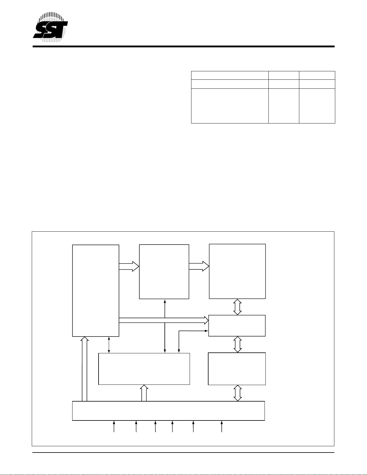
FUNCTIONAL BLOCK DIAGRAM
Address
Buffers
and
Latches
X - Decoder
Control Logic
Serial Interface
SuperFlash
Cell Array
Y - Decoder
I/O Buffers
and
Data Latches
© 2000 Silicon Storage Technology, Inc.
CE#
SCK SI SO WP# RESET#
2
514ILL B1.0
S71178
514-1 10/00
Page 3
512 Kbit / 1 Mbit / 2 Mbit Serial Flash
SST45VF512 / SST45VF010 / SST45VF020
Advance Information
WP#
V
DD
CE#
SCK
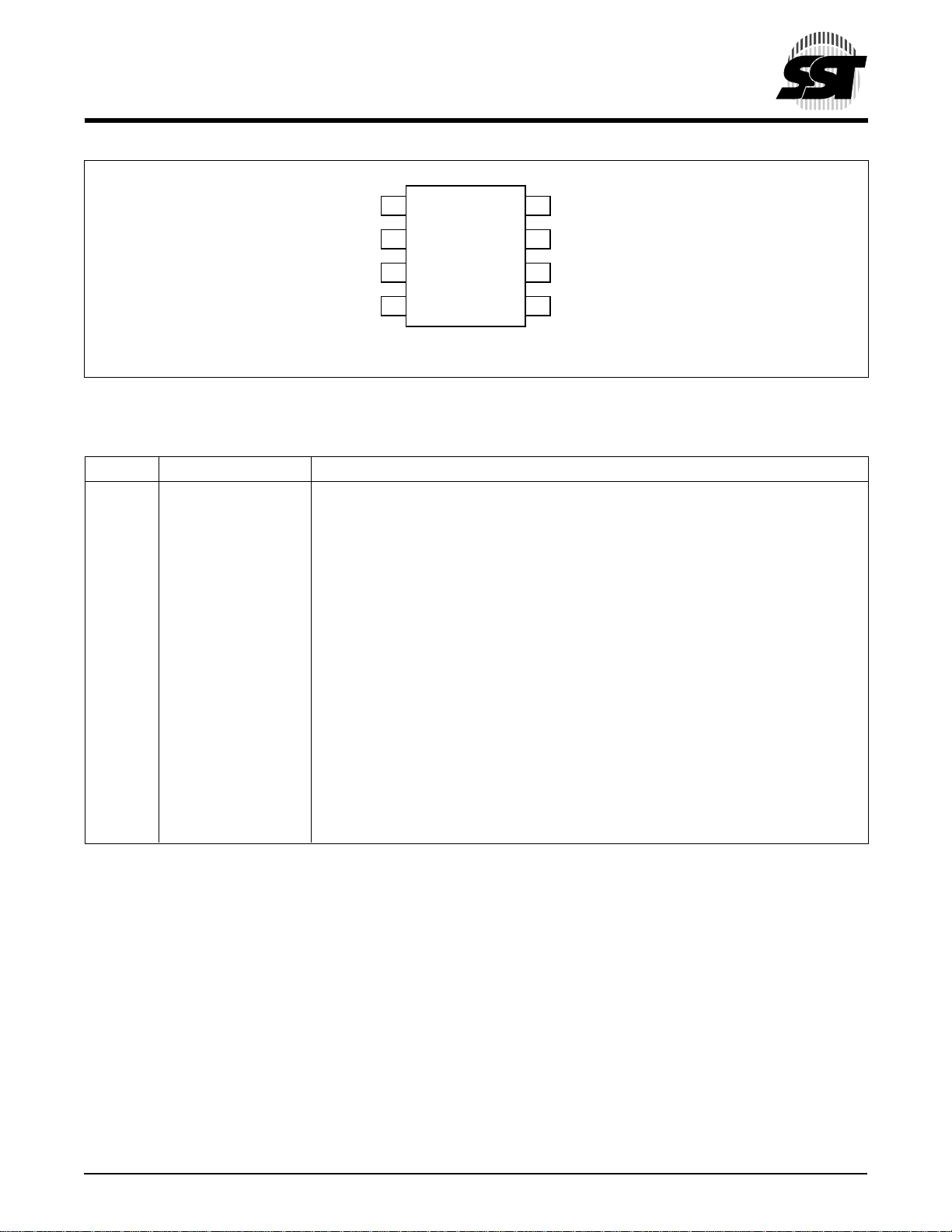
FIGURE 1: PIN ASSIGNMENTS FOR 8-PIN SOIC
TABLE 2: PIN DESCRIPTION
Symbol Pin Name Functions
SCK Serial Clock To provide the timing of the serial interface. Commands, addresses, or
input data are latched on the rising edge of the clock input, while output
data is shifted out on the falling edge of the clock input.
SI Serial Data Input To transfer commands, addresses, or data serially into the device. Inputs
are latched on the rising edge of the serial clock.
SO Serial Data Output To transfer data serially out of the device. Data is shifted out on the
falling edge of the serial clock.
CE# Chip Enable The device is enabled by a high to low transition on CE#.
WP# Write Protect To protect the device from unintentional Write (Erase or Program)
operations. When WP# is low, all Erase and Program commands are
ignored. When WP# is high, the device may be erased or programmed.
This pin has an internal pull-up and could remain unconnected when not used.
RESET# Reset A high to low transition on RESET# will terminate any operation in progress
and reset the internal logic to the standby mode. The device will remain in the
reset condition as long as the RESET# is low. Operations may only occur
when RESET# is high. This pin has an internal pull-up and could remain
unconnected when not used.
V
DD
V
SS
Power Supply To provide power supply (2.7-3.6V).
Ground
1
2
Standard Pinout
T op Vie w
3
Die Up
4
8
7
6
5
514 ILL F01.0
RESET#
V
SS
SO
SI
514 PGM T2.2
1
2
3
4
5
6
7
8
9
10
11
12
© 2000 Silicon Storage Technology, Inc.
13
14
15
16
3
S71178
514-1 10/00
Page 4
512 Kbit / 1 Mbit / 2 Mbit Serial Flash
SST45VF512 / SST45VF010 / SST45VF020
Advance Information
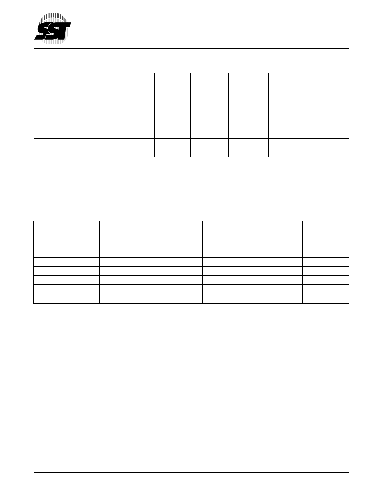
TABLE 3: DEVICE OPERATION INSTRUCTIONS
Bus Cycle 1 2 3 4 5 6 7 and after
1
Operation/Type Command Address
Read FFH A
Sector-Erase
2
20H A23-A
23-A16
16
Chip-Erase 60H X X X D0H X
Byte-Program 10H A23-A
16
Software-Status 9FH Dout
Read SST ID 90H X X A
Read Device ID
Notes:
1. A23-A16 are “Don't Care” for SST45VF512, A23-A17 are “Don't Care” for SST45VF010, A23-A18 are “Don't Care” for SST45VF020.
2. A16-A12 are used to determine sector address, A11-A8 are don't care.
3. With A15-A1 = 0, SST45VF512 Device ID = 41H, is read with A0 = 1.
With A16-A1 = 0, SST45VF010 Device ID = 45H, is read with A0 = 1.
With A17-A1 = 0, SST45VF020 Device ID = 43H, is read with A0 = 1.
3
90H X X A0=1 Device ID
Address Address Data Dummy Data
A15-A
A15-A
A15-A
8
8
8
A7-A
0
X X Dout
X D0H X
A7-A
0
=0 BFH
0
Din X
514 PGM T3.3
TABLE 4: DEVICE OPERATION TABLE
Operation SI SO CE#
1
WP# RESET#
Read X Dout Low X High
Sector-Erase X X Low High High
Chip-Erase X X Low High High
Byte-Program Din X Low High High
Software-Status X Dout Low X High
2
Reset
X XXXLow
Read SST ID X Dout Low X High
Read Device ID X Dout Low X High
Notes:
1. A high to low transition on CE# will be required to start any device operation except for Reset.
2. The RESET# low will return the device to standby and terminate any Erase or Program operation in progress.
514 PGM T4.1
© 2000 Silicon Storage Technology, Inc.
4
S71178
514-1 10/00
Page 5
512 Kbit / 1 Mbit / 2 Mbit Serial Flash
SST45VF512 / SST45VF010 / SST45VF020
Advance Information
Absolute Maximum Stress Ratings (Applied conditions greater than those listed under “Absolute maximum Stress
Ratings” may cause permanent damage to the device. This is a stress rating only and functional operation of the device
at these conditions or conditions greater than those defined in the operational sections of this data sheet is not implied.
Exposure to absolute maximum stress rating conditions may affect device reliability.)
1
Temperature Under Bias ................................................................................................................. -55°C to +125°C
Storage Temperature ...................................................................................................................... -65°C to +150°C
D. C. Voltage on Any Pin to Ground Potential ............................................................................ -0.5V to V
Transient Voltage (<20 ns) on Any Pin to Ground Potential........................................................ -1.0V to V
DD
+ 1.0V
DD
+ 0.5V
Package Power Dissipation Capability (Ta = 25°C) ........................................................................................... 1.0W
Surface Mount Lead Soldering Temperature (3 Seconds)............................................................................... 240°C
Output Short Circuit Current
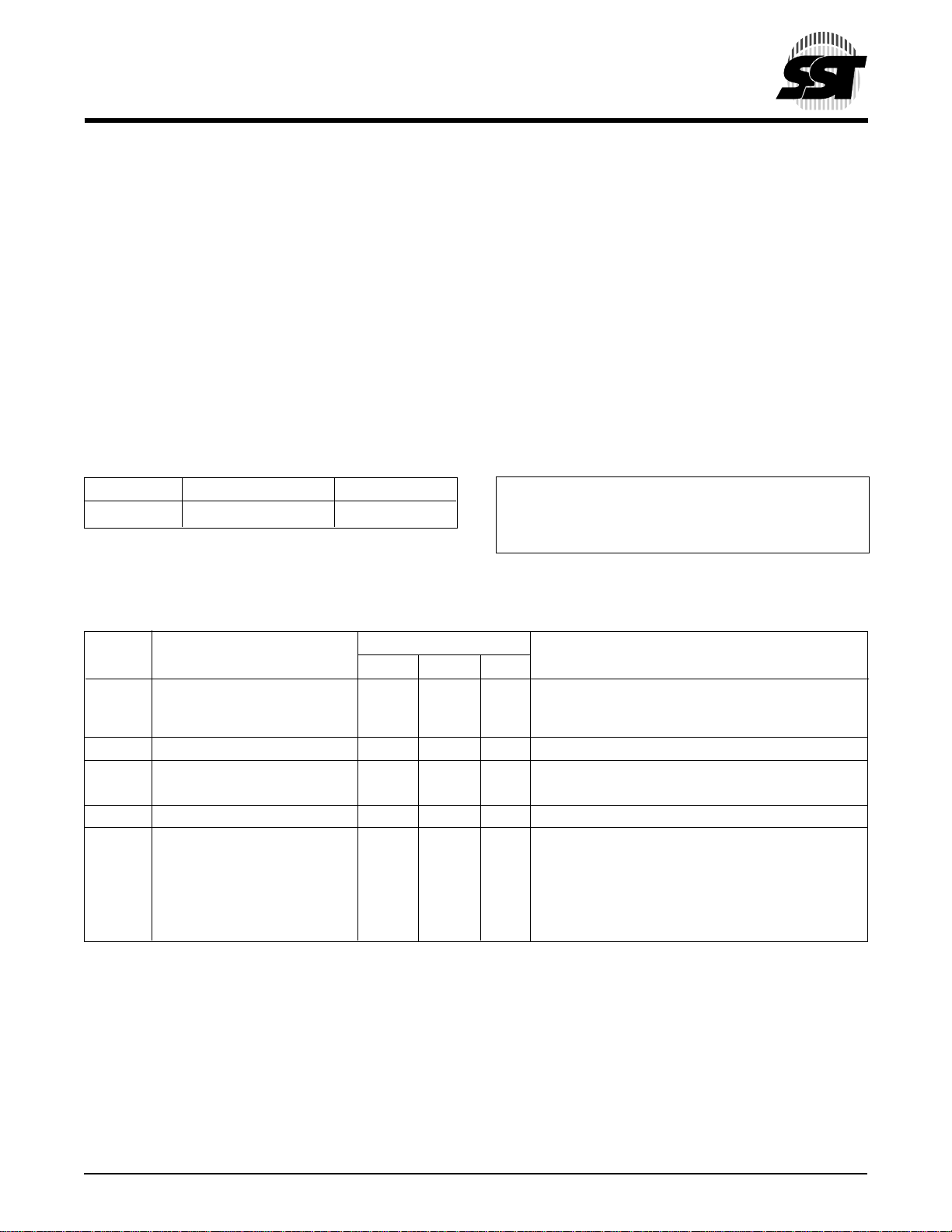
OPERATING RANGE
Range Ambient Temp V
Commercial 0 °C to +70 °C 2.7-3.6V
1
................................................................................................................................................................... 50 mA
AC CONDITIONS OF TEST
DD
Input Rise/Fall Time......... 5 ns
Output Load.....................CL = 30 pF
See Figures 2 and 3
TABLE 5: DC OPERATING CHARACTERISTICS VDD = 2.7-3.6V
Limits
Symbol Parameter Min Max Units Test Conditions
Power Supply Current f = 10 MHz
I
DD
I
SB
I
I
LO
I
V
V
V
IHC
V
V
Note: 1. Outputs shorted for no more than one second. No more than one output shorted at a time.
Read 20 mA CE# = VIL, V
Program and Erase 30 mA CE# = VIL, V
Standby Current 15 µA CE# = V
Input Leakage Current 1 µA VIN =GND to VDD, V
LI
Output Leakage Current 1 µA V
Input Low Current
IL
Input Low Voltage 0.8 V V
IL
Input High Voltage 0.7 V
IH
(2)
360 µA WP#, RESET# = GND
DD
VV
Input High Voltage (CMOS) VDD-0.3 V V
Output Low Voltage 0.2 V IOL = 100 µA, V
OL
Output High Voltage VDD-0.2 V IOH = -100 µA, V
OH
2. This parameter only applies to WP# and RESET# pins.
OUT
= VDD Min.
DD
= VDD Max.
DD
= VDD Max.
DD
= VDD Max.
DD
= VDD Max.
DD
, V
IHC
= VDD Max.
DD
DD
=GND to VDD, V
= VDD Min.
DD
= VDD Min.
DD
= VDD Max.
= VDD Max.
DD
514 PGM T5.2
2
3
4
5
6
7
8
9
10
11
12
13
14
© 2000 Silicon Storage Technology, Inc.
15
16
5
S71178
514-1 10/00
Page 6

512 Kbit / 1 Mbit / 2 Mbit Serial Flash
SST45VF512 / SST45VF010 / SST45VF020
Advance Information
TABLE 6: CAPACITANCE (Ta = 25 °C, f=1 Mhz, other pins open)
Parameter Description Test Condition Maximum
1
C
OUT
1
C
IN
TABLE 7: RELIABILITY CHARACTERISTICS
Symbol Parameter Minimum Specification Units Test Method
1
N
END
1
T
DR
V
ZAP_HBM
V
ZAP_MM
I
LTH
Note: 1. This parameter is measured only for initial qualification and after a design or process change that could affect this parameter.
1
1
1
Output Pin Capacitance V
Input Capacitance V
= 0V 12 pF
OUT
= 0v 6 pF
IN
514 PGM T6.0
Endurance 10,000 Cycles JEDEC Standard A117
Data Retention 100 Years JEDEC Standard A103
ESD Susceptibility 2000 Volts JEDEC Standard A114
Human Body Model
ESD Susceptibility 20 0 Volts JEDEC Standard A115
Machine Model
Latch Up 100 + I
DD
mA JEDEC Standard 78
514 PGM T7.0
TABLE 8: AC OPERATING CHARACTERISTICS VDD = 2.7-3.6V
Limits
Symbol Parameter Min Max Units
F
CLK
T
SCKH
T
SCKL
T
CES
T
CEH
T
CPH
T
CHZ
T
CLZ
T
RLZ
T
DS
T
DH
T
OH
T
V
T
WPS
T
WPH
T
SE
T
SCE
T
BP
T
RST
T
REC
T
PURST
Serial Clock Frequency 10 MHz
Serial Clock High Time 45 ns
Serial Clock Low Time 45 ns
CE# Setup Time 250 ns
CE# Hold Time 250 ns
CE# High Time 250 ns
CE# High to High-Z Output 25 ns
CE# Low to Low-Z Output 0 ns
RESET# Low to High-Z Output 25 ns
Data In Setup Time 20 ns
Data In Hold Time 20 ns
Output Hold from SCK Change 0 ns
Output Valid from SCK 35 ns
Write Protect Setup Time 10 ns
Write Protect Hold Time 1 0 ns
Sector-Erase 25 ms
Chip-Erase 100 ms
Byte-Program 20 µs
Reset Pulse Width 10 µs
Reset Recovery Time 1 µs
Reset Time After Power-Up 10 µs
514 PGM T8.2
© 2000 Silicon Storage Technology, Inc.
6
S71178
514-1 10/00
Page 7

512 Kbit / 1 Mbit / 2 Mbit Serial Flash
SST45VF512 / SST45VF010 / SST45VF020
Advance Information
V
IHT
1
V
IT
V
ILT
AC test inputs are driven at V
Measurement reference points for inputs and outputs are at V
Input rise and fall times (10% «ÿ90%) are <5 ns.
FIGURE 2: AC INPUT/OUTPUT REFERENCE WAVEFORMS
(0.9 VDD) for a logic “1” and V
IHT
TO DUT
REFERENCE POINTS OUTPUTINPUT
V
OT
(0.1 VDD) for a logic “0”.
ILT
(0.5 VDD) and VOT (0.5 VDD)
IT
TO TESTER
514 ILL F02.0
Note: VIT–V
V
OT–VOUTPUT
V
IHT–VINPUT
V
ILT–VINPUT
INPUT
Test
Test
HIGH Test
LOW Test
2
3
4
5
6
7
8
9
FIGURE 3: A TEST LOAD EXAMPLE
© 2000 Silicon Storage Technology, Inc.
514 ILL F03.0
C
L
10
11
12
13
14
15
16
7
S71178
514-1 10/00
Page 8

WP#
CE#
SCK
T
CES
512 Kbit / 1 Mbit / 2 Mbit Serial Flash
SST45VF512 / SST45VF010 / SST45VF020
Advance Information
T
CPH
T
T
SCKH
SCKL
T
T
DS
DH
T
CEH
SI
SO
DATA VALID
HIGH-Z
FIGURE 4: SERIAL INPUT TIMING DIAGRAM (INACTIVE SERIAL CLOCK LOW - MODE 0)
WP#
CE#
T
T
SCKL
SCKH
SCK
T
OH
DAT A V ALID
SO
T
CLZ
T
V
SI
T
CEH
HIGH-Z
514 ILL F04.0
T
CHZ
FIGURE 5: SERIAL OUTPUT TIMING DIAGRAM (INACTIVE SERIAL CLOCK LOW - MODE 0)
© 2000 Silicon Storage Technology, Inc.
8
514 ILL F05.0
S71178
514-1 10/00
Page 9

512 Kbit / 1 Mbit / 2 Mbit Serial Flash
SST45VF512 / SST45VF010 / SST45VF020
Advance Information
WP#
CE#
T
SCKL
T
DS
T
SCKH
T
DH
SCK
T
CES
T
CEH
T
CPH
1
2
3
4
SI
SO
DAT A V ALID
HIGH-Z
FIGURE 6: SERIAL INPUT TIMING DIAGRAM (INACTIVE SERIAL CLOCK HIGH - MODE 3)
WP#
CE#
T
T
SCKL
SCKH
SCK
T
OH
DAT A V ALID
SO
T
CLZ
T
V
SI
T
CEH
HIGH-Z
514 ILL F17.0
T
CHZ
5
6
7
8
9
10
11
12
13
FIGURE 7: SERIAL OUTPUT TIMING DIAGRAM (INACTIVE SERIAL CLOCK HIGH - MODE 3)
© 2000 Silicon Storage Technology, Inc.
9
514 ILL F18.0
S71178
14
15
16
514-1 10/00
Page 10

512 Kbit / 1 Mbit / 2 Mbit Serial Flash
SST45VF512 / SST45VF010 / SST45VF020
Advance Information
T
WPS
WP#
CE#
012345678
SCK
SI
SO
00100000
FIGURE 8: SECTOR-ERASE TIMING DIAGRAM
15 16 23 24 31 32 39
ADD.
HIGH IMPEDANCE
ADD.
X
40
D0H X
T
WPH
47
SELF-TIMED SECTOR-
ERASE CYCLE
T
SE
514 ILL F06.1
T
WPS
WP#
CE#
012345678
SCK
SI
SO
01100000
FIGURE 9: CHIP-ERASE TIMING DIAGRAM
15 16 23 24 31 32 39 40 47
X
HIGH IMPEDANCE
X X D0H X
T
WPH
T
SCE
SELF-TIMED CHIP-
ERASE CYCLE
514 ILL F07.1
© 2000 Silicon Storage Technology, Inc.
10
S71178
514-1 10/00
Page 11

512 Kbit / 1 Mbit / 2 Mbit Serial Flash
SST45VF512 / SST45VF010 / SST45VF020
Advance Information
T
WPS
T
WPH
1
WP#
CE#
012345678
SCK
SI
SO
00010000
FIGURE 10: BYTE-PROGRAM TIMING DIAGRAM
15 16 23 24 31 32 39 40 47
ADD.
HIGH IMPEDANCE
ADD. ADD. Din X
MSB LSB
T
BP
SELF-TIMED BYTE-
PROGRAM CYCLE
514 ILL F08.1
2
3
4
5
6
7
8
9
WP#
CE#
012345678
SCK
SI
SO
11111111
FIGURE 11: READ TIMING DIAGRAM
© 2000 Silicon Storage Technology, Inc.
15 16 23 24 31 32 39 40 71
ADD.
HIGH IMPEDANCE
ADD.
11
ADD.
XX
47 48 55 56 63 64
N N+1 N+2
Dout
MSB MSB MSB
Dout Dout
S71178
514 ILL F10.1
10
11
12
13
14
15
16
514-1 10/00
Page 12

WP#
CE#
512 Kbit / 1 Mbit / 2 Mbit Serial Flash
SST45VF512 / SST45VF010 / SST45VF020
Advance Information
012345678
SCK
SI
SO
Note: 1. SST Manufacturer's ID = BFH is read with A0=0
10010000
SST45VF512 Device ID = 41H is read with A0=1
SST45VF010 Device ID = 45H is read with A0=1
SST45VF020 Device ID = 43H is read with A0=1
FIGURE 12: READ-ID TIMING DIAGRAM
WP#
15 16 23 24 31 32 39 40 71
X
HIGH IMPEDANCE
X
ADD
1
Dout
MSB
47 48 55 56 63 64
1
LSB
514 ILL F19.5
CE#
012345678
SCK
SI
SO
10011111
HIGH IMPEDANCE
FIGURE 13: SOFTWARE-STATUS TIMING DIAGRAM
© 2000 Silicon Storage Technology, Inc.
910111213141516
23 24 31
DATA DATA DATA
MSB MSB MSB
514 ILL F11.1
12
S71178
514-1 10/00
Page 13

512 Kbit / 1 Mbit / 2 Mbit Serial Flash
SST45VF512 / SST45VF010 / SST45VF020
Advance Information
CE#
T
PURST
...
...
...
SCK
RESET#
SO
SI
FIGURE 14: RESET TIMING DIAGRAM (INACTIVE CLOCK POLARITY LOW SHOWN)
HIGH IMPEDANCE
V
DD
T
T
T
RST
RLZ
REC
HIGH IMPEDANCE
T
CES
514 ILL F20.0
1
2
3
4
5
6
7
8
9
RESET#
CE#
FIGURE 15: POWER-ON RESET TIMING DIAGRAM
T
WPS
WP#
CE#
T
CES
SCK
FIGURE 16: WRITE PROTECT TIMING DIAGRAM
T
REC
T
CEH
514 ILL F13.0
T
WPH
T
CPH
514 ILL F14.0
10
11
12
13
14
15
16
© 2000 Silicon Storage Technology, Inc.
13
S71178
514-1 10/00
Page 14

Device Speed Suffix1 Suffix2
SST45VFxxx - XXX - XX - XX
512 Kbit / 1 Mbit / 2 Mbit Serial Flash
SST45VF512 / SST45VF010 / SST45VF020
Advance Information
Package Modifier
A = 8 pins
Package Type
S = SOIC
Temperature Range
C = Commercial = 0° to 70°C
Minimum Endurance
4 = 10,000 cycles
Operating Frequency
10 = 10 MHz
Device Density
512 = 512 Kilobit
010 = 1 Megabit
020 = 2 Megabit
Voltage Range
V = 2.7-3.6V
SST45VF512 Valid combinations
SST45VF512-10-4C-SA
SST45VF010 Valid combinations
SST45VF010-10-4C-SA
SST45VF020 Valid combinations
SST45VF020-10-4C-SA
Example: Valid combinations are those products in mass production or will be in mass production. Consult your SST sales
representative to confirm availability of valid combinations and to determine availability of new combinations.
© 2000 Silicon Storage Technology, Inc.
14
S71178
514-1 10/00
Page 15

512 Kbit / 1 Mbit / 2 Mbit Serial Flash
SST45VF512 / SST45VF010 / SST45VF020
Advance Information
PACKAGING DIAGRAMS
1
4.00
3.80
Pin #1
Identifier
7˚
4 places
.51
.33
Note: 1. Complies with JEDEC publication 95 MS-012 AA dimensions, although some dimensions may be more stringent.
8-PIN SMALL OUTLINE INTEGRATED CIRCUIT PACKAGE (SOIC)
SST PACKAGE CODE: SA
2. All linear dimensions are in millimeters (min/max).
3. Coplanarity: 0.1 (±.05) mm.
5.0
4.8
1.27 BSC
0.25
0.10
1.75
1.35
6.20
5.80
0.25
0.19
45˚
1.27
0.40
7˚
4 places
8.soic-SA-ILL.3
2
3
4
5
6
0˚
8˚
7
8
9
10
© 2000 Silicon Storage Technology, Inc.
15
S71178
11
12
13
14
15
16
514-1 10/00
Page 16

512 Kbit / 1 Mbit / 2 Mbit Serial Flash
SST45VF512 / SST45VF010 / SST45VF020
Advance Information
Silicon Storage Technology, Inc. • 1171 Sonora Court • Sunnyvale, CA 94086 • Telephone 408-735-9110 • Fax 408-735-9036
www.SuperFlash.com or www.ssti.com • Literature FaxBack 888-221-1178, International 732-544-2873
© 2000 Silicon Storage Technology, Inc.
16
S71178
514-1 10/00
 Loading...