

Page 1
SST441NL/U441NL
New Product
Vishay Siliconix
Monolithic N-Channel JFET Duals
PRODUCT SUMMARY
V
FEATURES BENEFITS APPLICATIONS
D Anti Latchup Capability
D Monolithic Design
D High Slew Rate
D Low Offset/Drift Voltage
D Low Gate Leakage: 1 pA
D Low Noise
D High CMRR: 90 dB
(V) V
GS(off)
-1 to -6 -25 4.5 -1 20
(BR)GSS
Min (V) gfs Min (mS) IG Typ (pA) |V
GS1
- V
D External Substrate Bias—Avoids Latchup
D Tight Differential Match vs. Current
D Improved Op Amp Speed, Settling Time
Accuracy
D High-Speed Performance
D Minimum Input Error/Trimming Requirement
D Insignificant Signal Loss/Error Voltage
D High System Sensitivity
D Minimum Error with Large Input Signal
|Max (mV)
GS2
D Wideband Differential Amps
D High-Speed,
Temp-Compensated,
Single-Ended Input Amps
D High Speed Comparators
D Impedance Converters
DESCRIPTION
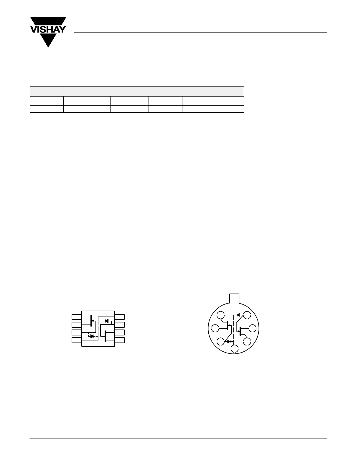
The SST441NL is a monolithic high-speed dual JFET
mounted in a single SO-8 package. This JFET is an excellent
choice for use as wideband differential amplifiers in
demanding test and measurement applications.
Pins 4 and 8 on the SST441NL and pin 4 on the U441NL part
numbers enable the substrate to be connected to a positive,
external bias (V
SUBSTRATE S
) to avoid latchup.
DD
Narrow Body SOIC
S
1
1
D
2
1
G
3
1
4
Marking Codes:
SST441NL - 441NL
Top View
8
7
6
5
SUBSTRATE
G
2
D
2
2
ABSOLUTE MAXIMUM RATINGS
Gate-Drain, Gate-Source Voltage -25 V. . . . . . . . . . . . . . . . . . . . . . . . . . . . . . .
Gate Current 50 mA. . . . . . . . . . . . . . . . . . . . . . . . . . . . . . . . . . . . . . . . . . . . . . . . .
Lead Temperature (
Storage Temperature -55 to 150_C. . . . . . . . . . . . . . . . . . . . . . . . . . . . . . . . . . .
Operating Junction Temperature -55 to 150_C. . . . . . . . . . . . . . . . . . . . . . . . . .
1
/16” from case for 10 sec.) 300_C. . . . . . . . . . . . . . . . . . .
The U441NL in the hermetically sealed TO-78 package is
available with full military processing.
The SO-8 package provides ease of manufacturing. The
symmetrical pinout prevents improper orientation. The SO-8
package is available with tape-and-reel options for
compatibility with automatic assembly methods.
TO-78
S
1
1
D
1
2
3
G
1
Power Dissipation : Per Side
Notes
a. Derate 2.4 mW/_C above 25_C
b. Derate 4 mW/_C above 25_C
4
CASE, SUBSTRATE
Top View
U441NL
Total
G
2
7
D
2
6
5
S
2
a
b
300 mW. . . . . . . . . . . . . . . . . . . . . . . .
500 mW. . . . . . . . . . . . . . . . . . . . . . . . . . .
For applications information see AN102.
Document Number: 72056
S-22526–Rev. A, 17-Feb-03
www.vishay.com
7-1
Page 2
SST441NL/U441NL
S
V
DS
= 10 V, ID = 5 mA
S
VDS = 10 V, ID = 5 mA
S
VDS = 10 V, ID = 5 mA
Vishay Siliconix
New Product
SPECIFICATIONS (TA = 25_C UNLESS OTHERWISE NOTED)
Limits
Parameter Symbol
Test Conditions
Min Typ
Static
Gate-Source Breakdown Voltage V
Gate-Source Cutoff Voltage V
Saturation Drain Current
Gate Reverse Current I
Gate Operating Current I
Gate-Source Forward Voltage V
b
(BR)GSS
GS(off)
I
DSS
GSS
G
GS(F)
IG = -1 mA, VDS = 0 V
VDS = 10 V, ID = 1 nA -1 -3.5 -6
VDS = 10 V, VGS = 0 V 6 15 30 mA
VGS = -15 V, VDS = 0 V -1 -500 pA
TA = 125_C
VDG = 10 V, ID = 5 mA -1 -500 pA
TA = 125_C
IG = 1 mA , VDS = 0 V 0.7 V
-25 -35
Dynamic
Common-Source
Forward Transconductance
Common-Source
Output Conductance
Common-Source
Forward Transconductance
Common-Source
Output Conductance
Common-Source
Input Capacitance
Common-Source
Reverse Transfer Capacitance
Equivalent Input Noise Voltage e
g
fs
g
os
g
fs
g
os
C
iss
C
rss
n
V
= 10 V, I
D
V
= 10 V, ID = 5 mA
D
V
= 10 V, ID = 5 mA
D
VDS = 10 V, ID = 5 mA
= 5 mA
D
f = 1 kHz
f = 100 MHz
f = 1 MHz
f = 10 kHz
4.5 6 9 mS
Matching
Differential Gate-Source Voltage
Gate-Source Voltage Differential
Change with Temperature
Saturation Drain Current Ratio
Transconductance Ratio
Common Mode Rejection Ratio CMRR VDG = 10 to 15 V, ID = 5 mA 90 dB
Notes
a. Typical values are for DESIGN AID ONLY, not guaranteed nor subject to production testing. NNZ
b. Pulse test: PW v300 ms duty cycle v3%.
c. Assumes smaller value in the numerator.
c
c
|
V
GS1–VGS2
|
D
V
GS1–VGS2
DT
I
DSS1
I
DSS2
g
g
fs1
fs2
|
|
VDG = 10 V, ID = 5 mA 7 20 mV
VDG = 10 V, ID = 5 mA
T
= -55 to 125_C
A
VDS = 10 V, VGS = 0 V 0.98
VDS = 10 V, ID = 5 mA
f = 1 kHz
a
Max Unit
-0.2 nA
-0.2 nA
20 200
5.5 mS
30
3.5
1
4
10
0.98
√Hz
mV/_C
V
mS
mS
pF
nV⁄
www.vishay.com
7-2
Document Number: 72056
S-22526–Rev. A, 17-Feb-03
Page 3

SST441NL/U441NL
New Product
TYPICAL CHARACTERISTICS (TA = 25_C UNLESS OTHERWISE NOTED)
Drain Current and Transconductance
25
20
15
vs. Gate-Source Cutoff Voltage
I
@ VDS = 10 V, VGS = 0 V
DSS
@ VDG = 10 V, VGS = 0 V
g
fs
f = 1 kHz
g
fs
10
5
- Saturation Drain Current (mA)
DSS
I
0
0-5-4-2-1
V
- Gate-Source Cutoff Voltage (V) VDG - Drain-Gate Voltage (V)
GS(off)
20
V
Output Characteristics
= -3 V
GS(off)
16
12
8
- Drain Current (mA)I
D
I
4
I
DSS
-3
VGS= 0 V
-0.4 V
-0.8 V
-1.2 V
-1.6 V
15
g
fs
- Forward Transconductance (mS)
13
11
9
7
5
-100 nA
-10 nA
-1 nA
TA = 125_C
-100 pA
- Gate Leakage
G
-10 pA
I
-1 pA
TA = 25_C
-0.1 pA
0151052025
25
20
15
10
- Drain Current (mA)
D
I
5
Gate Leakage Current
1 mA
100 mA
Output Characteristics
V
= -4 V
GS(off)
Vishay Siliconix
IG @ ID = 5 mA
1 mA
100 mA
5 mA
I
@
GSS
125_C
I
@ 25_C
GSS
VGS= 0 V
-0.4 V
-0.8 V
-1.2 V
-1.6 V
-2.0 V
-2.4 V
0
020161284
VDS - Drain-Source Voltage (V)
5
V
Output Characteristics
= -3 V
GS(off)
4
-0.2 V
3
2
- Drain Current (mA)
D
1
0
010.80.60.40.2
VDS - Drain-Source Voltage (V)
Document Number: 72056
S-22526–Rev. A, 17-Feb-03
VGS= 0 V
-2.0 V
-1.2 V
-1.4 V
-1.6 V
-0.6 V
-0.8 V
-1.0 V
-0.4 V
0
012168420
10
V
8
6
4
- Drain Current (mA)
D
I
2
0
010.80.60.40.2
VDS - Drain-Source Voltage (V)
Output Characteristics
= -4 V
GS(off)
VDS - Drain-Source Voltage (V)
-2.8 V
VGS= 0 V
-0.4 V
-0.8 V
-1.2 V
-1.6 V
-2.0 V
-2.4 V
-2.8 V
www.vishay.com
7-3
Page 4

SST441NL/U441NL
Vishay Siliconix
New Product
TYPICAL CHARACTERISTICS (TA = 25_C UNLESS OTHERWISE NOTED)
Gate-Source Differential Voltage
20
V
GS(off)
16
12
8
- Drain Current (mA)
D
I
4
0
0 -1.5-1.0-0.5 -2.0 -2.5
Voltage Differential with Temperature
100
VDG = 10 V
DT
DT
V/ _C
m
()
10
GS2
V
-
t
D
GS1
V
D
Transfer Characteristics
= -3 V
TA = -55_C
25_C
125_C
VGS - Gate-Source Voltage (V) ID - Drain Current (mA)
VDS = 10 V
100
VDG = 10 V
T
A
(mV)
10
GS2
V
GS1
V
1
0.1 1 10
vs. Drain Current
150
= 25 to 125_C
A
= -55 to 25_C
A
130
110
CMRR (dB)
CMRR = 20 log
90
70
vs. Drain Current
= 25_C
Common Mode Rejection Ratio
vs. Drain Current
DVDG = 10 - 20 V
D
DV
DG
V
GS1 VGS2
5 - 10 V
1
0.1 1 10
100
80
60
40
- Voltage Gain
V
A
20
0
www.vishay.com
7-4
I
- Drain Current (mA) ID - Drain Current (mA)
D
Circuit Voltage Gain vs. Drain Current
g
A
V
Assume VDD = 15 V, VDS = 5 V
R
I
D
fsRL
+
1 ) RLg
10 V
+
L
-4 V
- Drain Current (mA)
os
I
D
V
GS(off)
1100.1
= -3 V
50
0.1 1 10
On-Resistance vs. Drain Current
V
= -3 V
GS(off)
-4 V
0.1 1.0 10
ID - Drain Current (mA)
Document Number: 72056
S-22526–Rev. A, 17-Feb-03
- Drain-Source On-Resistance ( Ω )
r
200
160
120
80
40
DS(on)
0
Page 5

SST441NL/U441NL
New Product
TYPICAL CHARACTERISTICS (TA = 25_C UNLESS OTHERWISE NOTED)
- Input Capacitance (pF)C
iss
Common-Source Input Capacitance
10
8
6
4
2
0
0 -16 -20-8-4
50
40
vs. Gate-Source Voltage
f = 1 MHz
VDS = 0 V
5 V
15 V
VGS - Gate-Source Voltage (V)
Output Conductance vs. Drain Current
V
= -3 V VDS = 10 V
GS(off)
- Reverse Feedback Capacitance (pF)C
rss
-12
20
f = 1 kHz
16
Common-Source Reverse Feedback
Capacitance vs. Gate-Source Voltage
5
f = 1 MHz
4
3
VDS = 0 V
2
1
0
0-20-16-8-4
5 V
15 V
VGS - Gate-Source Voltage (V)
Equivalent Input Noise Voltage vs. Frequency
VDS = 10 V
Vishay Siliconix
-12
30
20
- Output Conductance (µS)
10
os
g
0
0.1 1 10
ID - Drain Current (mA)
TA = -55_C
25_C
Common-Source Forward Transconductance
vs. Drain Current
10
V
= -3 V VDS = 10 V
GS(off)
8
6
4
2
- Forward Transconductance (mS)
fs
g
0
0.1 1 10
TA = -55_C
25_C
ID - Drain Current (mA)
125_C
f = 1 kHz
125_C
12
ID @ 10 mA
8
en - Noise Voltage nV / Hz
4
0
VGS = 0 V
10 100 1 k 100 k10 k
f - Frequency (Hz)
On-Resistance and Output Conductance
vs. Gate-Source Cutoff Voltage
r
DS
rDS @ ID = 1 mA, VGS = 0 V
@ VDG = 10 V, VGS = 0 V, f = kHz
g
os
0-3-5-4-2-1
V
- Gate-Source Cutoff Voltage (V)
GS(off)
- Drain-Source On-Resistance ( Ω )
DS(on)
r
250
200
150
100
50
0
100
g
os
os
- Output Conductance ( m
50
S)g
0
Document Number: 72056
S-22526–Rev. A, 17-Feb-03
www.vishay.com
7-5
Page 6

 Loading...