

Datasheet SST39VF1601, SST39VF3201, SST39VF6401, SST39VF1602, SST39VF3202 Datasheet (Silicon Storage Technology)
...Page 1

查询39VF6401供应商
16 Mbit / 32 Mbit / 64 Mbit (x16) Multi-Purpose Flash Plus
SST39VF1601 / SST39VF32 01 / SST39V F64 01
SST39VF1602 / SST39VF32 02 / SST39V F64 02
SST39VF160x / 320x / 640x2.7V 16Mb / 32Mb / 64Mb (x16) MPF+ memories
FEATURES:
• Organized as 1M x16: SST39VF1601/1602
2M x16: SST39VF3201/3202
4M x16: SST39VF6401/6402
• Single Voltage Read and Write Operations
– 2.7-3.6V
• Superior Reliability
– Endurance: 100,000 Cycles (Typical)
– Greater than 100 years Data Retention
• Low Power Consumption (typical values at 5 MHz)
– Active Current: 9 mA (typical)
– Standby Current: 3 µA (typical)
– Auto Low P ower Mode: 3 µA (typical)
• Hardware Block-Protection/WP# Input Pin
– Top Block-Protection (top 32 KWord)
for SST39VF1602/3202/6402
– Bottom Block-Protection (bottom 32 KWord)
for SST39VF1601/3201/6401
• Sector-Erase Capability
– Uniform 2 KWord sectors
• Block-Erase Capability
– Uniform 32 KWord blocks
• Chip-Erase Capability
• Erase-Suspend/Erase-Resume Capabilities
• Hardware Reset Pin (RST#)
Preliminary Specifications
• Security-ID Feature
– SST: 128 bits; User: 128 bits
• Fast Read Access Time:
– 70 ns
– 90 ns
• Latched Address and Data
• Fast Erase and Word-Program:
– Sector-Erase Time: 18 ms (typical)
– Block-Erase Time: 18 ms (typical)
– Chip-Erase Time: 40 ms (typical)
– Word-Program Time: 7 µs (typical)
• Automatic Write Timing
– Internal V
Generation
PP
• End-of-Write Detection
– Toggle Bits
– Data# Polling
• CMOS I/O Compatibility
• JEDEC Standard
– Flash EEPROM Pinouts and command sets
• Packages Available
– 48-lead TSOP (12mm x 20mm)
– 48-ball TFBGA (6mm x 8mm) for 16M and 32M
– 48-ball TFBGA (8mm x 10mm) for 64M
PRODUCT DESCRIPTION
The SST39VF160x/320x/6 40x devices are 1M x16, 2M
x16, and 4M x16 respectively, CMOS Multi-Purpose
Flash Plus (MPF+) manufactured with SST’s proprietar y,
high performance CMOS SuperFlash technology. The
split-gate cell design and thick-oxide tunneling injector
attain better reliability and manufacturability compared
with alternate approaches. The SST39VF160x/320x/640x
write (Program or Erase) with a 2.7 -3.6V power supply.
These devices conform to JEDEC standard pinouts for
x16 memories.
Featuring high performance Word-Program, the
SST39VF160x/ 320x/ 640x d evices provide a typic al WordProgram time of 7 µsec. T hese devices use Toggle Bit or
Data# Polling to indicate the completion of Program operation. To protect against inadvertent write, they have on-chip
hardware and Software Data Protection schemes.
Designed, manufactured, and tested for a wide spectrum of
applications, these d evices are offered with a guaranteed
typical endurance of 100,000 cycles. Data retention is rated
at greater than 100 years.
The SST39VF160x/320x/640x devices are suited for applications that require convenient and economical updating of
program, configuration, or data memory. For all system
applications, they significantly improve performance and
reliability, while lowering power consumption . They inherently use less energy during Erase and Program than alternative flash technologi es. The total energy consum ed is a
function of the applied voltage, current, and time of application. Since for any given voltage range, the SuperFlash
technology uses less current to program and has a shorter
erase time, the total energy consumed during any Erase or
Program operation is l ess than alter native flash technologies. These devices also im prove flexibility while lowering
the cost for program, data, and configuration storage applications.
The SuperFlash technology prov ides fixed Erase and Program times, independent of the n umbe r of Er ase/Prog r am
cycles that have occurred. Therefore the system software
or hardware does not hav e to be modified or de-rated as is
necessary with alternative flash technologies, whose
Erase and Program times increase with accumulated
Erase/Program cycles.
©2003 Silicon Storage Technology, Inc.
S71223-03-000 11/03
1
The SST logo and SuperFlash are registered trademarks of Silicon Storage Technology, Inc.
MPF is a trademark of Silicon Storage Technology, Inc.
These specifications are subject to change without notice.
Page 2

Preliminary Specifications
16 Mbit / 32 Mbit / 64 Mbit Multi-Purpose Flash Plus
SST39VF1601 / SST39VF3201 / SST39VF6401
SST39VF1602 / SST39VF3202 / SST39VF6402
To meet high density, surface mount requirements, the
SST39VF160x/320x/640x are offered in 48-lead TSOP
and 48-ball TFBGA packages. See Figures 1 and 2 for
pin assignments.
Device Operation
Commands are used to initiate the memory operation functions of the device. Commands are written to the device
using standard microprocess or write sequences. A command is written by asse r ting WE# low whil e keeping CE#
low. The address bus is latched on the falling edge of WE#
or CE#, whichever occurs last. T he data bus is latc hed o n
the rising edge of WE# or CE#, whichever occurs first.
The SST39VF160x/320x/640x also have the Auto Low
Power mode which puts the device in a near standby
mode after data has been accessed with a valid Read
operation. This reduces the I
typically 9 mA to typically 3 µA. The Auto Low Power mode
reduces the typical I
mA/MHz of Read cycle time. The d evi ce exit s the A uto Low
Power mode with any address transition or control s ignal
transition used to initiate another Read cycle, with no
access time penal ty. Note that the device does not enter
Auto-Low Power mode after power-up with CE# held
steadily low, until the first address transition or CE# is
driven hi gh.
active re ad cur rent to the ra nge of 2
DD
active read current from
DD
Read
The Read operation of the SST39VF160x/320x/640x is
controlled by C E# and OE#, bot h have to be low for the
system to obtain data from the outputs. CE# is used for
device selection. When CE# is high, the chip is deselected and only standby power is consumed. OE# is the
output control and is used to gate data from the output
pins. The data bus is in high impedance state when
either CE# or OE# is high. Ref e r to the R ead cycl e timing
diagram for further details (Fig ure 3).
Word-Program Operation
The SST39VF160x/320x/640x are programmed on a
word-by-word basis. Before programming, the sector
where the word exists must be ful ly erased. The Program
operation is accom plished in thre e steps. The first step is
the three-byte load sequence for Software Data Protection.
The second step is to load word add ress and word data.
During the Word-Program operation, the addresses are
latched on the falling ed ge of either CE# or WE#, whi chever occurs last. The data i s latched on the r ising edge of
either CE# or WE#, whichever occurs first. The third step is
the interna l Program operation which is initiated after the
rising edge of the fourth WE# or CE#, whichever occurs
first. The Program o peration, once initiated, wil l be completed within 10 µs. See Figures 4 and 5 for WE# and CE#
controlled Pro gram operation timing diagrams a nd Figure
19 for flowcharts. Dur ing the Program operation, th e only
valid reads are Data# Polling and Toggle Bit. Dur ing the
internal Program operation, the host is free to perform additional tasks. Any commands issued during the internal Program operation are ignored. During the command
sequence, WP# should be statically held high or low.
Sector/Block-Erase Operation
The Sector- (or Block-) Erase operation allows the system
to erase the device on a sector-by-sector (or block-byblock) basis. The SST39VF160x/320x/640x offer both Sector-Erase and Block-Erase mode. The sector archi tecture
is based on uniform se ctor size of 2 KWord. The BlockErase mode is bas ed on uniform block size of 32 KWord.
The Sector-Erase op eration is in itiated by executing a sixbyte command sequence with Sector-Erase command
(30H) and sect or address (SA) in the l ast bus cycle. The
Block-Erase operation is initiated by executing a six-byte
command sequence with Block-Erase command (50H)
and block address (BA) in the last bus cycle. The sector or
block address is latched on the falling edge of the sixth
WE# pulse, while the command (30H or 50H) is latched on
the rising edge of th e six th WE# pu lse. The int er na l Eras e
operation begins a fter the sixth WE# pulse. The End -ofErase operation can be determined using either Data#
Polling or Toggle Bit methods. See Figures 9 and 10 for timing waveforms and Figure 23 for the flowchart. Any commands issued during the Sec tor- or B lock-Era se op erat io n
are ignored. When WP# is low, any attempt to Sector(Block-) Erase the prote cted block will be ignor ed. During
the command sequence, WP# should be statically held
high or low.
Erase-Suspend/Erase-Resume Commands
The Erase-Suspend operation temporarily suspends a
Sector- or Block-Erase operation thus allowing data to be
read from any memor y loca tion, or program data into any
sector/block that is not sus pended for an Erase operation .
The operation is executed by issuing one byte command
sequence with Erase-Suspend command (B0H). The
device automatically enters read mode typically within 20
µs after the Era se-Suspend command had been issued.
Valid data can be read from any sector or block that is not
suspended from an Erase operation. Reading at addr ess
location withi n erase-suspende d sectors/blocks will output
DQ
toggling and DQ6 at “1”. While in Erase-Suspend
2
mode, a Word-Program operation is allowed except for the
sector or block selected for Erase-Suspend.
©2003 Silicon Storage Technology, Inc. S71223-03-000 11/03
2
Page 3

16 Mbit / 32 Mbit / 64 Mbit Multi-Purpose Flash Plus
SST39VF1601 / SST39VF3201 / SST39VF6401
SST39VF1602 / SST39VF3202 / SST39VF6402
Preliminary Specifications
T o resume Sector-Erase or Block-Erase operation which has
been suspended the system must issue Erase Resume
command. The operation is executed by issuing one byte
command sequence with Erase Resume command (30H)
at any address in th e last Byte sequence .
Chip-Erase Operation
The SST39VF160x/320x/640x provide a Chip-Er ase operation, which allows the user to erase the entire memory
array to the “1” state. This is useful when the entire device
must be quickly erased.
The Chip-Erase operation is initiated by executing a sixbyte command sequence with Chip-Erase command
(10H) at address 5555H in the last byte sequence. The
Erase operation begins with the rising edge of the sixth
WE# or CE#, whichever occurs first. During the Erase
operation, the only v alid read is Toggle Bit or Data# P olling.
See Table 6 for the command sequence, Figure 9 for timing diagram, and Figure 23 for the flowchart. Any commands issued during the Chip-Erase operation are
ignored. When WP# is low, any attempt to Chip-Erase will
be ignored. During the command sequence, WP# should
be statically held high or lo w.
Write Operation Status Detection
The SST39VF160x/320x/640x provide two software
means to detect the completion of a Write (Program or
Erase) cycle, in ord er to optimize the system wri te cycle
time. The software detection includes two status bits: Data#
Polling (DQ
) and Toggle Bit (DQ6). The End-of-Write
7
detection mode is enabled afte r the rising edge of WE#,
which initiates the internal Program or Erase operation.
The actual completion of the nonvolatile write is asynchronous with the system; therefore, either a Data# Polling or Toggle Bit read may be simultaneous with the
completion of the write cycle. If this occurs, the system
may possibly get an erroneous result, i.e., valid data may
appear to conflict w it h ei th er D Q
or DQ6. In order to pre-
7
vent spurious rejection, if an erroneous result occurs, the
software routine should include a loop to read the
accessed location an additional two (2) times. If both
reads are valid, then the device has completed the Write
cycle, otherwise the reje ction is valid.
Data# Polling (DQ7)
When the SST39VF160x/320x/640x are in the internal
Program operation, any attempt to read DQ
the complement of the true data. Once the Program operation is completed, DQ
even though DQ
7
will produce true data. Note that
7
may have valid data immediately follow-
will produce
7
ing the completion of an internal Write operation, the
remaining data outputs may still be invalid: valid data on the
entire data bus will appear in subsequent successive Read
cycles after a n in te rva l of 1 µ s . Du ring internal Erase operation, any attempt t o rea d DQ
internal Erase operation is completed, DQ
will produce a ‘0’. Once the
7
will produce a
7
‘1’. The Data# P olling is v alid after the rising edge o f f ourth
WE# (or CE#) pulse for Program operation. For Sector-,
Block- or Chip-Erase, the Data# Polling is valid after the
rising edge of sixth WE# (or CE#) pulse. See Figure 6 for
Data# P olling timing diagram an d Figure 20 f or a flowchart.
Toggle Bits (DQ6 and DQ2)
During the inter nal Program or Erase ope ration, any consecutive attempts to read DQ
and “0”s, i.e., toggling between 1 and 0. Wh en the i nte rnal
Program or Erase operat ion is complete d, the DQ
stop toggling. The device is then ready for the next operation. For Sector-, Block-, or Chip-Erase, the toggle bit (DQ
is valid after the ris ing edge of six th WE# (or CE#) p ulse.
DQ
will be set to “1” if a Read operation is attempted on an
6
Erase-Suspended Sector/Block. If Program operation is initiated in a sector/block not selected in Erase-Suspend
mode, DQ
will toggle .
6
An additional Toggle Bit is available on DQ
used in conjunction with DQ
sector is being actively erased or erase-suspended. T able 1
shows detailed status bits information. The Toggle Bit
(DQ
) is valid after the rising edge of the last WE# (or CE#)
2
pulse of Write operation. See Figure 7 for Toggle Bit timing
diagram and Figure 20 for a flowchart.
TABLE 1: WRITE OPERATION STATUS
Status DQ7DQ
Normal
Operation
EraseSuspend
Mode
Note: DQ7 and DQ2 require a valid address when reading
Standard
Program
Standard
Erase
Read from
Erase-Suspended
Sector/Block
Read from
Non- Erase-Suspended
Sector/Block
Program DQ
status information.
will produc e a lt ernat in g “1 ” s
6
bit will
6
, which can be
2
to check w h ethe r a pa rticular
6
DQ
6
DQ7# Toggle No Toggle
0 Toggle Toggle
1 1 Toggle
Data Data Data
# Toggle N/A
7
2
T1.0 1223
)
6
©2003 Silicon Storage Technology, Inc. S71223-03-000 11/03
3
Page 4

Preliminary Specifications
16 Mbit / 32 Mbit / 64 Mbit Multi-Purpose Flash Plus
SST39VF1601 / SST39VF3201 / SST39VF6401
SST39VF1602 / SST39VF3202 / SST39VF6402
Data Protection
The SST39VF160x/320x/640x provide both hardware and
software features to protect nonvolatile data from inadvertent
writes.
Hardware Data Protection
Noise/Glitch Protection: A WE# or CE# pulse of le ss than 5
ns will not init iate a write cycle .
V
Power Up/Down Detection: The Write operation is
DD
inhibited when V
Write Inhibit Mode:
is less than 1.5V.
DD
Forcing OE# low, CE# high, or WE#
high will inhibit the W r ite operation. This prevents inadvertent writes during p ow er-up o r po wer- down.
Hardware Block Protection
The SST39VF1602/3202/6402 support top hardware block
protection, which protects the top 32 KWord block of the
device. The SST39VF1601/3201/6401 support bottom
hardware block protection, which protects the bottom 32
KWord block of the device. The Boot Block address ranges
are descri bed in Table 2. Program an d Erase operations
are prevented on the 32 KWord when WP# is low. If WP# is
left floating, it is internally h eld high via a pull-u p resistor,
and the Boot Block is unp rotected, enabling Program an d
Erase operations on that block.
TABLE 2: B
Product Address Range
Bottom Boot Block
SST39VF1601/3201/6401 000000H-007FFFH
Top Boot Block
SST39VF1602 0F8000H-0FFFFFH
SST39VF3202 1F8000H-1FFFFFH
SST39VF6402 3F8000H-3FFFFFH
OOT BLOCK ADDRESS RANGES
T2.0 1223
Hardware Reset (RST#)
The RST# pin provides a hardware method of resetting the
device to read array data. When the RST# pin is held low
for at least T
any in-progress operation will terminate and
RP,
return to Read mode. When no internal Program/Erase
operation is in progress, a minimum period of T
RHR
is
required after RST# is driven high before a valid Read can
take place (see Figure 15).
The Erase or Program operation that has been interrupted
needs to be reinitiated after the device resumes normal
operation mode to ensure data integrity .
Software Data Protection (SDP)
The SST39VF160x/320x/640x provide the JEDEC
approved Software Data Protection scheme for all data
alteration operations, i.e., Program and Erase. Any Program operation requires the inclusion of the three-byte
sequence. The three-byte load sequence is used to initiate
the Program operation, p roviding optimal protection from
inadvertent Write operations, e.g., during the system
power-up or power-down. Any Erase operation requires the
inclusion of six-byte sequence. These devices are shipped
with the Software Data Protection permanently enabled.
See T ab le 6 for the specific software command codes. During SDP command sequence, invalid commands will abort
the de v ice t o re a d mode w i th in T
DQ
can be VIL or VIH, but no other value, during any SDP
8
The contents of DQ15-
RC.
command sequence.
Common Flash Memory Interface (CFI)
The SST39VF160x/320x/640x also contain the CFI information to describe the characteristics of the device. In
order to enter the CFI Query mode, the system must write
three-byte sequence, same as product ID entry command
with 98H (CFI Query command) to address 5555H in the
last byte sequence. Once the de vice enters the CFI Query
mode, the system can read CFI data at the addresses
given in Tables 7 through 10. The system must write the
CFI Exit command to return to Read mode from the CFI
Query mode.
©2003 Silicon Storage Technology, Inc. S71223-03-000 11/03
4
Page 5

16 Mbit / 32 Mbit / 64 Mbit Multi-Purpose Flash Plus
SST39VF1601 / SST39VF3201 / SST39VF6401
SST39VF1602 / SST39VF3202 / SST39VF6402
Preliminary Specifications
Product Identification
The Product Identificatio n mode id entifies th e devices as
the SST39VF1601, SST39VF1602, SST39VF3201,
SST39VF3202, SST39VF6401, SST39VF6402, and
manufacturer as SST. This mode may be accessed software operations. Users may use the Software Product
Identification operation to identify the par t (i.e., using the
device ID) when using multiple manufacturers in the same
socket. For details, see Table 6 for software operation,
Figure 11 for the Software ID Entry a nd Read tim ing diagram and Figure 21 for the Software ID Entry command
sequence flowchart.
TABLE 3: P
Manufacture r’s ID 0000H BFH
Device ID
SST39VF1601 0001H 234BH
SST39VF1602 0001H 234AH
SST39VF3201 0001H 235BH
SST39VF3202 0001H 235AH
SST39VF6401 0001H 236BH
SST39VF6402 0001H 236AH
RODUCT IDENTIFICATION
Address Data
T3.2 1223
Security ID
The SST39VF160x/320x/640x devices offer a 256-bit
Security ID space. The Secure ID space is divided into two
128-bit segment s - one factory programmed seg ment an d
one user programmed seg ment. The first segment is programmed and locked at SS T with a ra ndom 128-bi t number. The user segment is left un-programmed for the
customer to program as desired.
To program the user segm ent of the Security ID, the user
must use the Security ID Word-Program command. To
detect end-of-write for the SEC ID, read the toggle bits. Do
not use Data# Polling. Once this is complet e, the Sec ID
should be locked using the User Sec ID Program Lock-Out.
This disables any future corr up ti on of this sp ac e. Note tha t
regardless of whether or not the Sec ID is locked, neither
Sec ID segment can be erased.
The Secure ID space can be queried by executing a threebyte command sequence with Enter Sec ID command
(88H) at address 5555H in th e last byte sequence. To exit
this mode, the Exit Sec ID command should be executed.
Refer to Table 6 for more details.
Product Identification Mode Exit/
CFI Mode Exit
In order to return to the standard Read mode, the Software
Product Identific ation mode must be exited. Exit is acco mplished by issuing the Software ID Exit command
sequence, which returns the device to the Read mode.
This command may also be used to reset the device to the
Read mode after any inadvertent transient condition that
apparently caus es the device to behave abnor mally, e.g. ,
not read correct ly. Please note th at the Software ID Exit/
CFI Exit command is ignored during an internal Program or
Erase operation. See Table 6 for software command
codes, Figure 13 for timing waveform, and Figures 21 and
22 for flowcharts.
©2003 Silicon Storage Technology, Inc. S71223-03-000 11/03
5
Page 6

Preliminary Specifications
FUNCTIONAL BLOCK DIAGRAM
16 Mbit / 32 Mbit / 64 Mbit Multi-Purpose Flash Plus
SST39VF1601 / SST39VF3201 / SST39VF6401
SST39VF1602 / SST39VF3202 / SST39VF6402
Memory Address
SST39VF6401/6402
A15
A14
A13
A12
A11
A10
A9
A8
A19
A20
WE#
RST#
A21
WP#
NC
A18
A17
A7
A6
A5
A4
A3
A2
A1
CE#
OE#
WE#
WP#
RESET#
SST39VF3201/3202
A15
A14
A13
A12
A11
A10
A9
A8
A19
A20
WE#
RST#
NC
WP#
NC
A18
A17
A7
A6
A5
A4
A3
A2
A1
Address Buffer & Latches
Control Logic
SST39VF1601/1602
A15
A14
A13
A12
A11
A10
A9
A8
A19
NC
WE#
RST#
NC
WP#
NC
A18
A17
A7
A6
A5
A4
A3
A2
A1
1
2
3
4
5
6
7
8
9
10
11
12
13
14
15
16
17
18
19
20
21
22
23
24
X-Decoder
Standard Pinout
T op Vie w
Die Up
SuperFlash
Memory
Y-Decoder
I/O Buffers and Data Latches
DQ15 - DQ
1223 48-tsop P01.3
0
1223 B1.0
SST39VF160x/320x/640x
48
47
46
45
44
43
42
41
40
39
38
37
36
35
34
33
32
31
30
29
28
27
26
25
A16
NC
V
SS
DQ15
DQ7
DQ14
DQ6
DQ13
DQ5
DQ12
DQ4
V
DD
DQ11
DQ3
DQ10
DQ2
DQ9
DQ1
DQ8
DQ0
OE#
V
SS
CE#
A0
FIGURE 1: PIN ASSIGNMENTS FOR 48-LEAD TSOP
©2003 Silicon Storage Technology, Inc. S71223-03-000 11/03
6
Page 7

16 Mbit / 32 Mbit / 64 Mbit Multi-Purpose Flash Plus
SST39VF1601 / SST39VF3201 / SST39VF6401
SST39VF1602 / SST39VF3202 / SST39VF6402
Preliminary Specifications
TOP VIEW (balls facing down)
SST39VF1601/1602
6
A13
5
4
3
2
1
A9
WE#
NC
A7
A3
A12
A8
RST#
WP#
A17
A4
A14
A10
NC
A18
A6
A2
A15
A11
A19
NC
A5
A1
A16
DQ7
DQ5
DQ2
DQ0
A0
NC
DQ14
DQ12
DQ10
DQ8
CE#
DQ15
DQ13
V
DD
DQ11
DQ9
OE#
V
SS
DQ6
DQ4
DQ3
DQ1
V
SS
1223 48-tfbga B3K P02.0
6
5
4
3
2
1
A B C D E F G H
TOP VIEW (balls facing down)
SST39VF3201/3202
A14
A15
A16
DQ7
DQ5
DQ2
DQ0
A0
NC
DQ14
DQ12
DQ10
DQ8
CE#
A13
A9
WE#
NC
A7
A3
A12
A8
RST#
WP#
A17
A4
A10
NC
A18
A6
A2
A11
A19
A20
A5
A1
A B C D E F G H
DQ15
DQ13
V
DD
DQ11
DQ9
OE#
V
SS
DQ6
DQ4
DQ3
DQ1
V
SS
1223 48-tfbga B3K P02a.2
TOP VIEW (balls facing down)
SST39VF6401/6402
6
5
4
3
2
1
A13
A9
WE#
NC
A7
A3
A12
A8
RST#
WP#
A17
A4
A14
A10
A21
A18
A6
A2
A15
A11
A19
A20
A5
A1
A16
DQ7
DQ5
DQ2
DQ0
A0
NC
DQ14
DQ12
DQ10
DQ8
CE#
DQ15
DQ13
V
DD
DQ11
DQ9
OE#
V
SS
DQ6
DQ4
DQ3
DQ1
V
SS
A B C D E F G H
1223 4-tfbga B1K P02b.2
FIGURE 2: PIN ASSIGNMENTS FOR 48-BALL TFBGA
©2003 Silicon Storage Technology, Inc. S71223-03-000 11/03
7
Page 8

16 Mbit / 32 Mbit / 64 Mbit Multi-Purpose Flash Plus
SST39VF1601 / SST39VF3201 / SST39VF6401
SST39VF1602 / SST39VF3202 / SST39VF6402
Preliminary Specifications
TABLE 4: PIN DESCRIPTION
Symbol Pin Name Functions
1
-A
A
MS
-DQ
DQ
15
WP# Write Protect To protect the top/bottom boot block from Erase/Program operation when grounded.
RST# Reset To reset and return the device to Read mod e .
CE# Chip Enable To activate the device when CE# is low.
OE# Output Enable To gate the data output buffers.
WE# Write Enable To control the Write operations.
V
DD
V
SS
NC No Connection Unconnected pins.
1. AMS = Most significant address
A
MS
Address Inputs To provide memory addresses.
0
During Sector-Erase A
During Block-Erase A
Data Input/output T o outpu t d ata during Read cycles and rece ive input data during Write cycles.
0
MS-A15
address lines will select the sector.
MS-A11
address lines will select the block.
Data is internally latched during a Write cycle.
The outputs are in tri-state when OE# or CE# is high.
Power Supply To provide power supply voltage: 2.7-3.6V
Ground
= A19 for SST39VF1601/1602, A20 for SST39VF3201/3202, and A21 for SST39VF6401/6402
T4.2 1223
TABLE 5: OPERATION MODES SELECTION
Mode CE# OE# WE# DQ Address
Read V
Program V
Erase V
Standby V
IL
IL
IL
IH
Write Inhibit X V
XXV
Product Identification
Software Mode V
1. X can be VIL or VIH, but no other value.
IL
V
IL
V
IH
V
IH
X X High Z X
IL
V
IL
V
V
V
D
IH
IL
IL
D
X
OUT
IN
1
X High Z/ D
High Z/ D
IH
V
IH
OUT
OUT
A
IN
A
IN
Sector or block ad dress,
XXH for Chip-Erase
X
X
See Table 6
T5.0 1223
©2003 Silicon Storage Technology, Inc. S71223-03-000 11/03
8
Page 9

16 Mbit / 32 Mbit / 64 Mbit Multi-Purpose Flash Plus
SST39VF1601 / SST39VF3201 / SST39VF6401
SST39VF1602 / SST39VF3202 / SST39VF6402
Preliminary Specifications
TABLE 6: SOFTWARE COMMAND SEQUENCE
Command
Sequence
Word-Program
Sector-Erase
Block-Erase
Chip-Erase
Erase-Suspend
Erase-Resume
Query Sec ID
User Security ID
Word-Program
User Security ID
Program Lock-Out
Software ID En try
CFI Query Entry
Software ID Exit
/CFI Exit/Sec ID Exit
Software ID Ex i t
/CFI Exit/Sec ID Exit
1. Address format A14-A0 (Hex).
2. DQ
3. WA = Program Word address
4. SA
5. With A
6. Valid Word-Addresses for Sec ID are from 000000H-000007H and 000010H-000017H.
7. The device does not remain in Software Product ID Mode if powered down.
8. With A
9. Both Software ID Exit operations are equivalent
10. If users never lock after programming, Sec ID can be programmed over the previously unprogrammed bits (data=1) using the Sec ID
5
7,8
9,10
9,10
Addresses A
Addresses A
Addresses A
15
for Sector-Erase; uses AMS-A11 address lines
X
BA
, for Block-Erase; uses AMS-A15 address lines
X
A
= Most significant address
MS
A
= A19 for SST39VF1601/1602, A20 for SST39VF3201/3202, and A21 for SST39VF6401/6402
MS
15-A19
15-A20
15
-DQ8 can be VIL or VIH, but no other value, for Command sequence
= 0; Sec ID is read with A3-A0,
MS-A4
Lock Status is read with A
=0; SST Manufacturer ID = 00BFH, is read with A0 = 0,
MS-A1
A
= Most significant address
MS
A
= A19 for SST39VF1601/1602, A20 for SST39VF3201/3202, and A21 for SST39VF6401/6402
MS
mode again (the programmed “0” bits cannot be reversed to “1”). Valid Word-Addresses for Sec ID are from 000000H-000007H and
000010H-000017H.
1st Bus
Write Cycle
1
Addr
Data2Addr1Data2Addr1Data2Addr1Data2Addr1Data2Addr1Data
5555H AAH 2AAAH 55H 5555H A0H WA
5555H AAH 2AAAH 55H 5555H 80H 5555H AAH 2AAAH 55H SA
5555H AAH 2AAAH 55H 5555H 80H 5555H AAH 2AAAH 55H BA
2nd Bus
Write Cycle
3rd Bus
Write Cycle
4th Bus
Write Cycle
3
Data
5th Bus
Write Cycle
6th Bus
Write Cycle
4
X
4
X
5555H AAH 2AAAH 55 H 5555H 80H 5555H AAH 2AAAH 55H 5555H 10H
XXXXH B0H
XXXXH 30H
5555H AAH 2AAAH 55 H 5555H 88H
5555H AAH 2AAAH 55H 5555H A5H WA
6
Data
5555H AAH 2AAAH 55H 5555H 85H XXH60000H
5555H AAH 2AAAH 55 H 5555H 90H
5555H AAH 2AAAH 55 H 5555H 98H
5555H AAH 2AAAH 55H 5555H F0H
XXH F0H
can be VIL or VIH, but no other value, for Command sequence for SST39VF1601/1602,
can be VIL or VIH, but no other value, for Command sequence for SST39VF3201/3202,
- A21 can be VIL or VIH, but no other value, for Command sequence for SST39VF6401/6402.
SST ID is read with A
User ID is read with A
= 0000FFH. Unlocked: DQ3 = 1 / Locked: DQ3 = 0.
7-A0
SST39VF1601 Device ID = 234BH, is read with A
SST39VF1602 Device ID = 234AH, is read with A
SST39VF3201 Device ID = 235BH, is read with A
SST39VF3202 Device ID = 235AH, is read with A
SST39VF6401 Device ID = 236BH, is read with A
SST39VF6402 Device ID = 236AH, is read with A
= 0 (Address range = 000000H to 000007H),
3
= 1 (Address range = 000010H to 000017H).
3
= 1,
0
= 1,
0
= 1,
0
= 1,
0
= 1,
0
= 1.
0
2
30H
50H
T6.6 1223
©2003 Silicon Storage Technology, Inc. S71223-03-000 11/03
9
Page 10

16 Mbit / 32 Mbit / 64 Mbit Multi-Purpose Flash Plus
SST39VF1601 / SST39VF3201 / SST39VF6401
SST39VF1602 / SST39VF3202 / SST39VF6402
Preliminary Specifications
TABLE 7: CFI QUERY IDENTIFICATION STRING1 FOR SST39VF16 0X/320X/640X
Address Data Data
10H 0051H Query Unique ASCII string “QRY”
11H 0052H
12H 0059H
13H 0001H Primary OEM command set
14H 0007H
15H 0000H Address for Primary Extended Table
16H 0000H
17H 0000H Alternate OEM command set (00H = none exists)
18H 0000H
19H 0000H Address for Alternate OEM extended Table (00H = none exits)
1AH 0000H
1. Refer to CFI publication 100 for more details.
TABLE 8: SYSTEM INTERFACE INFORMATION FOR SST39VF 160X/320X/640X
Address Data Data
1BH 0027H V
1CH 0036H VDD Max (Program/Erase)
1DH 0000H VPP min. (00H = no VPP pin)
1EH 0000H VPP max. (00H = no VPP pin)
1FH 0003H Typical time out for Word-Program 2
20H 0000H Typical time out for min. size buffer program 2N µs (00H = not supported)
21H 0004H T ypic al time out for individual Sector/Block-Erase 2N ms (24 = 16 ms)
22H 0005H T y pic al time out for Chip-Erase 2
23H 0001H Maximum time out for Word-Program 2N times typical (21 x 23 = 16 µs)
24H 0000H Maximum time out for buffer program 2N times typical
25H 0001H Maximum time out for individual Sector/Block-Erase 2
26H 0001H Maximum time out for Chip-Erase 2N times typical (21 x 25 = 64 ms)
Min (Program/Erase)
DD
DQ7-DQ4: Volts, DQ3-DQ0: 100 millivolts
DQ
-DQ4: Volts, DQ3-DQ0: 100 millivolts
7
N
µs (23 = 8 µs)
N
ms (25 = 32 ms)
N
times typica l (21 x 24 = 32 ms)
T7.1 1223
T8.3 1223
TABLE 9: DEVICE GEOMETRY INFORMATION FOR SST39VF1601/1602
Address Data Data
27H 0015H Device size = 2
28H 0001H Flash Device Interface description; 0001H = x16-only asynchronous interface
29H 0000H
2AH 0000H Maximum number of byte in multi-byte write = 2
2BH 0000H
2CH 0002H Number of Erase Sector/Block sizes supported by device
2DH 00FFH Sector Information (y + 1 = Number of sectors; z x 256B = sector size)
2EH 0001H y = 511 + 1 = 512 sectors (01FF = 511
2FH 0010H
30H 0000H z = 16 x 256 Bytes = 4 KByte/sector (0010H = 16)
31H 001FH Block Information (y + 1 = Number of blocks; z x 256B = block size)
32H 0000H y = 31 + 1 = 32 blocks (001F = 31)
33H 0000H
34H 0001H z = 256 x 256 Bytes = 64 KByte/block (0100H = 256)
©2003 Silicon Storage Technology, Inc. S71223-03-000 11/03
N
Bytes (15H = 21; 221 = 2 MByte)
10
N
(00H = not supported)
T9.0 1223
Page 11
16 Mbit / 32 Mbit / 64 Mbit Multi-Purpose Flash Plus
SST39VF1601 / SST39VF3201 / SST39VF6401
SST39VF1602 / SST39VF3202 / SST39VF6402
TABLE 10: DEVICE GEOMETRY INFORMATION FOR SST39VF3201 /3202
Address Data Data
27H 0016H Device size = 2
28H 0001H Flash Device Interface description; 0001H = x16-only asynchronous interface
29H 0000H
2AH 0000H Maximum number of byte in multi-byte write = 2
2BH 0000H
2CH 0002H Number of Erase Sector/Block sizes supported by device
2DH 00FFH Sector Information (y + 1 = Number of sectors; z x 256B = sector size)
2EH 0003H y = 1023 + 1 = 1024 (03FFH = 1023)
2FH 0010H
30H 0000H z = 16 x 256 Bytes = 4 KBytes/sector (0010H = 16)
31H 003FH Block Information (y + 1 = Number of blocks; z x 256B = block size)
32H 0000H y = 63 + 1 = 64 blocks (003FH = 63)
33H 0000H
34H 0001H z = 256 x 256 Bytes = 64 KBytes/block (0100H = 256)
TABLE 11: DEVICE GEOMETRY INFORMATION FOR SST39VF6401 /6402
Address Data Data
27H 0017H Device size = 2
28H 0001H Flash Device Interface description; 0001H = x16-only asynchronous interface
29H 0000H
2AH 0000H Maximum number of bytes in multi-byte write = 2
2BH 0000H
2CH 0002H Number of Erase Sector/Block sizes supported by device
2DH 00FFH Sector Information (y + 1 = Number of sectors; z x 256B = sector size)
2EH 0007H y = 2047 + 1 = 2048 sectors (07FFH = 2047)
2FH 0010H
30H 0000H z = 16 x 256 Bytes = 4 KBytes/sector (0010H = 16)
31H 007FH Block Information (y + 1 = Number of blocks; z x 256B = block size)
32H 0000H y =127 + 1 = 128 blocks (007FH = 127)
33H 0000H
34H 0001H z = 256 x 256 Bytes = 64 KBytes/block (0100H = 256)
N
Bytes (16H = 22; 222 = 4 MByte)
N
Bytes (17H = 23; 223 = 8 MByte)
N
(00H = not supported)
N
(00H = not supported)
Preliminary Specifications
T10.2 1223
T11.2 1223
©2003 Silicon Storage Technology, Inc. S71223-03-000 11/03
11
Page 12

16 Mbit / 32 Mbit / 64 Mbit Multi-Purpose Flash Plus
SST39VF1601 / SST39VF3201 / SST39VF6401
SST39VF1602 / SST39VF3202 / SST39VF6402
Preliminary Specifications
Absolute Maximum Stress Ratings (Applied conditions greater than those listed under “Absolute Maximum
Stress Ratings” may cause pe r manent dama ge to the device. This is a stres s rating only and funct ional operatio n
of the device at these conditions or conditions greater tha n those defined in the ope rational sections of this data
sheet is not implied. Exposure to absolute maximum stress rating conditions may affect device reliability.)
Temperature Under Bias . . . . . . . . . . . . . . . . . . . . . . . . . . . . . . . . . . . . . . . . . . . . . . . . . . . . . . . . . -55°C to +125°C
Storage Temperature . . . . . . . . . . . . . . . . . . . . . . . . . . . . . . . . . . . . . . . . . . . . . . . . . . . . . . . . . . . -65°C to +150°C
D. C. Voltage on Any Pin to Ground Potential . . . . . . . . . . . . . . . . . . . . . . . . . . . . . . . . . . . . . . . .-0.5V to V
Transient Voltage (<20 ns) on Any Pin to Ground Potential . . . . . . . . . . . . . . . . . . . . . . . . . . . . .-2.0V to V
Voltage on A
Pin to Ground Potential . . . . . . . . . . . . . . . . . . . . . . . . . . . . . . . . . . . . . . . . . . . . . . . . -0.5V to 13.2V
9
Package Power Dissipation Capability (Ta = 25°C) . . . . . . . . . . . . . . . . . . . . . . . . . . . . . . . . . . . . . . . . . . . . . . 1.0W
Surface Mount Lead Soldering Temperature (3 Seconds) . . . . . . . . . . . . . . . . . . . . . . . . . . . . . . . . . . . . . . . 240°C
Output Short Circ uit Curr ent
1. Outputs shorted for no more than one second. No more than one output shorted at a time.
1
. . . . . . . . . . . . . . . . . . . . . . . . . . . . . . . . . . . . . . . . . . . . . . . . . . . . . . . . . . . . . 50 mA
OPERATING RANGE
Range Ambient Temp V
Commercial
Industrial
0°C to +70°C
-40°C to +85°C
DD
2.7-3.6V
2.7-3.6V
DD
DD
+0.5V
+2.0V
AC CONDITIONS OF TEST
Input Rise/Fall Time . . . . . . . . . . . . . . 5 ns
Output Load . . . . . . . . . . . . . . . . . . . . C
See Figures 17 and 18
= 30 pF
L
©2003 Silicon Storage Technology, Inc. S71223-03-000 11/03
12
Page 13

16 Mbit / 32 Mbit / 64 Mbit Multi-Purpose Flash Plus
SST39VF1601 / SST39VF3201 / SST39VF6401
SST39VF1602 / SST39VF3202 / SST39VF6402
TABLE 12: DC OPERATING CHARACTERISTICS VDD = 2.7-3.6V
Limits
Symbol Parameter
I
DD
I
SB
I
ALP
I
LI
I
LIW
I
LO
V
IL
V
ILC
V
IH
V
IHC
V
OL
V
OH
1. Typical conditions for the Active Current shown on the front page of the data sheet are average values at 25°C
2. See Figure 17
3. The I
Power Supply Current Address input=V
3
Read
Program and Erase 35 mA CE#=WE#=VIL, OE#=V
Standby VDD Current 20 µA CE#=V
Auto Low Power 20 µA CE#=V
Input Leakage Current 1 µA VIN=GND to VDD, VDD=VDD Max
Input Leakage Current
on WP# pin and RST#
Output Leakage Current 10 µA V
Input Low Voltage 0.8 V VDD=VDD Min
Input Low Voltage (CMOS) 0.3 V VDD=VDD Max
Input High Voltage 0.7V
DD
Input High Voltage (CMOS) VDD-0.3 V VDD=VDD Max
Output Low Voltage 0.2 V IOL=100 µA, VDD=VDD Min
Output High Voltage VDD-0.2 V IOH=-100 µA, VDD=VDD Min
(room temperature), and V
current listed is typically less than 2mA/MHz, with OE# at V
DD
= 3V. Not 100% tested.
DD
1
Test ConditionsMin Max Units
V
DD=VDD
Max
18 mA CE#=VIL, OE#=WE#=VIH, all I/Os open
IHC
ILC
All inputs=V
10 µA WP#=GND to VDD or RST#=GND to V
=GND to VDD, VDD=VDD Max
OUT
VVDD=VDD Max
Typical VDD is 3V.
IH.
Preliminary Specifications
2
WE#=V
DD,
IH
, at f=5 MHz,
IHC
T12.8 1223
IL T/VIHT
, VDD=VDD Max
, VDD=VDD Max
or V
SS
DD
TABLE 13: RECOMMENDED SYSTEM POWER-UP TIMINGS
Symbol Parameter Minimum Units
T
PU-READ
T
PU-WRITE
1
1
1. This parameter is measured only for initial qualification and after a design or process change that could affect this parameter.
Power-up to Read Operation 100 µs
Power-up to Program/Erase Operation 100 µs
TABLE 14: CAPACITANCE (Ta = 25°C, f=1 Mhz, other pins open)
Parameter Description Test Condition Maximum
1
C
I/O
1
C
IN
1. This parameter is measured only for initial qualification and after a design or process change that could affect this parameter.
I/O Pin Capacitance V
= 0V 12 pF
I/O
Input Capacitance VIN = 0V 6 pF
TABLE 15: RELIABILITY CHARACTERISTICS
Symbol Parameter Minimum Specification Units Test Method
1,2
N
END
1
T
DR
1
I
LTH
1. This parameter is measured only for initial qualification and after a design or process change that could affect this parameter.
2. N
endurance rating is qualified as a 10,000 cycle minimum for the whole device. A sector- or block-level rat ing would result in a
END
higher minimum specification.
Endurance 10,000 Cycles JEDEC Standard A117
Data Retention 100 Years JEDEC Standard A103
Latch Up 100 + I
DD
mA JEDEC Standard 78
T13.0 1223
T14.0 1223
T15.2 1223
©2003 Silicon Storage Technology, Inc. S71223-03-000 11/03
13
Page 14

16 Mbit / 32 Mbit / 64 Mbit Multi-Purpose Flash Plus
SST39VF1601 / SST39VF3201 / SST39VF6401
SST39VF1602 / SST39VF3202 / SST39VF6402
Preliminary Specifications
AC CHARACTERISTICS
TABLE 16: READ CYCLE TIMING PARAMETERS VDD = 2.7-3.6V
SST39VFxx01/xx02-70 SST39VFxx01/xx02-90
Symbol Parameter
T
RC
T
CE
T
AA
T
OE
T
CLZ
T
OLZ
T
CHZ
T
OHZ
1
T
OH
1
T
RP
T
RHR
1,2
T
RY
1. This parameter is measured only for initial qualification and after a design or process change that could affect this parameter.
2. This parameter applies to Sector-Erase, Block-Erase and Program operations.
Read Cycle Time 70 90 ns
Chip Enable Access Time 70 90 ns
Address Access Time 70 90 ns
Output Enable Access Time 35 45 ns
1
CE# Low to Active Output 0 0 ns
1
OE# Low to Active Output 0 0 ns
1
CE# High to High-Z Output 20 30 ns
1
OE# High to High-Z Output 20 30 ns
Output Hold from Address Change 0 0 ns
RST# Pulse Width 500 500 ns
1
RST# High before Read 50 50 ns
RST# Pin Low to Read Mode 20 20 µs
This parameter does not apply to Chip-Erase operations.
UnitsMin Max Min Max
T16.3 1223
TABLE 17: PROGRAM/ERASE CYCLE TIMIN G PARAMETERS
Symbol Parameter Min Max Units
T
BP
T
AS
T
AH
T
CS
T
CH
T
OES
T
OEH
T
CP
T
WP
T
WPH
T
CPH
T
DS
T
DH
T
IDA
T
SE
T
BE
T
SCE
1. This parameter is measured only for initial qualification and after a design or process change that could affect this parameter.
Word-Program Time 10 µs
Address Setup Time 0 ns
Address Hol d Time 30 ns
WE# and CE# Setup Time 0 ns
WE# and CE# Hold Time 0 ns
OE# High Setup Time 0 ns
OE# High Hold Time 10 ns
CE# Pulse Width 40 ns
WE# Pulse Width 40 ns
1
WE# Pulse Width High 30 ns
1
CE# Pulse Width High 30 ns
Data Setup Time 30 ns
1
Data Hold Time 0 ns
1
Software ID Access and Exit Time 150 ns
Sector-Erase 25 ms
Block-Erase 25 ms
Chip-Erase 50 ms
T17.1 1223
©2003 Silicon Storage Technology, Inc. S71223-03-000 11/03
14
Page 15

16 Mbit / 32 Mbit / 64 Mbit Multi-Purpose Flash Plus
SST39VF1601 / SST39VF3201 / SST39VF6401
SST39VF1602 / SST39VF3202 / SST39VF6402
Preliminary Specifications
ADDRESS A
MS-0
CE#
OE#
IH
WE#
DQ
15-0
HIGH-Z
Note: AMS = Most significant address
= A19 for SST39VF1601/1602, A20 for SST39VF3201/3202, and A21 for SST39VF6401/6402
A
MS
FIGURE 3: READ CYCLE TIMING DIAGRAM
T
T
OLZV
CLZ
T
RC
T
CE
T
OE
T
AA
T
OHZ
T
T
OH
CHZ
HIGH-Z
DAT A V ALIDDAT A V ALID
1223 F03.2
ADDRESS A
MS-0
5555 2AAA 5555 ADDR
T
AH
T
WP
WE#
T
AS
T
WPH
T
DS
OE#
T
CH
CE#
T
CS
DQ
15-0
XXAA XX55 XXA0 DATA
SW0 SW1 SW2
WORD
(ADDR/DATA)
Note: AMS = Most significant address
AMS = A
WP# must be held in proper logic state (V
X can be V
for SST39VF1601/1602, A20 for SST39VF3201/3202, and A21 for SST39VF6401/6402
19
but no other value
or V
IL
IH,
or VIH) 1 µs prior to and 1 µs after the command sequence
IL
FIGURE 4: WE# CONTROLLED PROGRAM CYCLE TIMI N G DIAGRAM
INTERNAL PROGRAM OPERATION STARTS
T
BP
T
DH
1223 F04.3
©2003 Silicon Storage Technology, Inc. S71223-03-000 11/03
15
Page 16

Preliminary Specifications
ADDRESS A
DQ
MS-0
CE#
OE#
WE#
15-0
T
AS
16 Mbit / 32 Mbit / 64 Mbit Multi-Purpose Flash Plus
SST39VF1601 / SST39VF3201 / SST39VF6401
SST39VF1602 / SST39VF3202 / SST39VF6402
5555 2AAA 5555 ADDR
T
AH
T
CP
T
T
CPH
T
CH
T
CS
XXAA XX55 XXA0 DATA
DS
INTERNAL PROGRAM OPERATION STARTS
T
BP
T
DH
SW0 SW1 SW2
WORD
(ADDR/DATA)
Note: AMS = Most significant address
= A19 for SST39VF1601/1602, A20 for SST39VF3201/3202, and A21 for SST39VF6401/6402
A
MS
WP# must be held in proper logic state (V
X can be V
IL
or V
IH,
but no other value
or VIH) 1 µs prior to and 1 µs after the command sequence
IL
FIGURE 5: CE# CONTROLLED PROGRAM CYCLE TIMING DIAGRAM
ADDRESS A
MS-0
CE#
OE#
WE#
T
OEH
T
CE
T
OE
1223 F05.3
T
OES
DQ
7
Note: AMS = Most significant address
DATA DATA# DATA# DATA
= A19 for SST39VF1601/1602, A20 for SST39VF3201/3202, and A21 for SST39VF6401/6402
A
MS
1223 F06.2
FIGURE 6: DATA# POLLING TIMING D IAGRAM
©2003 Silicon Storage Technology, Inc. S71223-03-000 11/03
16
Page 17

16 Mbit / 32 Mbit / 64 Mbit Multi-Purpose Flash Plus
SST39VF1601 / SST39VF3201 / SST39VF6401
SST39VF1602 / SST39VF3202 / SST39VF6402
Preliminary Specifications
ADDRESS A
MS-0
CE#
OEH
OE#
WE#
DQ
and DQ
6
2
Note: AMS = Most significant address
A
= A19 for SST39VF1601/1602, A20 for SST39VF3201/3202, and A21 for SST39VF6401/6402
MS
FIGURE 7: TOGGLE BITS TIMING DIAGRAM
T
CE
T
T
OET
TWO READ CYCLES
WITH SAME OUTPUTS
OES
1223 F07.3
ADDRESS A
DQ
MS-0
CE#
OE#
WE#
15-0
SIX-BYTE CODE FOR CHIP-ERASE
5555 2AAA 2AAA5555 5555
T
WP
5555
XX55 XX10XX55XXAA XX80 XXAA
SW0 SW1 SW2 SW3 SW4 SW5
Note: This device also supports CE# controlled Chip-Erase operation. The WE# and CE# signals are
interchageable as long as minimum timings are met. (See Table 17)
= Most significant address
A
MS
= A19 for SST39VF1601/1602, A20 for SST39VF3201/3202, and A21 for SST39VF6401/6402
A
MS
WP# must be held in proper logic state (V
X can be V
IL
or V
IH,
but no other value
) 1 µs prior to and 1 µs after the command sequence
IH
T
SCE
1223 F08.4
FIGURE 8: WE# CONTROLLED CHIP-ERASE TIMING DIAGRAM
©2003 Silicon Storage Technology, Inc. S71223-03-000 11/03
17
Page 18

Preliminary Specifications
16 Mbit / 32 Mbit / 64 Mbit Multi-Purpose Flash Plus
SST39VF1601 / SST39VF3201 / SST39VF6401
SST39VF1602 / SST39VF3202 / SST39VF6402
T
SIX-BYTE CODE FOR BLOCK-ERASE
BE
ADDRESS A
MS-0
5555 2AAA 2AAA5555 5555
CE#
OE#
T
WP
WE#
DQ
15-0
SW0 SW1 SW2 SW3 SW4 SW5
Note: This device also supports CE# controlled Block-Erase operation. The WE# and CE# signals are
interchageable as long as minimum timings are met. (See Table 17)
= Block Address
BA
X
= Most significant address
A
MS
= A19 for SST39VF1601/1602, A20 for SST39VF3201/3202, and A21 for SST39VF6401/6402
A
MS
WP# must be held in proper logic state (V
X can be V
IL
or V
IH,
but no other value
or VIH) 1 µs prior to and 1 µs after the command sequence
IL
FIGURE 9: WE# CONTROLLED BLOCK-ERASE TIMING DIAGRAM
BA
X
XX55 XX50XX55XXAA XX80 XXAA
1223 F09.4
SIX-BYTE CODE FOR SECTOR-ERASE
ADDRESS A
MS-0
5555 2AAA 2AAA5555 5555
CE#
OE#
T
WP
WE#
DQ
15-0
SW0 SW1 SW2 SW3 SW4 SW5
Note: This device also supports CE# controlled Sector-Erase operation. The WE# and CE# signals are
interchageable as long as minimum timings are met. (See Table 17)
= Sector Address
SA
X
= Most significant address
A
MS
= A19 for SST39VF1601/1602, A20 for SST39VF3201/3202, and A21 for SST39VF6401/6402
A
MS
WP# must be held in proper logic state (V
X can be V
or VIH, but no other value
IL
or VIH) 1 µs prior to and 1 µs after the command sequence
IL
FIGURE 10: WE# CONTROLLED SECTOR-ERASE TIMING DIAGRAM
T
SE
SA
X
XX55 XX30XX55XXAA XX80 XXAA
1223 F10.4
©2003 Silicon Storage Technology, Inc. S71223-03-000 11/03
18
Page 19

16 Mbit / 32 Mbit / 64 Mbit Multi-Purpose Flash Plus
SST39VF1601 / SST39VF3201 / SST39VF6401
SST39VF1602 / SST39VF3202 / SST39VF6402
Three-Byte Sequence for Software ID Entry
Preliminary Specifications
ADDRESS A
14-0
5555 2AAA 5555 0000 0001
CE#
OE#
T
WP
WE#
T
WPH
DQ
15-0
XX55XXAA XX90
SW0 SW1 SW2
Note: Device ID = 234BH for 39VF1601, 234AH for 39VF1602, 235BH for 39VF3201, 235AH for 39VF3202,
236BH for 39VF6401, and 236AH for 39VF6402,
WP# must be held in proper logic state (V
X can be V
IL
or V
IH,
but no other value
FIGURE 11: SOFTWARE ID ENTRY AND READ
T
IDA
T
AA
00BF
or VIH) 1 µs prior to and 1 µs after the command sequence
IL
Device ID
1223 F11.2
ADDRESS A
DQ
Three-Byte Sequence for CFI Query Entry
14-0
5555 2AAA 5555
CE#
OE#
T
T
WP
IDA
WE#
T
15-0
WPH
XX55XXAA XX98
T
AA
SW0 SW1 SW2
Note: WP# must be held in proper logic state (VIL or VIH) 1 µs prior to and 1 µs after the command sequence
but no other value
X can be V
IL
or V
IH,
1223 F12.1
FIGURE 12: CFI QUERY ENTRY AND REA D
©2003 Silicon Storage Technology, Inc. S71223-03-000 11/03
19
Page 20

Preliminary Specifications
16 Mbit / 32 Mbit / 64 Mbit Multi-Purpose Flash Plus
SST39VF1601 / SST39VF3201 / SST39VF6401
SST39VF1602 / SST39VF3202 / SST39VF6402
THREE-BYTE SEQUENCE FOR
SOFTWARE ID EXIT AND RESET
ADDRESS A
DQ
14-0
15-0
5555 2AAA 5555
XXAA XX55 XXF0
CE#
OE#
T
WP
WE#
T
SW0 SW1 SW2
Note: WP# must be held in proper logic state (VIL or VIH) 1 µs prior to and 1 µs after the command sequence
but no other value
X can be V
IL
or V
IH,
FIGURE 13: SOFTWARE ID EXIT/CFI EXIT
WHP
T
IDA
1223 F13.0
ADDRESS A
MS-0
5555 2AAA 5555
CE#
OE#
WE#
DQ
15-0
Note: AMS = Most significant address
A
MS
WP# must be held in proper logic state (V
X can be V
FIGURE 14: SEC ID ENTRY
THREE-BYTE SEQUENCE FOR
CFI QUERY ENTRY
T
T
WP
T
WPH
IDA
T
AA
XX55XXAA XX88
SW0 SW1 SW2
= A19 for SST39VF1601/1602, A20 for SST39VF3201/3202, and A21 for SST39VF6401/6402
or VIH) 1 µs prior to and 1 µs after the command sequence
IL
IL
or V
IH,
but no other value.
1223 F20.1
©2003 Silicon Storage Technology, Inc. S71223-03-000 11/03
20
Page 21

16 Mbit / 32 Mbit / 64 Mbit Multi-Purpose Flash Plus
SST39VF1601 / SST39VF3201 / SST39VF6401
SST39VF1602 / SST39VF3202 / SST39VF6402
T
RP
RST#
T
CE#/OE#
FIGURE 15: R ST# T IM IN G DIAGRAM (WHEN NO INTERNAL OPERATION IS IN PROGRESS)
T
RP
RHR
Preliminary Specifications
1223 F22.1
RST#
T
RY
CE#/OE#
End-of-Write Detection
(Toggle-Bit)
FIGURE 16: R ST# T IM IN G DIAGRAM (DURING PROGRAM OR ERASE OPERATION)
1223 F23.0
©2003 Silicon Storage Technology, Inc. S71223-03-000 11/03
21
Page 22

Preliminary Specifications
V
IHT
16 Mbit / 32 Mbit / 64 Mbit Multi-Purpose Flash Plus
SST39VF1601 / SST39VF3201 / SST39VF6401
SST39VF1602 / SST39VF3202 / SST39VF6402
V
ILT
AC test inputs are driven at V
for inputs and outputs are V
V
IT
(0.9 VDD) for a logic “1” and V
IHT
(0.5 VDD) and VOT (0.5 VDD). Input rise and fall times (10% ↔ 90%) are <5 ns.
IT
REFERENCE POINTS OUTPUTINPUT
FIGURE 17: AC INPUT/OUTPUT REFERENCE WAVEFORMS
TO DUT
V
OT
1223 F14.0
(0.1 VDD) for a logic “0”. Measurement ref erence points
IL T
Note: V
- V
- V
- V
- V
INPUT
OUTPUT
INPUT
INPUT
Test
Test
HIGH Test
LOW Test
IT
V
OT
V
IHT
V
ILT
TO TESTER
1223 F15.0
FIGURE 18: A TEST LOAD EXAMPLE
C
L
©2003 Silicon Storage Technology, Inc. S71223-03-000 11/03
22
Page 23

16 Mbit / 32 Mbit / 64 Mbit Multi-Purpose Flash Plus
SST39VF1601 / SST39VF3201 / SST39VF6401
SST39VF1602 / SST39VF3202 / SST39VF6402
Start
Load data: XXAAH
Address: 5555H
Load data: XX55H
Address: 2AAAH
Load data: XXA0H
Address: 5555H
Preliminary Specifications
FIGURE 19: WORD-PROGRAM ALGORITHM
Load Word
Address/Word
Data
Wait for end of
Program (TBP,
Data# Polling
bit, or Toggle bit
operation)
Program
Completed
1223 F16.0
X can be VIL or VIH, but no other value
©2003 Silicon Storage Technology, Inc. S71223-03-000 11/03
23
Page 24

Preliminary Specifications
16 Mbit / 32 Mbit / 64 Mbit Multi-Purpose Flash Plus
SST39VF1601 / SST39VF3201 / SST39VF6401
SST39VF1602 / SST39VF3202 / SST39VF6402
Internal Timer
Program/Erase
Initiated
Wait TBP,
T
SCE, TSE
or T
BE
Program/Erase
Completed
Program/Erase
No
Toggle Bit
Initiated
Read word
Read same
word
Does DQ
match?
Yes
Data# Polling
Program/Erase
Initiated
No
Read DQ
Is DQ7 =
7
true data?
Yes
6
Program/Erase
Completed
Program/Erase
Completed
FIGURE 20: WAIT OPTIONS
©2003 Silicon Storage Technology, Inc. S71223-03-000 11/03
24
1223 F17.0
Page 25

16 Mbit / 32 Mbit / 64 Mbit Multi-Purpose Flash Plus
SST39VF1601 / SST39VF3201 / SST39VF6401
SST39VF1602 / SST39VF3202 / SST39VF6402
Preliminary Specifications
CFI Query Entry
Command Sequence
Load data: XXAAH
Address: 5555H
Load data: XX55H
Address: 2AAAH
Load data: XX98H
Address: 5555H
Wait T
IDA
Sec ID Query Entry
Command Sequence
Load data: XXAAH
Address: 5555H
Load data: XX55H
Address: 2AAAH
Load data: XX88H
Address: 5555H
Wait T
IDA
Software Product ID Entry
Command Sequence
Load data: XXAAH
Address: 5555H
Load data: XX55H
Address: 2AAAH
Load data: XX90H
Address: 5555H
Wait T
IDA
Read CFI data
X can be VIL or VIH, but no other value
Read Sec ID
FIGURE 21: SOFTWARE ID/CFI ENTRY COMMAND FLOWCHARTS
Read Software ID
1223 F21.0
©2003 Silicon Storage Technology, Inc. S71223-03-000 11/03
25
Page 26

Preliminary Specifications
16 Mbit / 32 Mbit / 64 Mbit Multi-Purpose Flash Plus
SST39VF1601 / SST39VF3201 / SST39VF6401
SST39VF1602 / SST39VF3202 / SST39VF6402
Software ID Exit/CFI Exit/Sec ID Exit
Command Sequence
Load data: XXAAH
Address: 5555H
Load data: XX55H
Address: 2AAAH
Load data: XXF0H
Address: 5555H
Wait T
IDA
Return to normal
operation
X can be VIL or VIH, but no other value
Load data: XXF0H
Address: XXH
Wait T
IDA
Return to normal
operation
1223 F18.1
FIGURE 22: SOFTWARE ID/CFI EXIT COMMAND FLOWCHARTS
©2003 Silicon Storage Technology, Inc. S71223-03-000 11/03
26
Page 27

16 Mbit / 32 Mbit / 64 Mbit Multi-Purpose Flash Plus
SST39VF1601 / SST39VF3201 / SST39VF6401
SST39VF1602 / SST39VF3202 / SST39VF6402
Preliminary Specifications
Chip-Erase
Command Sequence
Load data: XXAAH
Address: 5555H
Load data: XX55H
Address: 2AAAH
Load data: XX80H
Address: 5555H
Load data: XXAAH
Address: 5555H
Load data: XX55H
Address: 2AAAH
Sector-Erase
Command Sequence
Load data: XXAAH
Address: 5555H
Load data: XX55H
Address: 2AAAH
Load data: XX80H
Address: 5555H
Load data: XXAAH
Address: 5555H
Load data: XX55H
Address: 2AAAH
Block-Erase
Command Sequence
Load data: XXAAH
Address: 5555H
Load data: XX55H
Address: 2AAAH
Load data: XX80H
Address: 5555H
Load data: XXAAH
Address: 5555H
Load data: XX55H
Address: 2AAAH
Load data: XX10H
Address: 5555H
Wait T
SCE
Chip erased
to FFFFH
Load data: XX30H
Address: SA
Wait T
X
SE
Sector erased
to FFFFH
X can be VIL or VIH, but no other value
Load data: XX50H
Address: BA
Wait T
X
BE
Block erased
to FFFFH
1223 F19.0
FIGURE 23: ERASE COMMAND SEQUENCE
©2003 Silicon Storage Technology, Inc. S71223-03-000 11/03
27
Page 28

16 Mbit / 32 Mbit / 64 Mbit Multi-Purpose Flash Plus
SST39VF1601 / SST39VF3201 / SST39VF6401
SST39VF1602 / SST39VF3202 / SST39VF6402
Preliminary Specifications
PRODUCT ORDERING INFORMATION
SST 39 VF 6402 - 70 - 4C - EK E
XX
XXXXXX -XXX -XX -XXX X
Environmental Attribute
E = non-Pb
Package Modifier
K = 48 balls or leads
Package Type
E = TSOP (type1, die up, 12mm x 20mm)
B3 = TFBGA (6mm x 8mm, 0.8mm pitch)
B1 = TFBGA (8mm x 10mm, 0.8mm pitch)
T emperature Range
C = Commercial = 0°C to +70°C
I = Industrial = -40°C to +85°C
Minimum Endurance
4 = 10,000 cycles
Read Access Speed
70 = 70 ns
90 = 90 ns
Hardware Block Protection
1 = Bottom Boot-Block
2 = Top Boot-Block
Device Density
160 = 16 Mbit
320 = 32 Mbit
640 = 64 Mbit
Voltage
V = 2.7-3.6V
Product Series
39 = Multi-Purpose Flash
Valid Combinations for SST39VF1601
SST39VF1601-70-4C-EK SST39VF1601-70-4C-B3K
SST39VF1601-70-4C-EKE SST39VF1601-70-4C-B3KE
SST39VF1601-90-4C-EK SST39VF1601-90-4C-B3K
SST39VF1601-90-4C-EKE SST39VF1601-90-4C-B3KE
SST39VF1601-70-4I-EK SST39VF1601-70-4I-B3K
SST39VF1601-70-4I-EKE SST39VF1601-70-4I-B3KE
SST39VF1601-90-4I-EK SST39VF1601-90-4I-B3K
SST39VF1601-90-4I-EKE SST39VF1601-90-4I-B3KE
©2003 Silicon Storage Technology, Inc. S71223-03-000 11/03
28
Page 29

16 Mbit / 32 Mbit / 64 Mbit Multi-Purpose Flash Plus
SST39VF1601 / SST39VF3201 / SST39VF6401
SST39VF1602 / SST39VF3202 / SST39VF6402
Valid Combinations for SST39VF1602
SST39VF1602-70-4C-EK SST39VF1602-70-4C-B3K
SST39VF1602-70-4C-EKE SST39VF1602-70-4C-B3KE
SST39VF1602-90-4C-EK SST39VF1602-90-4C-B3K
SST39VF1602-90-4C-EKE SST39VF1602-90-4C-B3KE
SST39VF1602-70-4I-EK SST39VF1602-70-4I-B3K
SST39VF1602-70-4I-EKE SST39VF1602-70-4I-B3KE
SST39VF1602-90-4I-EK SST39VF1602-90-4I-B3K
SST39VF1602-90-4I-EKE SST39VF1602-90-4I-B3KE
Valid Combinations for SST39VF3201
SST39VF3201-70-4C-EK SST39VF3201-70-4C-B3K
SST39VF3201-70-4C-EKE SST39VF3201-70-4C-B3KE
SST39VF3201-90-4C-EK SST39VF3201-90-4C-B3K
SST39VF3201-90-4C-EKE SST39VF3201-90-4C-B3KE
SST39VF3201-70-4I-EK SST39VF3201-70-4I-B3K
SST39VF3201-70-4I-EKE SST39VF3201-70-4I-B3KE
SST39VF3201-90-4I-EK SST39VF3201-90-4I-B3K
SST39VF3201-90-4I-EKE SST39VF3201-90-4I-B3KE
Preliminary Specifications
Valid Combinations for SST39VF3202
SST39VF3202-70-4C-EK SST39VF3202-70-4C-B3K
SST39VF3202-70-4C-EKE SST39VF3202-70-4C-B3KE
SST39VF3202-90-4C-EK SST39VF3202-90-4C-B3K
SST39VF3202-90-4C-EKE SST39VF3202-90-4C-B3KE
SST39VF3202-70-4I-EK SST39VF3202-70-4I-B3K
SST39VF3202-70-4I-EKE SST39VF3202-70-4I-B3KE
SST39VF3202-90-4I-EK SST39VF3202-90-4I-B3K
SST39VF3202-90-4I-EKE SST39VF3202-90-4I-B3KE
Valid Combinations for SST39VF6401
SST39VF6401-70-4C-EK SST39VF6401-70-4C-B1K
SST39VF6401-70-4C-EKE SST39VF6401-70-4C-B1KE
SST39VF6401-90-4C-EK SST39VF6401-90-4C-B1K
SST39VF6401-90-4C-EKE SST39VF6401-90-4C-B1KE
SST39VF6401-70-4I-EK SST39VF6401-70-4I-B1K
SST39VF6401-70-4I-EKE SST39VF6401-70-4I-B1KE
SST39VF6401-90-4I-EK SST39VF6401-90-4I-B1K
SST39VF6401-90-4I-EKE SST39VF6401-90-4I-B1KE
Valid Combinations for SST39VF6402
SST39VF6402-70-4C-EK SST39VF6402-70-4C-B1K
SST39VF6402-70-4C-EKE SST39VF6402-70-4C-B1KE
SST39VF6402-90-4C-EK SST39VF6402-90-4C-B1K
SST39VF6402-90-4C-EKE SST39VF6402-90-4C-B1KE
SST39VF6402-70-4I-EK SST39VF6402-70-4I-B1K
SST39VF6402-70-4I-EKE SST39VF6402-70-4I-B1KE
SST39VF6402-90-4I-EK SST39VF6402-90-4I-B1K
SST39VF6402-90-4I-EKE SST39VF6402-90-4I-B1KE
Note: Valid combinations are those products in mass production or will be in mass production. Consult your SST sales
representative to confirm availability of valid combinations and to determine availability of new combinations.
©2003 Silicon Storage Technology, Inc. S71223-03-000 11/03
29
Page 30

Preliminary Specifications
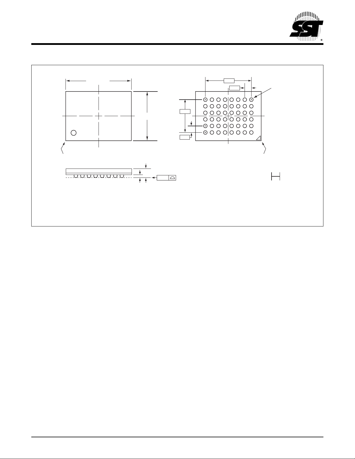
PACKAGING DIAGRAMS
Pin # 1 Identifier
16 Mbit / 32 Mbit / 64 Mbit Multi-Purpose Flash Plus
SST39VF1601 / SST39VF3201 / SST39VF6401
SST39VF1602 / SST39VF3202 / SST39VF6402
1.05
0.95
0.50
BSC
0.27
12.20
11.80
0.17
18.50
18.30
0.70
0.50
Note: 1. Complies with JEDEC publication 95 MO-142 DD dimensions,
although some dimensions may be more stringent.
2. All linear dimensions are in millimeters (max/min).
3. Coplanarity: 0.1 mm
4. Maximum allowable mold flash is 0.15 mm at the package ends, and 0.25 mm between leads.
20.20
19.80
48-LEAD THIN SMALL OUTLINE PACKAGE (TSOP) 12MM X 20MM
SST PACKAGE CODE: EK
0.15
0.05
DETAIL
1.20
max.
0˚- 5˚
0.70
0.50
1mm
48-tsop-EK-8
©2003 Silicon Storage Technology, Inc. S71223-03-000 11/03
30
Page 31
16 Mbit / 32 Mbit / 64 Mbit Multi-Purpose Flash Plus
SST39VF1601 / SST39VF3201 / SST39VF6401
SST39VF1602 / SST39VF3202 / SST39VF6402
8.00 ± 0.20
6
5
4
3
2
1
A B C D E F G H
6.00 ± 0.20
4.00
0.80
H G F E D C B A
Preliminary Specifications
BOTTOM VIEWTOP VIEW
5.60
0.80
0.45 ± 0.05
(48X)
6
5
4
3
2
1
A1 CORNER
SIDE VIEW
SEATING PLANE
Note: 1. Complies with JEDEC Publication 95, MO-210, variant 'AB-1', although some dimensions may be more stringent.
2. All linear dimensions are in millimeters.
3. Coplanarity: 0.12 mm
4. Ball opening size is 0.38 mm (± 0.05 mm)
1.10 ± 0.10
0.12
0.35 ± 0.05
48-BALL THIN-PROFILE, FINE-PITCH BALL GRID ARRAY (TFBGA) 6MM X 8MM
SST PACKAGE CODE: B3K
A1 CORNER
1mm
48-tfbga-B3K-6x8-450mic-4
©2003 Silicon Storage Technology, Inc. S71223-03-000 11/03
31
Page 32

Preliminary Specifications
10.00 ± 0.20
16 Mbit / 32 Mbit / 64 Mbit Multi-Purpose Flash Plus
SST39VF1601 / SST39VF3201 / SST39VF6401
SST39VF1602 / SST39VF3202 / SST39VF6402
BOTTOM VIEWTOP VIEW
5.60
0.80
6
5
4
3
2
1
A B C D E F G H
A1 CORNER
SIDE VIEW
SEATING PLANE
Note: 1. Although many dimensions are similar to those of JEDEC Publication 95, MO-210, this specific package is not registered.
2. All linear dimensions are in millimeters.
3. Coplanarity: 0.12 mm
4. Ball opening size is 0.38 mm (± 0.05 mm)
8.00 ± 0.20
1.10 ± 0.10
0.12
0.35 ± 0.05
4.00
0.80
H G F E D C B A
48-BALL THIN-PROFILE, FINE-PITCH BALL GRID ARRAY (TFBGA) 8MM X 10MM
SST PACKAGE CODE: B1K
6
5
4
3
2
1
0.45 ± 0.05
(48X)
A1 CORNER
1mm
48-tfbga-B1K-8x10-450mic-4
TABLE 18: R
EVISION HISTORY
Number Description Date
00
01
02
03
• Initial release
• Corrected Pin 15 from A20 to NC for SST39VF160x in Figure 1 on page 6
• Changed data sheet title
• 2004 Data Book
Mar 2003
Apr 2003
Jun 2003
Nov 2003
• Updated the B3K and B1K package diagrams
• Added non-Pb MPNs and removed footnote. (See page 28)
Silicon Storage Technolog y, Inc. • 1171 Sonora Court • Sunnyval e , CA 940 86 • Telephone 408-73 5-91 10 • Fax 408-735-9036
www.SuperFlash.com or www.sst.com
©2003 Silicon Storage Technology, Inc. S71223-03-000 11/03
32
 Loading...