

Datasheet SST39VF800A-55-4E-EN, SST39VF800A-55-4E-EK, SST39VF800A-55-4E-B3N, SST39VF800A-55-4E-B3K, SST39VF800A-55-4C-UK Datasheet (Silicon Storage Technology)
...Page 1

©2001 Silicon Storage Technology, Inc.
S71117-04-000 6/01 360
1
The SST logo and SuperFlash are registered trademarks of Silicon Storage Technology, Inc.
MPF is a trademark of Silicon Storage Technology, Inc.
These specifications are subject to change without notice.
Data Sheet
FEATURES:
• Organized as 128K x16 / 256K x16 / 512K x16
• Single Voltage Read and Write Operations
– 3.0-3.6V for SST39LF200A/400A/800A
– 2.7-3.6V for SST39VF200A/400A/800A
• Superior Reliability
– Endurance: 100,000 Cycles (typical)
– Greater than 100 years Data Retention
• Low Power Consumption
– Ac ti ve Current: 20 mA (typical)
– Standby Current: 3 µA (typical)
• Sector-Erase Capability
– Uniform 2 KWord sectors
• Block-Erase Capability
– Uniform 32 KWord blocks
• Fast Read Access Time
– 45 and 55 ns for SST39LF200A /400 A
– 55 ns for SST39LF800A
– 70 and 90 ns for SST39VF200A /40 0A /800 A
• Latched Address and Data
• Fast Erase and Word-Program
– Sector-Erase Time: 18 ms (typical)
– Block-Erase Time: 18 ms (typical)
– Chip-Erase Time: 70 ms (typical)
– Word-Program Time: 14 µs (typical)
– Chip Rewrite Time:
2 seconds (typical) for SST39LF/VF200A
4 seconds (typical) for SST39LF/VF400A
8 seconds (typical) for SST39LF/VF800A
• Automatic Write Timing
– Internal V
PP
Generation
• End-of-Write Detection
– Toggle Bit
– Data# Polling
• CMOS I/O Compatibility
• JEDEC Standard
– Flash EEPROM Pinouts and command sets
• Packages Available
– 48-lead TSOP (12mm x 20mm)
– 48-ball TFBGA (6mm x 8mm)
PRODUCT DESCRIPTION
The SST39LF200A/400A/800A and SST39VF200A/400A/
800A devices are 128K x16 / 256K x16 / 512K x16 CMOS
Multi-Pur pose Flash (M PF) manufactured with S ST’s proprietar y, high performance CMOS Super Flash te chnology.
The split-gate c el l d es ig n a nd thick oxide tunneling in je ct or
attain better reliability and manufacturability compared with
alternate approaches. The SST39LF200A/400A/800A
write (Program or Erase) with a 3.0-3.6V power supply. The
SST39VF200A/400A/800A write (Program or Erase) with a
2.7-3.6V power supply. These devices conform to JEDEC
standard pinouts for x16 memories.
Featuring high performance Word-Program, the
SST39LF200A/400A/800A and SST39VF200A/400A/
800A devices provide a typical Word-Program time of 14
µsec. The devices use T oggle Bit or Data# Polling to detect
the completion of the Pr ogram or Erase o perati on. To protect against inadvertent write, they have on-chip hardware
and software data protect ion schemes. Designed, manufactured, and tested for a wide spectrum of applications,
these devices are offered with a guaran teed enduranc e of
10,000 cycles. Data ret ention is rated at greater than 100
years.
The SST39LF200A/400A/800A and SST39VF200A/400A/
800A devices are suited for applications that require convenient and economic al updating of program, confi guration,
or data memory. For all system applications, they signifi-
cantly improve performanc e and reliability, while lowering
power consumption. Th ey inherently use less e nergy during Erase and Program than alternative flash technologies.
When programming a flash device, the total energy consumed is a function of the applied voltage, current, and
time of application. Since for any given voltage range, the
SuperFlash techn ology uses less current to pr ogram and
has a shorter erase time, the total energy consumed during
any Erase or Program operation is less than alternative
flash technologies. These devices also improve flexibility
while lowering the cost for program, data, and configuration
storage applications.
The SuperFlash te ch no logy pr ovid es fi xed Erase an d P r ogram times, independent o f the num be r of Erase/ Pro gram
cycles that have occurred. Therefore the system software
or hardware does not have to be modified or de-rated as is
necessary with alternative flash technologies, whose Erase
and Program times inc rease with accumul ated Erase/P rogram cycles .
To meet s urface mount requireme nts, the SST39LF20 0A/
400A/800A and SST39 VF200A/400A/800 A are offered in
both 48-lead TSOP packages and 48-ball TFBGA packages. See Figures 1 and 2 for pinouts.
2 Mbit / 4 Mbit / 8 Mbit (x16) Multi-Purpose Flash
SST39LF200A / SST39LF400A / SST39LF800A
SST39VF200A / SST39VF400A / SS T39VF800A
SST39LF/VF200A / 400A / 800A3.0 & 2.7V 2Mb / 4Mb / 8Mb (x16) MPF memories
Page 2

2
Data Sheet
2 Mbit / 4 Mbit / 8 Mbit Multi-Purpose Flash
SST39LF200A / SST39LF400A / SST39LF800A
SST39VF200A / SST39VF400A / SST39VF800A
©2001 Silicon Storage Technology, Inc. S71117-04-000 6/01 360
Device Operation
Commands are used to initiate the memory operation functions of the device. Commands ar e written to the device
using standard mi croprocessor write sequen ces. A command is written by asse r ting WE# low whil e keeping CE#
low. The address bus is latched on the falling edge of WE#
or CE#, whichever occurs last. T he data bus is latche d on
the rising edge of WE# or CE#, whichever occurs first.
Read
The Read oper at io n of th e SST 3 9LF 2 00 A/ 400 A /80 0 A and
SST39VF200A/400A/800A is controlled by CE# and OE#,
both have to be low for the system to obtain data from the
outputs. CE# is use d for device selection. W hen CE# is
high, the chip is deselected and only standby power is consumed. OE# is the out put co ntr o l a nd i s used to gate data
from the output p ins. The data bus is in hi gh impedance
state when either CE# or OE# is high. Refer to the Rea d
cycle timing diagram for further details (Figure 3).
Word-Program Operation
The SST39LF200A/400A/800A and SST39VF200A/400A/
800A are programmed on a word-by-word basis. Before
programming, one must ens ure that the sector, in which
the word which is being programmed exists, is fully erased.
The Program operation consists of three steps. The f irst
step is the three-byte load sequence for Software Data Protection. The second step is to load word address and word
data. During the Word-Program operation, the addres ses
are latched on the falling edge of either CE# or WE#,
whichever occurs last. The data is latched on the rising
edge of either CE# or WE#, whichever occurs first. The
third step is the internal Program operatio n which is initiated after the rising edge of the fourth WE# or CE#, whichever occurs first. The Program operation, once initiated, will
be completed with in 20 µs. See Figures 4 and 5 for WE #
and CE# controlled Program operation timing diagrams
and Figure 16 for flowchar ts. During the Program ope ration, the only valid reads are Dat a# Polling and Toggle Bit.
During the inte rnal Program operat ion, the host is fre e to
perform additional tasks. Any commands issued during the
internal Program operation are ignored.
Sector/Block-Erase Operation
The Sector- (or Block-) Erase operation allows the system
to erase the device on a sector-by-sector (or block-byblock) basis. The SST39LF200A/400A/800A and
SST39VF200A/400A/800A offers both Sector-Erase and
Block-Erase mode. The sector architecture is based on
uniform sector size of 2 K Word. The Block-Era se mode is
based on uniform block size of 32 KWord. The Sector-
Erase operation is initiated by executing a six-byte command sequence with Sector-Erase command (30H) and
sector address (SA) in the last bus cycle. The Block-Erase
operation is initiated by executing a six-byte command
sequence with Block-Erase command (50H) and block
address (BA) in the last bus cycle. The sector or block
address is latched on the falling edge of the sixth WE#
pulse, while the comm and (30H or 50H) is latched on th e
rising edge of the sixth WE# pulse. The internal Erase
operation begins a fter the sixth WE# pulse. The End -ofErase operation can be determined using either Data#
Polling or Toggle Bit methods. See Figures 9 and 10 for timing waveforms. Any commands issued d uring the Sectoror Block-Erase operation are ignored.
Chip-Erase Operation
The SST39LF200A/400A/800A and SST39VF200A/400A/
800A provide a Chip-Erase operation, which allows the
user to erase the entire memory array to the “1” state . Thi s
is useful when t he entir e de vice must be quic kly era sed.
The Chip-Erase operation is initiated by executing a sixbyte command sequence with Chip-Erase command (10H)
at address 5555H in the last byte sequence. The Eras e
operation begins with the rising edge of the sixt h WE# or
CE#, whichever occurs first. During the Erase operation,
the only valid read is T oggle Bit or Data# Polling. See Table
4 for the command sequence, Figure 8 for timing diagram,
and Figure 19 for the flowchart. Any commands issued during the Chip-Erase operation are ignored.
Write Operation Status Detection
The SST39LF200A/400A/800A and SST39VF200A/400A/
800A provi d e tw o sof tw ar e me ans t o det ect t he comp leti on
of a write (Program or Erase) cycle, in order to optimize the
system write cycle time. The software detection includes
two status bits: Data# Polling (DQ
7
) and Toggle Bit (DQ6).
The End-of- Write detecti on mode is enab led afte r the rising
edge of WE#, which initiates the internal Program or Erase
operation.
The actual comple tion of the nonvolatile wr ite is as ynchr onous with the system ; therefore, either a Data# Polling or
Toggle Bit read may be simultan eous with the c ompletion
of the write cycle. If this occurs, the system may possibly
get an erroneous result, i.e., valid data may appear to conflict with either DQ
7
or DQ6. In order to prevent spurious
rejection, if an erroneous result occurs, the software routine
should include a loop to read the accessed location an
additional two (2) times. If bo th reads are valid, then the
device has completed the write cycle, otherwise the rejection is valid.
Page 3

Data Sheet
2 Mbit / 4 Mbit / 8 Mbit Multi-Purpose Flash
SST39LF200A / SST39LF400A / SST39LF800A
SST39VF200A / SST39VF400A / SST39VF800A
3
©2001 Silicon Storage Technology, Inc. S71117-04-000 6/01 360
Data# Polling (DQ7)
When the SST39LF200A/400A/800A and SST39VF200A/
400A/800A are in the internal Program operation, any
attempt to read DQ
7
will produce the complement of the
true data. Onc e the Pr ogram operati on is c ompl eted, D Q
7
will produce true data. The device is then ready for the next
operation. Duri ng inter nal Eras e operation, any attempt t o
read DQ
7
will produce a ‘0’. Once the internal Erase opera-
tion is completed, DQ
7
will produce a ‘1’. The Data# Polling
is valid after the r ising edg e of four th WE# (or CE#) p ulse
for Program operation. For Sector-, Block- or Chip- Erase,
the Data# Polling is valid after the rising edge of sixth WE#
(or CE#) pulse. See Fi gure 6 for Data# Polling timing diagram and F igur e 17 f or a flo wcha rt.
Toggle Bit (DQ6)
During the inter nal Program or Erase ope ration, any consecutive attempts to read DQ
6
will produce alter nating 1s
and 0s, i.e., toggling between 1 and 0. W hen the internal
Program or Erase operat ion is c omplete d, the DQ
6
bit will
stop toggling. The device is the n re ady for the next ope ration. The Toggle Bit is valid after the rising edge of fourth
WE# (or CE#) pulse for Program operat ion. For Sector-,
Block- or Chip-Erase, the Toggle Bit is valid after the rising
edge of sixth WE# (or CE#) pulse. See Figure 7 for Toggle
Bit timing diag ram and Figu re 17 f or a fl owc hart.
Data Protection
The SST39LF200A/400A/800A and SST39VF200A/400A/
800A provide both hardware and software features to protect nonvolatile data from inadvertent writes.
Hardware Data Protection
Noise/Glitch Protection: A WE# or CE# pulse of le ss than 5
ns will not init iate a write cycle .
V
DD
Power Up/Down Detection: The Write operation is
inhibited when V
DD
is less than 1.5V.
Write Inhibit Mode
: Forcing OE# low, CE# high, or WE#
high will inhibit the W r it e operation. This prevents inadvertent writes during p owe r-up o r pow er- down.
Software Data Protection (SDP)
The SST39LF200A/400A/800A and SST39VF200A/400A/
800A provide the JEDEC approved Software Data Protection scheme for all data alteration operations, i.e., Program
and Erase. Any Program operation requires the inclusion of
the three-byte sequen ce. The thr ee-byte l oad se quenc e is
used to initiate the Program operation, providing optimal
protection from inadver tent Write operations, e.g., during
the system power-up or power-down. Any Erase operation
requires the inclus ion of six-byte sequence. Thi s group of
devices are shipped with the Software Data Protection permanently enabled. See Table 4 for the specific software
command codes. During SDP command sequence, invalid
commands will abort the device to Read mode within TRC.
The contents of DQ
15
-DQ8 can be VIL or VIH, but no other
value, during any SDP command sequence.
Common Flash Memory Interface (CFI)
The SST39LF200A/400A/800A and SST39VF200A/400A/
800A also contain the CFI information to describe the characteristics of th e device. In order to enter the CFI Query
mode, the system must writ e three-byte sequence, same
as Software ID Entry command with 98H (CFI Query command) to address 5555H in the last byte sequence. Once
the device enters the CFI Query mode, the system can
read CFI data at the addresses given in Tab les 5 through 9.
The system must wri te th e CFI E xit c omman d to retur n to
Read mode fr om the CFI Query mode .
Page 4

4
Data Sheet
2 Mbit / 4 Mbit / 8 Mbit Multi-Purpose Flash
SST39LF200A / SST39LF400A / SST39LF800A
SST39VF200A / SST39VF400A / SST39VF800A
©2001 Silicon Storage Technology, Inc. S71117-04-000 6/01 360
Product Identification
The Product Id entification mode ide ntifies the devices as
the SST39LF/VF2 00A, SST39LF/VF400A and SST39LF/
VF800A and manufacturer as SST. This mode may be
accessed by software operations. Users may use the
Software Product Identification operation to identify the part
(i.e., using the device ID) when using multiple
manufacturers in the same socket. For details, see Table 4
for software operation, Fi gure 11 for the Software ID En try
and Read timing d iagram, and Fi gure 18 for the So ftware
ID Entry command sequence flowchart.
Product Identification Mode Exit/
CFI Mode Exit
In order to return to the standard Read mode, the Software
Product Identifica tion mode must be exited. Exi t is acco mplished by issuing the Software ID Exit command
sequence, which returns the device to the Read mode.
This command may also be used to reset the device to the
Read mode after any inadvertent transient condition that
apparently causes the device to behave abnorma lly, e.g.,
not read correctly. Please note that the Soft ware ID Exit/
CFI Exit command is ignored during an internal Program or
Erase operation. See Table 4 for software command
codes, Figure 13 for timing waveform and Figure 18 for a
flowchart.
TABLE 1: P
RODUCT IDENTIFICATION TABLE
Address Data
Manufacturer’s ID 0000H 00BFH
Device ID
SST39LF/VF200A 0001H 2789H
SST39LF/VF400A 0001H 2780H
SST39LF/VF800A 0001H 2781H
T1.3 360
Page 5
Data Sheet
2 Mbit / 4 Mbit / 8 Mbit Multi-Purpose Flash
SST39LF200A / SST39LF400A / SST39LF800A
SST39VF200A / SST39VF400A / SST39VF800A
5
©2001 Silicon Storage Technology, Inc. S71117-04-000 6/01 360
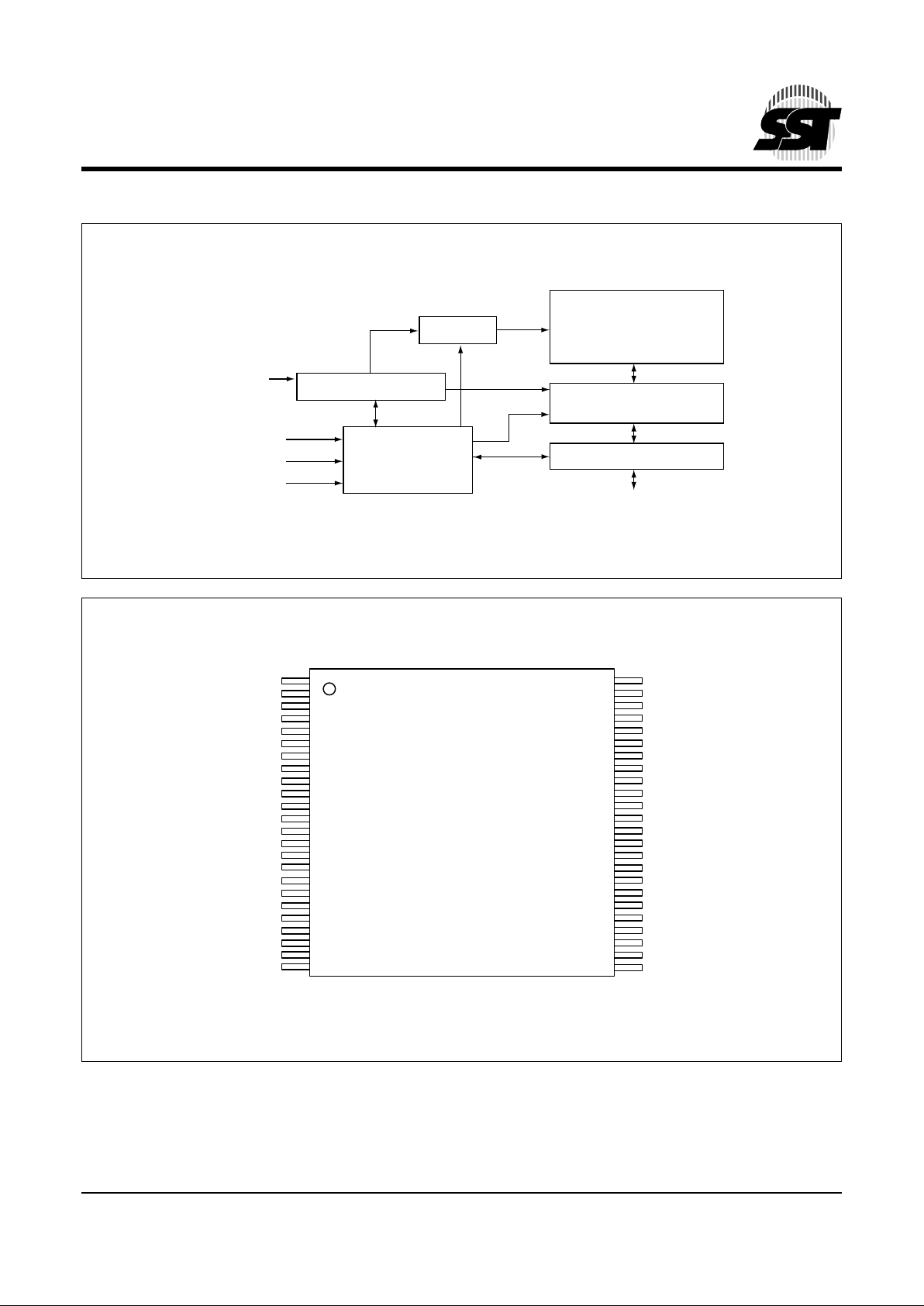
FIGURE 1: PIN ASSIGNMENTS FOR 48-LEAD TSOP
Y-Decoder
I/O Buffers and Data Latches
360 ILL B1.2
Address Buffer & Latches
X-Decoder
DQ15 - DQ
0
Memory Address
OE#
CE#
WE#
SuperFlash
Memory
Control Logic
FUNCTIONAL BLOCK DIAGRAM
A15
A14
A13
A12
A11
A10
A9
A8
NC
NC
WE#
NC
NC
NC
NC
NC
NC
A7
A6
A5
A4
A3
A2
A1
1
2
3
4
5
6
7
8
9
10
11
12
13
14
15
16
17
18
19
20
21
22
23
24
A16
NC
V
SS
DQ15
DQ7
DQ14
DQ6
DQ13
DQ5
DQ12
DQ4
V
DD
DQ11
DQ3
DQ10
DQ2
DQ9
DQ1
DQ8
DQ0
OE#
V
SS
CE#
A0
48
47
46
45
44
43
42
41
40
39
38
37
36
35
34
33
32
31
30
29
28
27
26
25
360 ILL F01.2
Standard Pinout
T op Vie w
Die Up
SST39LF200A/400A/800A
SST39VF200A/400A/800A
SST39LF/VF200A
A15
A14
A13
A12
A11
A10
A9
A8
NC
NC
WE#
NC
NC
NC
NC
NC
A17
A7
A6
A5
A4
A3
A2
A1
SST39LF/VF400A
A15
A14
A13
A12
A11
A10
A9
A8
NC
NC
WE#
NC
NC
NC
NC
A18
A17
A7
A6
A5
A4
A3
A2
A1
SST39LF/VF800A SST39LF/VF200A
A16
NC
V
SS
DQ15
DQ7
DQ14
DQ6
DQ13
DQ5
DQ12
DQ4
V
DD
DQ11
DQ3
DQ10
DQ2
DQ9
DQ1
DQ8
DQ0
OE#
V
SS
CE#
A0
SST39LF/VF400A
A16
NC
V
SS
DQ15
DQ7
DQ14
DQ6
DQ13
DQ5
DQ12
DQ4
V
DD
DQ11
DQ3
DQ10
DQ2
DQ9
DQ1
DQ8
DQ0
OE#
V
SS
CE#
A0
SST39LF/VF800A
Page 6
6
Data Sheet
2 Mbit / 4 Mbit / 8 Mbit Multi-Purpose Flash
SST39LF200A / SST39LF400A / SST39LF800A
SST39VF200A / SST39VF400A / SST39VF800A
©2001 Silicon Storage Technology, Inc. S71117-04-000 6/01 360
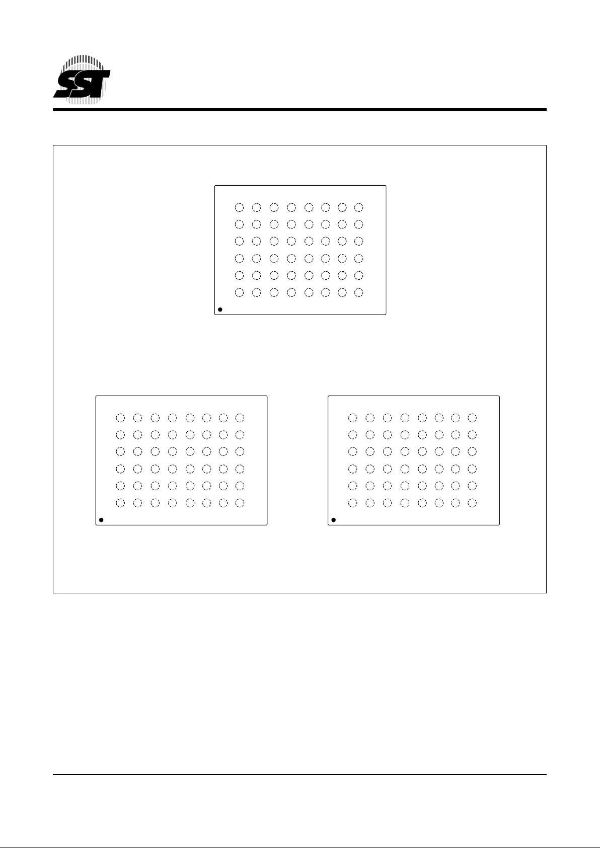
FIGURE 2: PIN ASSIGNMENTS FOR 48-BALL TFBGA
A13
A9
WE#
NC
A7
A3
A12
A8
NC
NC
NC
A4
A14
A10
NC
NC
A6
A2
A15
A11
NC
NC
A5
A1
A16
DQ7
DQ5
DQ2
DQ0
A0
NC
DQ14
DQ12
DQ10
DQ8
CE#
DQ15
DQ13
V
DD
DQ11
DQ9
OE#
V
SS
DQ6
DQ4
DQ3
DQ1
V
SS
360 ILL F02_2.0
SST39LF/VF200A
TOP VIEW (balls facing down)
6
5
4
3
2
1
A B C D E F G H
A13
A9
WE#
NC
A7
A3
A12
A8
NC
NC
A17
A4
A14
A10
NC
NC
A6
A2
A15
A11
NC
NC
A5
A1
A16
DQ7
DQ5
DQ2
DQ0
A0
NC
DQ14
DQ12
DQ10
DQ8
CE#
DQ15
DQ13
V
DD
DQ11
DQ9
OE#
V
SS
DQ6
DQ4
DQ3
DQ1
V
SS
360 ILL F02_4.0
SST39LF/VF400A
TOP VIEW (balls facing down)
6
5
4
3
2
1
A B C D E F G H
A13
A9
WE#
NC
A7
A3
A12
A8
NC
NC
A17
A4
A14
A10
NC
A18
A6
A2
A15
A11
NC
NC
A5
A1
A16
DQ7
DQ5
DQ2
DQ0
A0
NC
DQ14
DQ12
DQ10
DQ8
CE#
DQ15
DQ13
V
DD
DQ11
DQ9
OE#
V
SS
DQ6
DQ4
DQ3
DQ1
V
SS
360 ILL F02_8.0
SST39LF/VF800A
TOP VIEW (balls facing down)
6
5
4
3
2
1
A B C D E F G H
Page 7
Data Sheet
2 Mbit / 4 Mbit / 8 Mbit Multi-Purpose Flash
SST39LF200A / SST39LF400A / SST39LF800A
SST39VF200A / SST39VF400A / SST39VF800A
7
©2001 Silicon Storage Technology, Inc. S71117-04-000 6/01 360
TABLE 2: PIN DESCRIPTION
Symbol Pin Name Functions
A
MS
1
-A
0
Address Inputs To provide memory addresses. During Sector-Erase AMS-A11 address lines w ill s ele ct the
sector. During Block-Erase A
MS-A15
address lines will select the block.
DQ
15
-DQ
0
Data Input/output To output data during Read cycles and receive input data during Write cycles.
Data is internally latched during a Write cycle.
The outputs are in tri-state when OE# or CE# is high.
CE# Chip Enable To activate the device when CE# is low.
OE# Output Enable To gate the data output buffers.
WE# Write Enable To control the Write operations.
V
DD
Power Supply To provide power supply voltage: 3.0-3.6V for SST39LF200A/400A/800A
2.7-3.6V for SST39VF200A/400A/ 800 A
V
SS
Ground
NC No Connection Unconnected pins.
T2.2 360
1. AMS = Most significant address
A
MS
= A16 for SST39LF/VF200A, A17 for SST39LF/VF400A, and A18 for SST39LF/VF800A
TABLE 3: OPERATION MODES SELECTION
Mode CE# OE# WE# DQ Address
Read V
IL
V
IL
V
IH
D
OUT
A
IN
Program V
IL
V
IH
V
IL
D
IN
A
IN
Erase V
IL
V
IH
V
IL
X
1
1. X can be VIL or VIH, but no other value.
Sector or Block address,
XXH for Chip-Erase
Standby V
IH
XXHigh Z X
Write Inhibit X V
IL
XHigh Z/ D
OUT
X
XXV
IH
High Z/ D
OUT
X
Product Identification
Software Mode V
IL
V
IL
V
IH
See Table 4
T3.4 360
Page 8
8
Data Sheet
2 Mbit / 4 Mbit / 8 Mbit Multi-Purpose Flash
SST39LF200A / SST39LF400A / SST39LF800A
SST39VF200A / SST39VF400A / SST39VF800A
©2001 Silicon Storage Technology, Inc. S71117-04-000 6/01 360
TABLE 4: SOFTWARE COMMAND SEQUENCE
Command
Sequence
1st Bus
Write Cycle
2nd Bus
Write Cycle
3rd Bus
Write Cycle
4th Bus
Write Cycle
5th Bus
Write Cycle
6th Bus
Write Cycle
Addr1Data2Addr1Data2Addr1Data2Addr1Data2Addr1Data2Addr1Data
2
Word-Program 5555H AAH 2AAAH 55H 5555H A0H WA3Data
Sector-Erase 5555H AAH 2AAAH 55H 5555H 80H 5555H AAH 2AAAH 55H SA
X
4
30H
Block-Erase 5555H AAH 2AAAH 55H 5555H 80H 5555H AAH 2AAAH 55H BA
X
4
50H
Chip-Erase 5555H AAH 2AAAH 55H 5555H 80H 5555H AAH 2AAAH 55H 5555H 10H
Software ID Entry
5,6
5555H AAH 2AAAH 55H 5555H 90H
CFI Query Entry
5
5555H AAH 2AAAH 55H 5555H 98H
Software ID Exit
7
/
CFI Exit
XXH F0H
Software ID Exit
7
/
CFI Exit
5555H AAH 2AAAH 55H 5555H F0H
T4.2 360
1. Addres s format A14-A0 (Hex),
Addresses A
15
and A16 can be VIL or VIH, but no other value, for the Command sequence for SST39LF/VF200A.
Addresses A
15
, A16, and A17 can be VIL or VIH, but no other value, for the Command sequence for SST39LF/VF400A.
Addresses A
15
, A16, A17, and A18 can be VIL or VIH, but no other value, for the Command sequence for SST39LF/VF800A.
2. DQ
15
- DQ8 can be VIL or VIH, but no other value, for the Command sequence
3. WA = Program word address
4. SA
X
for Sector-Erase; uses AMS-A11 address lines
BA
X
, for Block-Erase; uses AMS-A15 address lines
A
MS
= Most significant address
A
MS
= A16 for SST39LF/VF200A, A17 for SST39LF/VF400A and A18 for SST39LF/VF800A
5. The device does not remain in Software Product ID Mode if powered down.
6. With A
MS-A1
=0; SST Manufacturer’s ID= 00BFH, is read with A0 = 0,
SST39LF/VF200A Device ID = 2789H, is read with A
0
= 1.
SST39LF/VF400A Device ID = 2780H, is read with A
0
= 1.
SST39LF/VF800A Device ID = 2781H, is read with A
0
= 1.
7. Both Software ID Exit operations are equivalent
TABLE 5: CFI QUERY IDENTIFICATION STRING1 FOR SST39LF200A/400A/800A AND SST39VF200A/400A/800A
1. Refer to CFI publication 100 for more details.
Address Data Data
10H 0051H Query Unique ASCII string “QRY”
11H 0052H
12H 0059H
13H 0001H Primary OEM command set
14H 0007H
15H 0000H Address for Primary Extended Table
16H 0000H
17H 0000H Alternate OEM command set (00H = none exists)
18H 0000H
19H 0000H Address for Alternate OEM extended Table (00H = none exits)
1AH 0000H
T5.0 360
Page 9
Data Sheet
2 Mbit / 4 Mbit / 8 Mbit Multi-Purpose Flash
SST39LF200A / SST39LF400A / SST39LF800A
SST39VF200A / SST39VF400A / SST39VF800A
9
©2001 Silicon Storage Technology, Inc. S71117-04-000 6/01 360
TABLE 6: SYSTEM INTERFACE INFORMATION FOR SST39LF200 A/400A/800A AND S ST39VF200A/4 00A/800A
Address Data Data
1BH 0027H
1
VDD Min. (Program/Erase)
0030H1DQ7-DQ4: Volts, DQ3-DQ0: 100 millivolts
1CH 0036H V
DD
Max. (Program/Erase)
DQ
7
-DQ4: Volts, DQ3-DQ0: 100 millivolts
1DH 0000H V
PP
min. (00H = no VPP pin)
1EH 0000H V
PP
max. (00H = no VPP pin)
1FH 0004H Typical time out for Word-Progra m 2
N
µs (24 = 16 µs)
20H 0000H Typical time out for min. size buffer program 2
N
µs (00H = not supported)
21H 0004H Typical time out for indiv idu al Sec tor/Bl ock-Erase 2
N
ms (24 = 16 ms)
22H 0006H Typical time out for Chip -Erase 2
N
ms (26 = 64 ms)
23H 0001H Maximum time out for Word-Program 2N times typical (21 x 24 = 32 µs)
24H 0000H Maximum time out for buffer program 2N times typical
25H 0001H Maximum time out for individual Sector/Block-Erase 2
N
times typical (21 x 24 = 32 ms)
26H 0001H Maximum time out for Chip-Erase 2N times typical (21 x 26 = 128 ms)
T6.2 360
1. 0030H for SST39LF200A/400A/800A and 0027H for SST39VF200A/400A/800A
TABLE 7: DEVICE GEOMETRY INFORMATION FOR SST39LF/VF200A
Address Data Data
27H 0012H Device size = 2
N
Byte (12H = 18; 218 = 256 KBytes)
28H 0001H Flash Device Interface description; 0001H = x16-only asynchronous interface
29H 0000H
2AH 0000H Maximum number of byte in multi-byte write = 2
N
(00H = not supported)
2BH
2CH 0002H Number of Erase Sector/Block sizes supported by device
2DH 003FH Sector Information (y + 1 = Number of sectors; z x 256B = sector size)
2EH 0000H y = 63 + 1 = 64 sectors (003FH = 63)
2FH 0010H
30H 0000H z = 16 x 256 Bytes = 4 KBytes/sector (0010H = 16)
31H 0003H Block Information (y + 1 = Number of blocks; z x 256B = block size)
32H 0000H y = 3 + 1 = 4 blocks (0003H = 3)
33H 0000H
34H 0001H z = 256 x 256 Bytes = 64 KBytes/block (0100H = 256)
T7.2 360
Page 10

10
Data Sheet
2 Mbit / 4 Mbit / 8 Mbit Multi-Purpose Flash
SST39LF200A / SST39LF400A / SST39LF800A
SST39VF200A / SST39VF400A / SST39VF800A
©2001 Silicon Storage Technology, Inc. S71117-04-000 6/01 360
TABLE 8: DEVICE GEOMETRY INFORMATION FOR SST39LF/VF400A
Address Data Data
27H 0013H Device size = 2
N
Byte (13H = 19; 219 = 512 KBytes)
28H 0001H Flash Device Interface description; 0001H = x16-only asynchronous interface
29H 0000H
2AH 0000H Maximum number of byte in multi-byte write = 2
N
(00H = not supported)
2BH 0000H
2CH 0002H Number of Erase Sector/Block sizes supported by device
2DH 007FH Sector Information (y + 1 = Number of sectors; z x 256B = sector size)
2EH 0000H y = 127 + 1 = 128 sectors (007FH = 127)
2FH 0010H
30H 0000H z = 16 x 256 Bytes = 4 KBytes/sector (0010H = 16)
31H 0007H Block Information (y + 1 = Number of blocks; z x 256B = block size)
32H 0000H y = 7 + 1 = 8 blocks (0007H = 7)
33H 0000H
34H 0001H z = 256 x 256 Bytes = 64 KBytes/block (0100H = 256)
T8.1 360
TABLE 9: DEVICE GEOMETRY INFORMATION FOR SST39LF/VF800A
Address Data Data
27H 0014H Device size = 2
N
Byte (14H = 20; 220 = 1 MByte)
28H 0001H Flash Device Interface description; 0001H = x16-only asynchronous interface
29H 0000H
2AH 0000H Maximum number of byte in multi-byte write = 2
N
(00H = not supported)
2BH 0000H
2CH 0002H Number of Erase Sector/Block sizes supported by device
2DH 00FFH Sector Information (y + 1 = Number of sectors; z x 256B = sector size)
2EH 0000H y = 255 + 1 = 256 sectors (00FFH = 255)
2FH 0010H
30H 0000H z = 16 x 256 Bytes = 4 KBytes/sector (0010H = 16)
31H 000FH Block Information (y + 1 = Number of blocks; z x 256B = block size)
32H 0000H y = 15 + 1 = 16 blocks (000FH = 15)
33H 0000H
34H 0001H z = 256 x 256 Bytes = 64 KBytes/block (0100H = 256)
T9.0 360
Page 11

Data Sheet
2 Mbit / 4 Mbit / 8 Mbit Multi-Purpose Flash
SST39LF200A / SST39LF400A / SST39LF800A
SST39VF200A / SST39VF400A / SST39VF800A
11
©2001 Silicon Storage Technology, Inc. S71117-04-000 6/01 360
Absolute Maximum Stress Ratings (Applied conditions greater than those listed under “Absolute Maximum
Stress Ratings” may cause pe r manent dama ge to the device. This is a stres s rating only and funct ional operatio n
of the device at these conditions or conditions greater tha n those defined in the ope rational sections of this data
sheet is not implied. Exposure to absolute maximum stress rating conditions may affect device reliability.)
Temperature Under Bias . . . . . . . . . . . . . . . . . . . . . . . . . . . . . . . . . . . . . . . . . . . . . . . . . . . . . . . . . -55°C to +125°C
Storage Temperature . . . . . . . . . . . . . . . . . . . . . . . . . . . . . . . . . . . . . . . . . . . . . . . . . . . . . . . . . . . -65°C to +150°C
D. C. Voltage on Any Pin to Ground Potential . . . . . . . . . . . . . . . . . . . . . . . . . . . . . . . . . . . . . . .-0.5V to V
DD
+ 0.5V
Transient Voltage (<20 ns) on Any Pin to Ground Potential . . . . . . . . . . . . . . . . . . . . . . . . . . . .-1.0V to V
DD
+ 1.0V
Voltage on A
9
Pin to Ground Potential . . . . . . . . . . . . . . . . . . . . . . . . . . . . . . . . . . . . . . . . . . . . . . . . -0.5V to 13.2V
Package Power Dissipation Capability (Ta = 25°C) . . . . . . . . . . . . . . . . . . . . . . . . . . . . . . . . . . . . . . . . . . . . . . 1.0W
Surface Mount Lead Soldering Temperature (3 Seconds) . . . . . . . . . . . . . . . . . . . . . . . . . . . . . . . . . . . . . . . 240°C
Output Short Circ uit Curr ent
1
. . . . . . . . . . . . . . . . . . . . . . . . . . . . . . . . . . . . . . . . . . . . . . . . . . . . . . . . . . . . . 50 mA
1. Outputs shorted for no more than one second. No more than one output shorted at a time.
OPERATING RANGE: SST39LF200A/400A/800A
Range Ambient Temp V
DD
Commercial 0°C to +70°C 3.0-3.6V
OPERATING RANGE: SST39VF200A/400A/800A
Range Ambient Temp V
DD
Commercial 0°C to +70°C 2.7-3.6V
Extended -20°C to +85°C 2.7-3.6V
Industrial -40°C to +85°C 2.7-3.6V
AC CONDITIONS OF TEST
Input Rise/Fall Time . . . . . . . . . . . . . . 5 ns
Output Load . . . . . . . . . . . . . . . . . . . . CL = 30 pF for SST39LF200A/400A/800A
Output Load . . . . . . . . . . . . . . . . . . . . C
L
= 100 pF for SST39VF200A/400A/800A
See Figures 14 and 15
Page 12

12
Data Sheet
2 Mbit / 4 Mbit / 8 Mbit Multi-Purpose Flash
SST39LF200A / SST39LF400A / SST39LF800A
SST39VF200A / SST39VF400A / SST39VF800A
©2001 Silicon Storage Technology, Inc. S71117-04-000 6/01 360
TABLE 10: DC OPERATING CHARACTERISTICS
VDD = 3.0-3.6V FOR SST39LF20 0A/400A/800A AND 2.7-3.6V FOR S ST39VF200A/4 00A/800A
Symbol Parameter
Limits
Test ConditionsMin Max Units
I
DD
Power Supply Current Address input = VIL/VIH, at f=1/TRC Min.,
V
DD=VDD
Max.
Read 30 mA CE#=OE#=V
IL
,WE#=VIH, all I/Os open
Program and Erase 30 mA CE#=WE#=V
IL
, OE#=V
IH
I
SB
Standby VDD Current 20 µA CE#=V
IHC
, VDD = VDD Max.
I
LI
Input Leakage Current 1 µA VIN =GND to VDD, VDD = VDD Max.
I
LO
Output Leakage Current 10 µA V
OUT
=GND to VDD, VDD = VDD Max.
V
IL
Input Low Voltage 0.8 VDD = VDD Min.
V
IH
Input High Voltage 0.7V
DD
VVDD = VDD Max.
V
IHC
Input High Voltage (CMOS) VDD-0.3 V VDD = VDD Max.
V
OL
Output Low Voltage 0.2 V IOL = 100 µA, VDD = VDD Min.
V
OH
Output High Voltage VDD-0.2 V IOH = -100 µA, VDD = VDD Min.
T10.5 360
TABLE 11: RECOMMENDED SYSTEM POWER-UP TIMINGS
Symbol Parameter Minimum Units
T
PU-READ
1
1. This parameter is measured only for initial qualification and after a design or process change that could affect this parameter.
Power-up to Read Operation 100 µs
T
PU-WRITE
1
Power-up to Program/Erase Operation 100 µs
T11.0 360
TABLE 12: CAPACITANCE (Ta = 25°C, f=1 Mhz, other pins open)
Parameter Description Test Condition Maximum
C
I/O
1
1. This parameter is measured only for initial qualification and after a design or process change that could affect this parameter.
I/O Pin Capacitance V
I/O
= 0V 12 pF
C
IN
1
Input Capacitance VIN = 0V 6 pF
T12.0 360
TABLE 13: RELIABILITY CHARACTERISTICS
Symbol Parameter Minimum Specification Units Test Method
N
END
1
1. This parameter is measured only for initial qualification and after a design or process change that could affect this parameter.
Endurance 10,000 Cycles JEDEC Standard A117
T
DR
1
Data Retention 100 Years JEDEC Standard A103
I
LTH
1
Latch Up 100 + I
DD
mA JEDEC Standard 78
T13.1 360
Page 13

Data Sheet
2 Mbit / 4 Mbit / 8 Mbit Multi-Purpose Flash
SST39LF200A / SST39LF400A / SST39LF800A
SST39VF200A / SST39VF400A / SST39VF800A
13
©2001 Silicon Storage Technology, Inc. S71117-04-000 6/01 360
AC CHARACTERISTICS
TABLE 14: READ CYCLE TIMIN G PARAMETERS VDD = 3.0-3.6V
Symbol Parameter
SST39LF200A/400A-45 SST39LF200A/400A/800A-55
UnitsMin Max Min Max
T
RC
Read Cycle Time 45 55 ns
T
CE
Chip Enable Access Time 45 55 ns
T
AA
Address Access Time 45 55 ns
T
OE
Output Enable Access Time 30 30 ns
T
CLZ
1
1. This parameter is measured only for initial qualification and after a design or process change that could affect this parameter.
CE# Low to Active Output 0 0 ns
T
OLZ
1
OE# Low to Active Output 0 0 ns
T
CHZ
1
CE# High to High-Z Output 15 15 ns
T
OHZ
1
OE# High to High-Z Output 15 15 ns
T
OH
1
Output Hold from Address Change 0 0 n s
T14.7 360
TABLE 15: READ CYCLE TIMIN G PARAMETERS VDD= 2.7-3.6V
Symbol Parameter
SST39VF200A/400A/800A-70 SST39VF200A/400A/800A-90
UnitsMin Max Min Max
T
RC
Read Cycle Time 70 90 ns
T
CE
Chip Enable Access Time 70 90 ns
T
AA
Address Access Time 70 90 ns
T
OE
Output Enable Access Time 35 45 ns
T
CLZ
1
1. This parameter is measured only for initial qualification and after a design or process change that could affect this parameter.
CE# Low to Active Output 0 0 ns
T
OLZ
1
OE# Low to Active Output 0 0 ns
T
CHZ
1
CE# High to High-Z Output 20 30 ns
T
OHZ
1
OE# High to High-Z Output 20 30 ns
T
OH
1
Output Hold from Address Change 0 0 ns
T15.6 360
Page 14

14
Data Sheet
2 Mbit / 4 Mbit / 8 Mbit Multi-Purpose Flash
SST39LF200A / SST39LF400A / SST39LF800A
SST39VF200A / SST39VF400A / SST39VF800A
©2001 Silicon Storage Technology, Inc. S71117-04-000 6/01 360
TABLE 16: PROGRAM/ERASE CYCLE TIMIN G PARAMETERS
Symbol Parameter Min Max Units
T
BP
Word-Program Time 20 µs
T
AS
Address Setup Time 0 ns
T
AH
Address Hold Time 30 ns
T
CS
WE# and CE# Setup Time 0 ns
T
CH
WE# and CE# Hold Time 0 ns
T
OES
OE# High Setup Time 0 ns
T
OEH
OE# High Hold Time 10 ns
T
CP
CE# Pulse Width 40 ns
T
WP
WE# Pulse Width 40 ns
T
WPH
1
WE# Pulse Width High 30 ns
T
CPH
1
CE# Pulse Width High 30 ns
T
DS
Data Setup Time 30 ns
T
DH
1
Data Hold Time 0 ns
T
IDA
1
Software ID Access and Exit Time 150 ns
T
SE
Sector-Erase 25 ms
T
BE
Block-Erase 25 ms
T
SCE
Chip-Erase 100 ms
T16.0 360
1. This parameter is measured only for initial qualification and after a design or process change that could affect this parameter.
Page 15

Data Sheet
2 Mbit / 4 Mbit / 8 Mbit Multi-Purpose Flash
SST39LF200A / SST39LF400A / SST39LF800A
SST39VF200A / SST39VF400A / SST39VF800A
15
©2001 Silicon Storage Technology, Inc. S71117-04-000 6/01 360
FIGURE 3: READ CYCLE TIMING DIAGRAM
FIGURE 4: WE# CONTROLLED PROGRAM CYCLE TIMING DIAGRAM
360 ILL F03.2
ADDRESS A
MS-0
DQ
15-0
WE#
OE#
CE#
T
CE
T
RC
T
AA
T
OE
T
OLZV
IH
HIGH-Z
T
CLZ
T
OH
T
CHZ
HIGH-Z
DATA VALIDDATA VALID
T
OHZ
Note: AMS = Most significant address
AMS = A16 for SST39LF/VF200A, A17 for SST39LF/VF400A and A18 for SST39LF/VF800A
360 ILL F04.4
ADDRESS A
MS-0
DQ
15-0
T
DH
T
WPH
T
DS
T
WP
T
AH
T
AS
T
CH
T
CS
CE#
SW0 SW1 SW2
5555 2AAA 5555 ADDR
XXAA XX55 XXA0 DATA
INTERNAL PROGRAM OPERATION STARTS
WORD
(ADDR/DATA)
OE#
WE#
T
BP
Note: AMS = Most significant address
AMS = A16 for SST39LF/VF200A, A17 for SST39LF/VF400A and A18 for SST39LF/VF800A
X can be VIL or VIH, but no other value.
Page 16

16
Data Sheet
2 Mbit / 4 Mbit / 8 Mbit Multi-Purpose Flash
SST39LF200A / SST39LF400A / SST39LF800A
SST39VF200A / SST39VF400A / SST39VF800A
©2001 Silicon Storage Technology, Inc. S71117-04-000 6/01 360
FIGURE 5: CE# CONTROLLED PROGRAM CYCLE TIMING DIAGRAM
FIGURE 6: DATA# POLLING TIMING D IAGRAM
360 ILL F05.4
ADDRESS A
MS-0
DQ
15-0
T
DH
T
CPH
T
DS
T
CP
T
AH
T
AS
T
CH
T
CS
WE#
SW0 SW1 SW2
5555 2AAA 5555 ADDR
XXAA XX55 XXA0 DATA
INTERNAL PROGRAM OPERATION STARTS
WORD
(ADDR/DATA)
OE#
CE#
T
BP
Note: AMS = Most significant address
AMS = A16 for SST39LF/VF200A, A17 for SST39LF/VF400A and A18 for SST39LF/VF800A
X can be VIL or VIH, but no other value.
360 ILL F06.3
ADDRESS A
MS-0
DQ
7
DATA DATA# DATA# DATA
WE#
OE#
CE#
T
OEH
T
OE
T
CE
T
OES
Note: AMS = Most significant address
AMS = A16 for SST39LF/VF200A, A17 for SST39LF/VF400A and A18 for SST39LF/VF800A
Page 17

Data Sheet
2 Mbit / 4 Mbit / 8 Mbit Multi-Purpose Flash
SST39LF200A / SST39LF400A / SST39LF800A
SST39VF200A / SST39VF400A / SST39VF800A
17
©2001 Silicon Storage Technology, Inc. S71117-04-000 6/01 360
FIGURE 7: TOGGLE BIT TIMING DIAGRAM
FIGURE 8: WE# CONTROLLED CHIP-ERASE TIMING DIAGRAM
360 ILL F07.3
ADDRESS A
MS-0
DQ
6
WE#
OE#
CE#
T
OET
OEH
T
CE
T
OES
TWO READ CYCLES
WITH SAME OUTPUTS
Note: AMS = Most significant address
AMS = A16 for SST39LF/VF200A, A17 for SST39LF/VF400A and A18 for SST39LF/VF800A
360 ILL F08.7
ADDRESS A
MS-0
DQ
15-0
WE#
SW0 SW1 SW2 SW3 SW4 SW5
5555 2AAA 2AAA5555 5555
XX55 XX10XX55XXAA XX80 XXAA
5555
OE#
CE#
SIX-BYTE CODE FOR CHIP-ERASE
T
SCE
T
WP
Note: This device also supports CE# controlled Chip-Erase operation. The WE# and CE# signals are
interchageable as long as minimum timings are met. (See Table 16)
AMS = Most significant address
AMS = A16 for SST39LF/VF200A, A17 for SST39LF/VF400A and A18 for SST39LF/VF800A
X can be VIL or VIH, but no other value.
Page 18

18
Data Sheet
2 Mbit / 4 Mbit / 8 Mbit Multi-Purpose Flash
SST39LF200A / SST39LF400A / SST39LF800A
SST39VF200A / SST39VF400A / SST39VF800A
©2001 Silicon Storage Technology, Inc. S71117-04-000 6/01 360
FIGURE 9: WE# CONTROLLED BLOCK-ERASE TIMING DIAGRAM
FIGURE 10: WE# CONTROLLED SECTOR-ERASE TIMING DIAGRAM
360 ILL F17.9
ADDRESS A
MS-0
DQ
15-0
WE#
SW0 SW1 SW2 SW3 SW4 SW5
5555 2AAA 2AAA5555 5555
XX55 XX50XX55XXAA XX80 XXAA
BA
X
OE#
CE#
SIX-BYTE CODE FOR BLOCK-ERASE
T
BE
T
WP
Note: This device also supports CE# controlled Block-Erase operation. The WE# and CE# signals are
interchageable as long as minimum timings are met. (See Table 16)
BAX = Block Address
AMS = Most significant address
AMS = A16 for SST39LF/VF200A, A17 for SST39LF/VF400A and A18 for SST39LF/VF800A
X can be VIL or VIH, but no other value.
360 ILL F18.8
ADDRESS A
MS-0
DQ
15-0
WE#
SW0 SW1 SW2 SW3 SW4 SW5
5555 2AAA 2AAA5555 5555
XX55 XX30XX55XXAA XX80 XXAA
SA
X
OE#
CE#
SIX-BYTE CODE FOR SECTOR-ERASE
T
SE
T
WP
Note: This device also supports CE# controlled Sector-Erase operation. The WE# and CE# signals are
interchageable as long as minimum timings are met. (See Table 16)
SAX = Sector Address
AMS = Most significant address
AMS = A16 for SST39LF/VF200A, A17 for SST39LF/VF400A and A18 for SST39LF/VF800A
X can be VIL or VIH, but no other value.
Page 19

Data Sheet
2 Mbit / 4 Mbit / 8 Mbit Multi-Purpose Flash
SST39LF200A / SST39LF400A / SST39LF800A
SST39VF200A / SST39VF400A / SST39VF800A
19
©2001 Silicon Storage Technology, Inc. S71117-04-000 6/01 360
FIGURE 11: SOFTWARE ID ENTRY AND READ
FIGURE 12: CFI QUERY ENTRY AND READ
360 ILL F09.4
ADDRESS A
14-0
T
IDA
DQ
15-0
WE#
SW0
SW1 SW2
5555 2AAA 5555 0000 0001
OE#
CE#
THREE-BYTE SEQUENCE FOR
SOFTWARE ID ENTRY
T
WP
T
WPH
T
AA
00BF
Device ID
XX55XXAA XX90
Device ID = 2789H for SST39LF/VF200A, 2780H for SST39LF/VF400A and 2781H for SST39LF/VF800A
Note: X can be VIL or VIH, but no other value.
360 ILL F20.1
ADDRESS A
14-0
T
IDA
DQ
15-0
WE#
SW0
SW1 SW2
5555 2AAA 5555
OE#
CE#
THREE-BYTE SEQUENCE FOR
CFI QUERY ENTRY
T
WP
T
WPH
T
AA
XX55XXAA XX98
Note: X can be VIL or VIH, but no other value.
Page 20

20
Data Sheet
2 Mbit / 4 Mbit / 8 Mbit Multi-Purpose Flash
SST39LF200A / SST39LF400A / SST39LF800A
SST39VF200A / SST39VF400A / SST39VF800A
©2001 Silicon Storage Technology, Inc. S71117-04-000 6/01 360
FIGURE 13: SOFTWARE ID EXIT/CFI EXIT
360 ILL F10.1
ADDRESS A
14-0
DQ
15-0
T
IDA
T
WP
T
WHP
WE#
SW0 SW1 SW2
5555 2AAA 5555
THREE-BYTE SEQUENCE FOR
SOFTWARE ID EXIT AND RESET
OE#
CE#
XXAA XX55 XXF0
Note: X can be VIL or VIH, but no other value.
Page 21

Data Sheet
2 Mbit / 4 Mbit / 8 Mbit Multi-Purpose Flash
SST39LF200A / SST39LF400A / SST39LF800A
SST39VF200A / SST39VF400A / SST39VF800A
21
©2001 Silicon Storage Technology, Inc. S71117-04-000 6/01 360
FIGURE 14: AC INPUT/OUTPUT REFERENCE WAVEFORMS
FIGURE 15: A TEST LOAD EXAMPLE
360 ILL F11.1
REFERENCE POINTS OUTPUTINPUT
V
IT
V
IHT
V
ILT
V
OT
AC test inputs are driven at V
IHT
(0.9 VDD) for a logic “1” and V
IL T
(0.1 VDD) for a logic “0”. Measurement reference points
for inputs and outputs are V
IT
(0.5 VDD) and VOT (0.5 VDD). Input rise and fall times (10% ↔ 90%) are <5 ns.
Note: V
IT
- V
INPUT
Test
V
OT
- V
OUTPUT
Test
V
IHT
- V
INPUT
HIGH Test
V
ILT
- V
INPUT
LOW Test
360 ILL F12.1
TO TESTER
TO DUT
C
L
Page 22

22
Data Sheet
2 Mbit / 4 Mbit / 8 Mbit Multi-Purpose Flash
SST39LF200A / SST39LF400A / SST39LF800A
SST39VF200A / SST39VF400A / SST39VF800A
©2001 Silicon Storage Technology, Inc. S71117-04-000 6/01 360
FIGURE 16: WORD-PROGRAM ALGORITHM
360 ILL F13.4
Start
Load data: XXAAH
Address: 5555H
Load data: XX55H
Address: 2AAAH
Load data: XXA0H
Address: 5555H
Load Word
Address/Word
Data
Wait for end of
Program (TBP,
Data# Polling
bit, or Toggle bit
operation)
Program
Completed
Note: X can be VIL or VIH, but no other value.
Page 23

Data Sheet
2 Mbit / 4 Mbit / 8 Mbit Multi-Purpose Flash
SST39LF200A / SST39LF400A / SST39LF800A
SST39VF200A / SST39VF400A / SST39VF800A
23
©2001 Silicon Storage Technology, Inc. S71117-04-000 6/01 360
FIGURE 17: WAIT OPTIONS
360 ILL F14.0
Wait TBP,
T
SCE, TSE
or T
BE
Program/Erase
Initiated
Internal Timer
Toggle Bit
Yes
Yes
No
No
Program/Erase
Completed
Does DQ
6
match?
Read same
word
Data# Polling
Program/Erase
Completed
Program/Erase
Completed
Read word
Is DQ7 =
true data?
Read DQ
7
Program/Erase
Initiated
Program/Erase
Initiated
Page 24

24
Data Sheet
2 Mbit / 4 Mbit / 8 Mbit Multi-Purpose Flash
SST39LF200A / SST39LF400A / SST39LF800A
SST39VF200A / SST39VF400A / SST39VF800A
©2001 Silicon Storage Technology, Inc. S71117-04-000 6/01 360
FIGURE 18: SOFTWARE ID/CFI COMMAND FLOWCHARTS
360 ILL F15.4
Load data: XXAAH
Address: 5555H
Software ID Entry
Command Sequence
Load data: XX55H
Address: 2AAAH
Load data: XX90H
Address: 5555H
Wait T
IDA
Read Software ID
Load data: XXAAH
Address: 5555H
CFI Query Entry
Command Sequence
Load data: XX55H
Address: 2AAAH
Load data: XX98H
Address: 5555H
Wait T
IDA
Read CFI data
Load data: XXAAH
Address: 5555H
Software ID Exit/CFI Exit
Command Sequence
Load data: XX55H
Address: 2AAAH
Load data: XXF0H
Address: 5555H
Load data: XXF0H
Address: XXH
Return to normal
operation
Wait T
IDA
Wait T
IDA
Return to normal
operation
Note: X can be VIL or VIH, but no other value.
Page 25

Data Sheet
2 Mbit / 4 Mbit / 8 Mbit Multi-Purpose Flash
SST39LF200A / SST39LF400A / SST39LF800A
SST39VF200A / SST39VF400A / SST39VF800A
25
©2001 Silicon Storage Technology, Inc. S71117-04-000 6/01 360
FIGURE 19: ERASE COMMAND SEQUENCE
360 ILL F16.5
Load data: XXAAH
Address: 5555H
Chip-Erase
Command Sequence
Load data: XX55H
Address: 2AAAH
Load data: XX80H
Address: 5555H
Load data: XX55H
Address: 2AAAH
Load data: XX10H
Address: 5555H
Load data: XXAAH
Address: 5555H
Wait T
SCE
Chip erased
to FFFFH
Load data: XXAAH
Address: 5555H
Sector-Erase
Command Sequence
Load data: XX55H
Address: 2AAAH
Load data: XX80H
Address: 5555H
Load data: XX55H
Address: 2AAAH
Load data: XX30H
Address: SA
X
Load data: XXAAH
Address: 5555H
Wait T
SE
Sector erased
to FFFFH
Load data: XXAAH
Address: 5555H
Block-Erase
Command Sequence
Load data: XX55H
Address: 2AAAH
Load data: XX80H
Address: 5555H
Load data: XX55H
Address: 2AAAH
Load data: XX50H
Address: BA
X
Load data: XXAAH
Address: 5555H
Wait T
BE
Block erased
to FFFFH
Note: X can be VIL or VIH, but no other value.
Page 26

26
Data Sheet
2 Mbit / 4 Mbit / 8 Mbit Multi-Purpose Flash
SST39LF200A / SST39LF400A / SST39LF800A
SST39VF200A / SST39VF400A / SST39VF800A
©2001 Silicon Storage Technology, Inc. S71117-04-000 6/01 360
PRODUCT ORDERING INFORMATION
Device Speed Suffix1 Suffix2
SST39x
FxxxA- XX -XX -XX
Package Modifier
K = 48 leads or balls
Numeric = Die modifier
Package Type
E = TSOP (12mm x 20mm)
B3 = TFBGA (0.8mm pitch, 6mm x 8mm)
U = Unencapsulated die
Temperature Range
C = Commercial = 0°C to +70°C
E = Extended = -20°C to +85°C
I = Industrial = -40°C to +85°C
Minimum Endurance
4 = 10,000 cycles
Read Access Speed
45 = 45 ns
55 = 55 ns
70 = 70 ns
90 = 90 ns
Device Density
200 = 2 Megabit
400 = 4 Megabit
800 = 8 Megabit
Voltage
L = 3.0-3.6V
V = 2.7-3.6V
Page 27

Data Sheet
2 Mbit / 4 Mbit / 8 Mbit Multi-Purpose Flash
SST39LF200A / SST39LF400A / SST39LF800A
SST39VF200A / SST39VF400A / SST39VF800A
27
©2001 Silicon Storage Technology, Inc. S71117-04-000 6/01 360
Valid combinations for SST39LF200A
SST39LF200A-45-4C-EK S ST39LF200A-45-4C-B3K
SST39LF200A-55-4C-EK S ST39LF200A-55-4C-B3K
Valid combinations for SST39VF200A
SST39VF200A-70-4C-EK SST39VF200A-70-4C-B3K
SST39VF200A-90-4C-EK SST39VF200A-90-4C-B3K
SST39VF200A-90-4C-U1
SST39VF200A-70-4I-EK SST39VF200A-70-4I-B3K
SST39VF200A-90-4I-EK SST39VF200A-90-4I-B3K
Valid combinations for SST39LF400A
SST39LF400A-45-4C-EK S ST39LF400A-45-4C-B3K
SST39LF400A-55-4C-EK S ST39LF400A-55-4C-B3K
Valid combinations for SST39VF400A
SST39VF400A-70-4C-EK SST39VF400A-70-4C-B3K
SST39VF400A-90-4C-EK SST39VF400A-90-4C-B3K
SST39VF400A-90-4C-U1
SST39VF400A-70-4I-EK SST39VF400A-70-4I-B3K
SST39VF400A-90-4I-EK SST39VF400A-90-4I-B3K
Valid combinations for SST39LF800A
SST39LF800A-55-4C-EK S ST39LF800A-55-4C-B3K
Valid combinations for SST39VF800A
SST39VF800A-70-4C-EK SST39VF800A-70-4C-B3K
SST39VF800A-90-4C-EK SST39VF800A-90-4C-B3K
SST39VF800A-90-4C-U1
SST39VF800A-70-4I-EK SST39VF800A-70-4I-B3K
SST39VF800A-90-4I-EK SST39VF800A-90-4I-B3K
Note: Valid combinations are those products in mass production or will be in mass production. Consult your SST sales
representative to confirm availability of valid combinations and to determine availability of new combinations.
Page 28

28
Data Sheet
2 Mbit / 4 Mbit / 8 Mbit Multi-Purpose Flash
SST39LF200A / SST39LF400A / SST39LF800A
SST39VF200A / SST39VF400A / SST39VF800A
©2001 Silicon Storage Technology, Inc. S71117-04-000 6/01 360
PACKAGING DIAGRAMS
48-LEAD THIN SMALL OUTLINE PACKAGE (TSOP) 12MM X 20MM
SST PACKAGE CODE: EK
48-TSOP-EK-ILL.6
Note: 1. Complies with JEDEC publication 95 MO-142 DD dimensions, although some dimensions may be more stringent.
2. All linear dimensions are in millimeters (min/max).
3. Coplanarity: 0.1 (±.05) mm.
4. Maximum allowable mold flash is 0.15mm at the package ends, and 0.25mm between leads.
Pin # 1 Identifier
18.50
18.30
20.20
19.80
0.70
0.50
12.20
11.80
.270
.170
.50
BSC
1.05
0.95
0.15
0.05
Scale is 1:5 mm.
Page 29

Data Sheet
2 Mbit / 4 Mbit / 8 Mbit Multi-Purpose Flash
SST39LF200A / SST39LF400A / SST39LF800A
SST39VF200A / SST39VF400A / SST39VF800A
29
©2001 Silicon Storage Technology, Inc. S71117-04-000 6/01 360
48-BALL THIN-PROFILE, FINE-PITCH BALL GRID ARRAY (TFBGA) 6MM X 8MM
SST PACKAGE CODE: B3K
A1 CORNER
H G F E D C B A
A B C D E F G H
BOTTOM VIEW
TOP VIEW
SIDE VIEW
6
5
4
3
2
1
6
5
4
3
2
1
SEATING PLANE
0.35 ± 0.05
1.10 ± 0.10
0.15
6.00 ± 0.20
0.45 ± 0.05
(48X)
A1 CORNER
8.00 ± 0.20
0.80
4.00
0.80
5.60
48ba-TFBGA-B3K-6x8-450mic-ILL.0
Note: 1. Although many dimensions are similar to those of JEDEC Publication 95, MO-210,
this specific package is not registered.
2. All linear dimensions are in millimeters (min/max).
3. Coplanarity: 0.1 (±.05) mm.
4. The actual shape of the corners may be slightly different than as portrayed in the drawing.
1mm
Page 30

30
Data Sheet
2 Mbit / 4 Mbit / 8 Mbit Multi-Purpose Flash
SST39LF200A / SST39LF400A / SST39LF800A
SST39VF200A / SST39VF400A / SST39VF800A
©2001 Silicon Storage Technology, Inc. S71117-04-000 6/01 360
Silicon Storage Technology, Inc. • 1171 Sonora C ourt • Sunnyv ale, CA 94086 • Telephone 408-735-9110 • Fax 408-735-9036
www.SuperFlash.com or www.ssti.com
 Loading...