

Datasheet SST30VR043-70-C-WH-R, SST30VR043-70-C-UN-R, SST30VR043-70-C-UH-R, SST30VR043-150-E-WN-R, SST30VR043-150-E-WH-R Datasheet (Silicon Storage Technology)
...Page 1
©2001 Silicon Storage Technology, Inc.
S71134-02-000 4/01 381
1
The SST logo and SuperFlash are registered trademarks of Silicon Storage Technology, Inc.
ComboMemory is a trademark of Silicon Storage Technology, Inc.
These specifications are subject to change without notice.
Preliminary Specifications
FEATURES:
• ROM + SRAM ROM/RAM Combo
– SST30VR041: 512K x8 ROM + 128K x8 SRAM
– SST30VR043: 512K x8 ROM + 32K x8 SRAM
• ROM/RAM combo on a monolithic chip
• Equivalent ComboMemory (Flash + SRAM):
SST31LF041A for code development and
pre-production
• Wide Operating Voltage Range: 2.7-3.3V
• Chip Access Time
– SST30VR041 70 ns and 150 ns
– SST30VR043 150 ns
• Low Power Dissipation:
– Sta ndby: 1.0 µW (Typical)
– O perat ing : 3.0 mW (Typical)
• Fully Static Operation
– No clock or refresh required
• Three state Outputs
• Packages Available
– 32-pin TSOP (8mm x14mm)
PRODUCT DESCRIPTION
The SST30VR041/043 are ROM/RAM combo chips consisting of 4 Mbit Read Only Memory organized as 512
KBytes and a Stati c Random Access Memor y organized
as either 128 or 32 KBytes. Out put Enable Inpu t (OE#) is
pin-shared with RAMCS# (RAM Enable Input) signal in
order to maintain the standard 32-pin TSOP package.
The device is fabricated using SST’s adv a nc ed CMO S lo w
power pr ocess te chnolog y.
The SST30VR041/043 have an output enable input for precise control of the data outputs. It also has two (2) separate
chip enable inputs for selection of either RAM or ROM and
for minimizing current drain during power-down mode.
The SST30VR041 /043 is p articularl y well suited for use i n
low voltage (2.7-3.3V) supplies such as pagers, organizers
and other handheld applications.
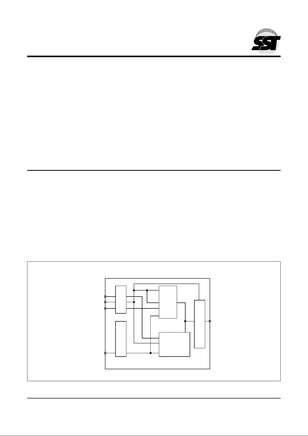
RAMCS#
OE#/RAMCS#
ROMCS#
WE#
AMS-A
0
Note: A
MS
= Most Significant Address
DQ7-DQ
0
ROMCS#
RAM
ROM
WE#
OE#
OE#
381 ILL B1.2
Control
Circuit
Address Buffer
Data Buffer
FUNCTIONAL BLOCK DIAGRAM
4 Mbit ROM + 1 Mbit / 256 Kbit SRAM ROM/RAM Combo
SST30VR041 / SST30VR043
SST30VR041/0434 Mb Mask ROM (x8) + 1 Mb / 256 Kbit SRAM (x8) Combo
Page 2
2
Preliminary Specifications
4 Mbit ROM + 1 Mbit / 256 Kbit SRAM ROM/RAM Combo
SST30VR041 / SST30VR043
©2001 Silicon Storage Technology, Inc. S71134-02-000 4/01 381
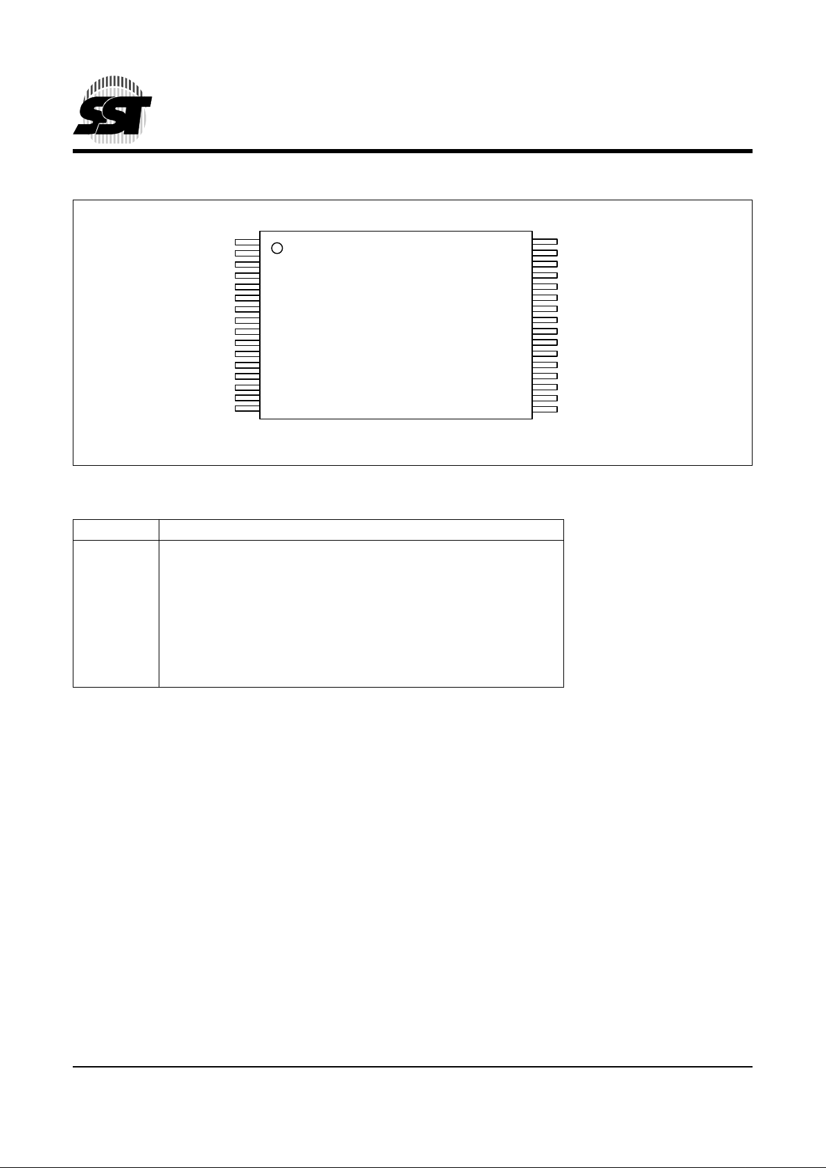
FIGURE 1: PIN ASSIGNMENTS FOR 32-PIN TSOP
TABLE 1: P
IN DESCRIPTION
Symbol Pin Name
A
MS
1
-A
0
1. AMS = Most significant address
Address Inputs, for ROM: AMS = A18, for RAM: AMS =A16 for SST30VR041
A
14
for SST30VR043
WE# Write Enable Input
OE#/RAMCS# Output Enable/RAM Enable Input
ROMCS# ROM Enable Input
DQ
7
-DQ
0
Data Input/Output
V
DD
Power Supply
V
SS
Ground
T1.2 381
A11
A9
A8
A13
A14
A17
WE#
V
DD
A18
A16
A15
A12
A7
A6
A5
A4
1
2
3
4
5
6
7
8
9
10
11
12
13
14
15
16
OE#/RAMCS#
A10
ROMCS#
DQ7
DQ6
DQ5
DQ4
DQ3
V
SS
DQ2
DQ1
DQ0
A0
A1
A2
A3
32
31
30
29
28
27
26
25
24
23
22
21
20
19
18
17
381 ILL F01.0
Standard Pinout
T op Vie w
Die Up
Page 3
Preliminary Specifications
4 Mbit ROM + 1 Mbit / 256 Kbit SRAM ROM/RAM Combo
SST30VR041 / SST30VR043
3
©2001 Silicon Storage Technology, Inc. S71134-02-000 4/01 381
Absolute Maximum Stress Ratings (Applied conditions greater than those listed under “Absolute Maximum
Stress Ratings” may cause pe r manent dama ge to the device. This is a stres s rating only and funct ional operatio n
of the device at these conditions or conditions greater tha n those defined in the ope rational sections of this data
sheet is not implied. Exposure to absolute maximum stress rating conditions may affect device reliability.)
Operating Temperature . . . . . . . . . . . . . . . . . . . . . . . . . . . . . . . . . . . . . . . . . . . . . . . . . . . . . . . . . . . -20°C to +85°C
Storage Temperature . . . . . . . . . . . . . . . . . . . . . . . . . . . . . . . . . . . . . . . . . . . . . . . . . . . . . . . . . . . -65°C to +150°C
Voltage on Any Pin Relative to V
SS
. . . . . . . . . . . . . . . . . . . . . . . . . . . . . . . . . . . . . . . . . . . . . . .-0.5V to VDD + 0.5V
Voltage on V
DD
Supply Relative to VSS . . . . . . . . . . . . . . . . . . . . . . . . . . . . . . . . . . . . . . . . . . . . . . . . . -0.5V to 4.0V
Power Dissipation. . . . . . . . . . . . . . . . . . . . . . . . . . . . . . . . . . . . . . . . . . . . . . . . . . . . . . . . . . . . . . . . . . . . . . . . 1.0W
Soldering Temperature (10 Seconds Lead Only) . . . . . . . . . . . . . . . . . . . . . . . . . . . . . . . . . . . . . . . . . . . . . . 260°C
O
PERATING RANGE
Range Ambient Temp V
DD
Commercial 0°C to +70°C 2.7-3.3V
Extended -20°C to +85°C 2.7-3.3V
AC CONDITIONS OF TEST
Input Pulse Lev el. . . . . . . . . . . . . . . . . . . . 0-V
DD
Input & Output Timing Reference Levels . . . VDD/2
Input Rise/Fall Time . . . . . . . . . . . . . . . . . . . 5 ns
Output Load . . . . . . . . . . . . . . . . . . . . . . . . . C
L
= 30 pF for 70 ns
Output Load . . . . . . . . . . . . . . . . . . . . . . . . . C
L
= 100 pF for 150 ns
TABLE 2: RECOMMENDED DC OPERATING CONDITIONS
Symbol Parameter Min Max Units
V
DD
Supply Voltage 2.7 3.3 V
V
SS
Ground 0 0 V
V
IH
Input High Voltage 2.4 VDD + 0.5 V
V
IL
Input Low Voltage -0.3 0.3 V
T2.0 381
TABLE 3: DC OPERATING CHARACTERISTICS
Symbol Parameter
V
DD
= 3.0±0.3V
Test ConditionsMin Max Units
I
DD1
ROM Operating Supply Current 4.0+1.1(f)
1
1. f = Frequency of operation (MHz) = 1/cycle time
mA ROMCS# = VIL, RAMCS# = VIH,
V
IN
= VIH or V
IL, II/O
= Opens
I
DD2
RAM Operating Supply Current 2.5+1(f)
1
mA ROMCS# = VIH, RAMCS# = VIL, I
I/O
= Opens
I
SB
Standby VDD Current 10 µA ROMCS# ≥ VDD-0.2V, RAMCS# ≥ VDD-0.2V
V
IN
≥ VDD-0.2V or VIN ≤ 0.2V
I
LI
Input Leakage Current -1 1 µA VIN = VSS to V
DD
I
LO
Output Leakage Current -1 1 µA ROMCS# = RAMCS# = VIH or OE# = VIH or
WE# = V
IL
, V
I/O
= VSS to V
DD
V
OL
Output Low Voltage 0.4 V IOL = 1.0 mA
V
OH
Output High Voltage 2.2 V IOH = -0.5 mA
T3.4 381
Page 4

4
Preliminary Specifications
4 Mbit ROM + 1 Mbit / 256 Kbit SRAM ROM/RAM Combo
SST30VR041 / SST30VR043
©2001 Silicon Storage Technology, Inc. S71134-02-000 4/01 381
FIGURE 2: AC INPUT/OUTPUT REFERENCE WAVEFORMS
FIGURE 3: A TEST LOAD EXAMPLE
TABLE 4: CAPACITANCE (Ta = 25°C, f=1 Mhz)
Parameter Description Test Condition Maximum
C
I/O
1
I/O Pin Capacitance V
I/O
= 0V 8 pF
C
IN
1
Input Capacitance VIN = 0V 6 pF
T4.1 381
1. This parameter is measured only for initial qualification and after a design or process change that could affect this parameter.
381 ILL F07.0
REFERENCE POINTS OUTPUTINPUT
V
IT
V
IHT
V
ILT
V
OT
AC test inputs are driven at V
IHT
(0.9 VDD) for a logic “1” and V
IL T
(0.1 VDD) for a logic “0”. Measurement reference points
for inputs and outputs are V
IT
(0.5 VDD) and VOT (0.5 VDD). Input rise and fall times (10% ↔ 90%) are <5 ns.
Note: V
IT
- V
INPUT
Test
V
OT
- V
OUTPUT
Test
V
IHT
- V
INPUT
HIGH Test
V
ILT
- V
INPUT
LOW Test
381 ILL F08.0
TO TESTER
TO DUT
C
L
Page 5

Preliminary Specifications
4 Mbit ROM + 1 Mbit / 256 Kbit SRAM ROM/RAM Combo
SST30VR041 / SST30VR043
5
©2001 Silicon Storage Technology, Inc. S71134-02-000 4/01 381
AC CHARACTERISTICS
I. ROM Operation
FIGURE 4: ROM READ CYCLE TIMING DIAGRAM (ADDRESS CONTROLLED) (ROMCS# = OE# = VIL)
TABLE 5: R
EAD CYCLE TIMING PARAMETERS V
DD
= 3.0V±0.3
Symbol Parameter
SST30VR041-70 SST30VR041/043-150
UnitsMin Max Min Max
T
RC
Read Cycle Time 70 150 ns
T
AA
Address Access Time 70 150 ns
T
CO
Chip Select to Output 70 150 ns
T
OE
Output Enable to Valid Output 35 70 ns
T
LZ
Chip Select to Low-Z Output 0 0 ns
T
OLZ
Output Enable to Low-Z Output 0 0 ns
T
HZ
Chip Disable to High-Z Output 25 30 ns
T
OHZ
Output Disable to High-Z Output 25 30 ns
T
OH
Output Hold from Address Change 10 15 ns
T5.2 381
T
RC
T
AA
Data Valid
381 ILL F02.0
Data Out Previous Data Valid
Address
T
OH
Page 6

6
Preliminary Specifications
4 Mbit ROM + 1 Mbit / 256 Kbit SRAM ROM/RAM Combo
SST30VR041 / SST30VR043
©2001 Silicon Storage Technology, Inc. S71134-02-000 4/01 381
FIGURE 5: ROM READ CYCLE TIMING DIAGRAM (ROMCS# & OE# CONTROLLED)
II. SRAM Operation (ROMCS# = V
IH
)
T
RC
T
AA
T
CO
T
LZ(2)
T
OHZ(1)
T
OH
T
HZ(1,2)
Data Valid
381 ILL F03.0
Data Out
OE#
ROMCS#
High-Z
Address
T
OE
T
OLZ
Notes: 1. THZ and T
OHZ
are defined as the time at which the outputs achieve the open circuit condition
and are referenced to the VOH or VOL.
2. At any given temperature and voltage condition THZ(max) is less than TLZ(min) both for a given
device and from device to device.
TABLE 6: READ CYCLE TIMIN G PARAMETERS VDD = 3.0V±0.3
Symbol Parameter
SST30VR041-70 SST30VR041/043-150
UnitsMin Max Min Max
T
RC
Read Cycle Time 70 150 ns
T
AA
Address Access Time 70 150 ns
T
CO
Chip Select to Output 70 150 ns
T
LZ
Chip Select to Low-Z Output 0 0 ns
T
HZ
Chip Disable to High-Z Output 25 30 ns
T
OH
Output Hold from Address Change 10 15 ns
T6.2 381
TABLE 7: WRITE CYCLE TIMING PARAMETERS VDD = 3.0V±0.3
Symbol Parameter
SST30VR041-70 SST30VR041/043-150
UnitsMin Max Min Max
T
WC
Write Cycle Time 70 150 ns
T
CW
Chip Select to End-of-Write 60 120 ns
T
AW
Address Valid to End-of-Write 60 120 ns
T
AS
Address Set-up Time 0 0 ns
T
WP
Write Pulse Width 60 120 ns
T
WR
Write Recovery Time 0 0 ns
T
WHZ
Write to Output High-Z 30 60 ns
T
DW
Data to Write Time Overlap 30 60 ns
T
DH
Data Hold from Write Time 0 0 ns
T
OW
End Write to Output Low-Z 0 10 ns
T7.2 381
Page 7

Preliminary Specifications
4 Mbit ROM + 1 Mbit / 256 Kbit SRAM ROM/RAM Combo
SST30VR041 / SST30VR043
7
©2001 Silicon Storage Technology, Inc. S71134-02-000 4/01 381
FIGURE 6: SRAM READ CYCLE TIMING DIAGRAM (ADDRESS CONTROLLED) (OE#/RAMCS# = VIL, WE# = VIH)
FIGURE 7: SRAM R
EAD CYCLE TIMING DIAGRAM (OE#/RAMCS# CONTROLLED)
T
RC
T
AA
Data Valid
381 ILL F04.0
Data Out Previous Data Valid
Address
T
OH
T
RC
T
AA
T
CO
T
LZ(2)
T
OH
T
HZ(1,2)
Data Valid
381 ILL F05.0
Data Out
OE#/RAMCS#
High-Z
Address
Notes: 1. THZ and T
OHZ
are defined as the time at which the outputs achieve the open circuit condition
and are referenced to the VOH or VOL.
2. At any given temperature and voltage condition THZ(max) is less than TLZ(min) both for a given
device and from device to device.
3. WE# is high for Read cycle.
Page 8

8
Preliminary Specifications
4 Mbit ROM + 1 Mbit / 256 Kbit SRAM ROM/RAM Combo
SST30VR041 / SST30VR043
©2001 Silicon Storage Technology, Inc. S71134-02-000 4/01 381
FIGURE 8: SRAM WRITE CYCLE TIMING DIAGRAM
TABLE 8: FUNCTIONAL DESCRIPTION/TRUTH TABLE
Address Inputs ROMCS#
OE#/RAMCS#
1
(Pin 32)
1. OE# & RAMCS# are pin-shared
WE# DQ7-DQ
0
X
2
2. X means Don’t Care.
H H X Z Standby
A
MS
3
-A
0
3. For ROM: AMS = A18 for SST30VR041 and SST30VR043
L OE# (H) X Z Output Floating
A
MS
3
-A
0
LOE# (L)XD
OUT
ROM Read
Only A
MS
4
-A0 are valid
4. For RAM: AMS = A16 for SST30VR041, A18-A17 must be fixed to “L” or “H”
A
MS
= A14 for SST30VR043, A18-A15 must be fixed to “L” or “H”
HRAMCS# (L)HD
OUT
RAM Read
Only A
MS
4
-A0 are valid H RAMCS# (L) L D
IN
RAM Write
T8.3 381
T
WC
T
AW
T
CW(2)
T
OH
T
DH
T
DW
T
OW
T
WR(4)
Data Valid
381 ILL F06.0
Data In
Data Out
WE#
OE#/RAMCS#
High-Z
High-Z (6)
(7) (8)
Address
T
WP(1)
T
AS(3)
T
WHZ(5)
Notes: 1. A write occurs during the overlap (TWP) of a low RAMCS# and low WE#. A write begins at the latest transition among
RAMCS# going low and WE# going low: A write end at the earliest transition among RAMCS# going high and WE# going high,
TWP is measured from the beginning of write to the end of write.
2. TCW is measured from the later of RAMCS# going low to the end of write.
3. TAS is measured from the address valid to the beginning of write.
4. TWR is measured from the end of write to the address change.
5. If RAMCS#, WE# are in the read mode during this period, the I/O pins are in the outputs Low-Z state.
Inputs of opposite phase of the output must not be applied because bus contention can occur.
6. If RAMCS# goes low simultaneously with WE# going low or after WE# going low, the outputs remain high impedance state.
7. D
OUT
is the same phase of the latest written data in this write cycle.
8. D
OUT
is the read data of new address
9. ROMCS# = V
IH
Page 9

Preliminary Specifications
4 Mbit ROM + 1 Mbit / 256 Kbit SRAM ROM/RAM Combo
SST30VR041 / SST30VR043
9
©2001 Silicon Storage Technology, Inc. S71134-02-000 4/01 381
SST30VR041 Valid combinations
SST30VR041-70-C-WH
SST30VR041-150-C-WH
SST30VR041-70-C-U1
SST30VR041-150-C-U1
SST30VR041-70-E-WH
SST30VR041-150-E-WH
SST30VR043 Valid combinations
SST30VR043-150-C-WH
SST30VR043-150-C-U1
SST30VR043-150-E-WH
Example: Valid combinations are those products in mass production or will be in mass production. Consult your SST sales
representative to confirm availability of valid combinations and to determine availability of new combinations.
C-Spec Number
Package Modifie r
H = 32 leads
Numeric = Die modifier
Package Type
W = TSOP (8mm x 14mm)
U = Die only
Temperature Range
C = Commercial = 0°C to +70°C
E = Extended = -20°C to +85°C
Read Access Speed
70 = 70 ns
150 = 150 ns
Device Density
041 = 4 Mbit R OM + 1 Mbit SRAM
043 = 4 Mbit ROM + 256 Kbit SRAM
Voltage Range
V = 2.7-3.3V
Device Family
30 = ROM/RAM Combo
Device Speed Suffix1 Suffix2
SST30
VR0xx -XXX -X -XX - RXXXX
Page 10

10
Preliminary Specifications
4 Mbit ROM + 1 Mbit / 256 Kbit SRAM ROM/RAM Combo
SST30VR041 / SST30VR043
©2001 Silicon Storage Technology, Inc. S71134-02-000 4/01 381
PACKAGING DIAGRAMS
32-PIN THIN SMALL OUTLINE PACKAGE (TSOP) 8MM X 14MM
SST PACKAGE CODE: WH
32.TSOP-WH-ILL.4
Note: 1. Complies with JEDEC publication 95 MO-142 BA dimensions, although some dimensions may be more stringent.
2. All linear dimensions are in millimeters (min/max).
3. Coplanarity: 0.1 (±.05) mm.
4. Maximum allowable mold flash is 0.15mm at the package ends, and 0.25mm between leads.
8.10
7.90
.270
.170
1.05
0.95
.50
BSC
0.15
0.05
12.50
12.30
Pin # 1 Identifier
14.20
13.80
0.70
0.50
Silicon Storage Technology, Inc. • 1171 Sonora Court • Sunnyvale , CA 940 86 • Telephone 408-735-9110 • Fax 408-735 -90 36
www.SuperFlash.com or www.ssti.com
 Loading...