

Datasheet SST28VF040A-90-4I-WH, SST28VF040A-90-4I-PH, SST28VF040A-90-4I-NH, SST28VF040A-90-4I-EH, SST28VF040A-90-4C-WH Datasheet (Silicon Storage Technology)
...Page 1

©2001 Silicon Storage Technology, Inc.
S71077-04-000 6/01 310
1
The SST logo and SuperFlash are registered trademarks of Silicon Storage Technology, Inc.
SSF is a trademark of Silicon Storage Technology, Inc.
These specifications are subject to change without notice.
Data Sheet
4 Mbit (512K x8) SuperFlash EEPROM
SST28SF040A / SST28VF040A
FEATURES:
• Single Voltage Read and Write Operations
– 5.0V-only for SS T28SF040A
– 2.7-3.6V for SST28VF040A
• Superior Reliability
– Endurance: 100,000 Cycles (typical)
– Greater than 100 years Data Retention
• Memory Organization: 512K x8
• Sector-Erase Capability: 256 Bytes per Sector
• Low Power Consumption
– Ac ti ve Current: 15 mA (typical) for 5.0V and
10 mA (typical) for 2.7-3.6V
– Standby Current: 5 µA (typical)
• Fast Sector-Erase/Byte-Program Operation
– Byte-Program Time: 35 µs (typical)
– Sector-Erase Time: 2 ms (typical)
– Complete Memory Rewrite: 20 sec (typical)
• Fast Read Access Time
– 5.0V-only operation: 90 and 120 ns
– 2.7-3.6V operation: 150 and 200 ns
• Latched Address and Data
• Hardware and Software Data Protection
– 7-Read-Cycle-Sequence Software Data
Protection
• End-of-Write Detection
– Toggle Bit
– Data# Polling
• TTL I/O Compatibility
• JEDEC Standard
– F lash EE PROM Pino uts
• Packages Available
– 32-lead PLCC
– 32-lead TSOP (8mm x 14mm and 8mm x 20mm)
– 32-pin PDIP
PRODUCT DESCRIPTION
The SST28SF/VF040A are 512K x8 bit CMOS SectorErase, Byte-Program EE PROMs. The SST28SF/VF0 40A
are manufactured using SST’s proprietary, high perfor-
mance CMOS SuperFlash EEPROM Technology. The
split-gate cell design and thick oxide tunneling injector
attain better reliability and manufacturability compared with
alternative approa c hes. Th e S ST2 8S F /V F04 0A erase an d
program with a single power supply. The SST28SF/
VF040A conform to JEDEC stan da rd pi no u ts for byte wide
memories and are compatible with existing industry standard flash EEPROM pinouts.
Featuring high perfor mance programming, the SST 28SF/
VF040A typically Byte-Program in 35 µs. The SST28SF/
VF040A typically Sector-Erase in 2 ms. Both Program and
Erase times can be optimized using interface features such
as Toggl e bi t or Da ta# Polling to indicat e th e c omp le ti on o f
the Write cycle. To protect agai nst an inadvertent write, the
SST28SF/VF040A have on chip hardware and Software
Data Protection schemes. Designed, manufactured, and
tested for a wide spectr um of appli cations, the SST2 8SF/
VF040A are offered with a guaranteed sector endurance of
10,000 cycles. Data retention is rated greater than 100
years.
The SST28SF/VF040A are best suited for applications that
require repro grammable nonvolatile mass storag e of program, configuration, or data memory. For all system appli-
cations, the SST28SF/VF040A significantly improve
performanc e and relia bility, while low ering pow er consu mption when compared with floppy diskettes or EPROM
approaches. Flash EEPROM technology makes possible
convenient and economical updating of codes and control
programs on-line. The SST28 SF/VF040A improve flexibility, while lowering the cost of program and configuration
storage application.
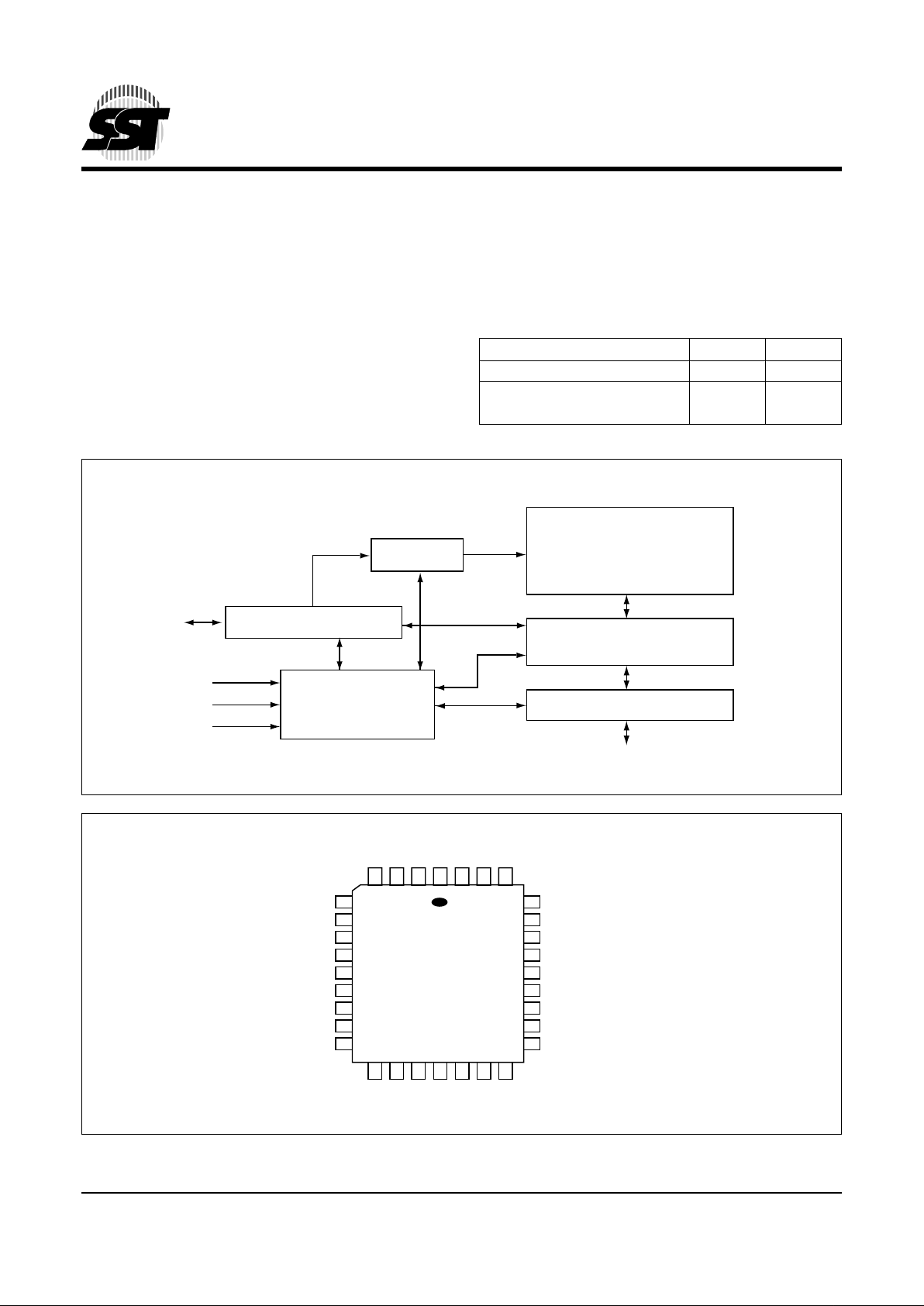
The functional block diagram shows the functional blocks of
the SST28SF/VF040A. Figures 1, 2, and 3 show the pin
assignments for the 32-lead PLCC, 32-lead TSOP, and 32pin PDIP packages. Pin descriptions and operation modes
are described in T ab les 2 through 5.
Device Operation
Commands are used to initiate the memory operation functions of the device. Commands ar e written to the device
using standard mi croprocessor write sequen ces. A command is written by asse r ting WE# low whil e keeping CE#
low. The address bus is latched on the falling edge of WE#
or CE#, whichever occurs last. T he data bus is latche d on
the rising edge of WE# or CE#, whichever occurs first.
Note, during the Software Da ta Protection sequence the
addresses are latche d on the r ising edge of OE# or CE#,
whicheve r occurs first.
SST28SF040A / SST28VF040A5.0 & 2.7 4Mb (x8) Byte-Program, Small Erase Sector flash memories
Page 2

2
Data Sheet
4 Mbit SuperFlash EEPROM
SST28SF040A / SST28VF040A
©2001 Silicon Storage Technology, Inc. S71077-04-000 6/01 310
Command Definitions
Table 4 contai ns a command list and a brief summar y of
the commands. The following is a detailed description of
the operations initiated by each command.
Sector-Erase Operation
The Sector-Erase operation erases all bytes within a sector
and is initiated by a setu p c om man d a nd a n execute command. A sector co nta in s 25 6 B y tes. Th is s ec to r erasa bi li ty
enhances the flexibility and usefulness of th e SST28SF/
VF040A, since most applications only ne ed to change a
small number of bytes or sectors, not the entire chip.
The setup command is perfor med by writing 20H to the
device. The execute command is performed by writing D0H
to the device. The Erase operatio n begins with the risin g
edge of the WE# or CE#, whichever occurs first and terminates automatically by using an internal timer. The End-ofErase can be deter min ed using eit her Data# Polling, Toggle Bit, or Successive Reads det ection metho ds. See Figure 9 for timing waveforms.
The two-step se quence of a se tup command followed by
an execute command ensures that only memory contents
within the addresse d sector are erased a nd other sectors
are not inadvertently erased.
Sector-Erase Flowchart Description
Fast and reliable erasing of the memor y cont ents with in a
sector is accomplished by following the Sector-Erase flowchart as shown in Figure 18. The entire procedure consists
of the execution of two commands. The Sector-Erase operation will termin ate after a maximum of 4 ms. A Re set command can be executed to terminate the Sector-Erase
operation; however, if the Erase operation is terminated
prior to the 4 ms time-out, the sector may not be fully
erased. A Sector-Erase command can be reissued as
many times as necessary to complete the Erase operation.
The SST28SF /VF040 A cannot be o ve r-er ased.
Chip-Erase Operation
The Chip-Erase operation is initiated by a setup command
(30H) and an execute comma nd (30H). The Chip-Erase
operation allows the en tire array of the SS T28SF/ VF040A
to be era sed i n on e op er a t ion, a s op po se d t o 20 48 Se ct o rErase operations. Using the Chip-Erase operation will minimize the time to rewrite the entire memory array. The ChipErase operation will terminate after a maximum of 20 ms. A
Reset command ca n be executed to termina te the Erase
operation; however, if the Chip-Erase operation is terminated prior to the 20 ms time-out, the chip may not be completely erased. If an erase error occurs a Chip-Erase
command can be rei ssued as many times as nece ssary to
complete the Chip-Erase operation. The SST28SF/
VF040A cannot be o ve r-er ased. ( See Fig ure 8)
Byte-Progr am Op eration
The Byte-Prog ram op eratio n is init iated b y writing th e setup
command (10H). Once th e program setup is performed,
programming is executed by the next WE# pulse. See Figures 5 and 6 for timing waveforms. The address bus is
latched on the falling edge of WE# or CE#, whichever
occurs last. The data bus is latched on the ris ing edge of
WE# or CE#, w hichever occurs first, and begins the Program operation. The Program operation is terminated automatically by an internal timer. See Figure 16 for the
programming flowchart.
The two-step seque nce of a setup command followed by
an execute command ensures that only the addressed
byte is programmed and oth er bytes are not i nadvert ently
programmed.
The Byte-Program Flowchart Description
Programming data in to the SST28SF/VF040A is accomplished by following the Byte-Pr ogram flowchar t shown in
Figure 16. The Byte-P rogram command sets up the byte
for programming. The address bus is latched on the falling
edge of WE# or CE#, whichever occurs last. The data bus
is latched on the r ising edge of WE# or CE#, whichever
occurs first and b egi ns the Program operation. T h e end o f
program can be detected using either the Data# Polling,
Toggle bit, or Successiv e read s.
Reset Operation
The Reset command is provided as a means to safely
abort the Erase or Program command sequences. Following either setup commands (Erase or Program) with a write
of FFH will safely abort the operation. Memory contents will
not be altered. After the Reset command, the device
returns to the Read m ode. The Res et co mmand do es no t
enable Software Data Pr otection. See Figure 7 for timing
waveforms.
Read
The Read operation is initiated by setting CE#, and OE# to
logic low and setting WE # to log ic hi gh (See Table 3). See
Figure 4 for Read cycle timing waveform. The Read operation from the host retrieves data from the array. The device
remains enabled for Read until an other operati on mode is
accessed. Durin g initia l po wer- up , the de vice i s in th e Read
mode and is Software Data protected. The device must be
unprotected to execute a Write command.
Page 3

Data Sheet
4 Mbit SuperFlash EEPROM
SST28SF040A / SST28VF040A
3
©2001 Silicon Storage Technology, Inc. S71077-04-000 6/01 310
The Read operation of the SST28SF/VF040A are controlled by OE# and CE# at logic low. When CE # is high,
the chip is deselected and only standby power will be consumed. OE# is the out put co ntr o l a nd i s used to gate data
from the output p ins. The data bus is in hi gh impedance
state when CE# or OE# are high.
Read-ID operation
The Read-ID operation is initiated by writing a single command (90H). A read of address 0000H will output the manufacturer’s ID (BFH). A read of address 00 01H will output
the device ID (04H). Any other valid command will ter minate this operation.
Data Protection
In order to protect th e integri ty of nonvolatile data s torage,
the SST28SF/VF040A provide both
hardware and software features to prevent inadvertent
writes to the device, for example, during system power-up
or power-down. Such provisions are described below.
Hardware Data Protection
The SST28SF/VF040A are designed with hardware features to prevent inadverte nt write s. This is done i n the following w ays:
1. Write Cycle Inhibit Mode:
OE# low, CE#, or WE#
high will inhibit the Write operation.
2. Noise/G litch Prot ection: A WE# pulse width of less
than 5 ns will not initiate a Write cycle.
3. V
DD
Power Up/Down Detection: The Write opera-
tion is inhibited when V
DD
is less than 2.0V.
4. After power-up, the device is in the Read mode
and the device is in the Software Data Protect
state.
Software Data Protection (SDP)
The SST28SF/VF04 0A have software methods to fur ther
prevent inadvertent wri tes. In o rder to pe rform an Era se or
Program operation, a two-step command seq uence consisting of a set -up comma nd followed by an execute command avoids inadvertent erasing and programming of the
device .
The SST28SF/VF0 40A will default to Software Data Protection after power up. A sequence of seven consecutive
reads at speci fic addresses will unprotect the device Th e
address sequence is 1823H, 1820H, 1822H, 0418H,
041BH, 0419H, 041AH. The address bus is latched on the
rising edge of OE# or CE#, whichever occurs first. A similar
seven read sequence of 1823H, 1820H, 18 22H, 0418H,
041BH, 0419H, 040AH will protect the device. Also refer to
Figures 10 and 11 for the 7 read cycle sequence Software
Data Protec tion. The I/O pins c an be in any state ( i.e ., hi gh,
low , or tri-stat e).
Write Operation Status Detection
The SST28SF/VF040 A provide three me ans to detec t the
completion of a Wr ite operation, in order to optimize th e
system Write operation. The end of a Write operation
(Erase or Program ) can be detected by t hree means: 1)
monitoring the Dat a# Polling bit, 2) monitoring the Toggle
bit, or 3) by two successiv e re ad s of t he sa me dat a. Th ese
three detection mechanisms are described below.
The actual completion of the nonvolatile Write is asynchronous with the system ; therefore, either a Data# Polling or
Toggle Bit read may be simultan eous with the co mpletion
of the Write cycle. If this occurs, the system may possibly
get an erroneous result, i.e., valid data may appear to conflict with the DQ used. In order to pr event spurious rejection, if an erroneous result occurs, the software routine
should include a loop to read the accessed location an
additional two (2) times. If bo th reads are valid, then the
device has completed the Write cycle, otherwise the rejection is valid.
Data# Polling (DQ7)
The SST28SF/VF040A feature Data# Polling to indicate
the Write ope ration status. During a Write operation, any
attempt to read the last byte loaded during the byte-load
cycle will receive the complement of the true data on DQ
7
.
Once the Write cycle is completed, DQ
7
will show true
data. The device is then re ady for the next operation. See
Figure 12 for Data# Polling timing waveforms. In order for
Data# Polling to function correctly, the byte being polled
must be erased prior to programming.
Toggle Bit (DQ6)
An alternati ve means for determining the Write operation
status is by monitoring the Toggle Bit, DQ
6
. During a Write
operation, consecutive attempts to read data from the
device will re sult in DQ
6
toggling between logic 0 (low) and
logic 1 (high). When the Wri te cycl e is comp leted, the toggling will stop. The device is then ready for the next operation. See Figure 13 for Toggle Bit timing waveforms.
Page 4
4
Data Sheet
4 Mbit SuperFlash EEPROM
SST28SF040A / SST28VF040A
©2001 Silicon Storage Technology, Inc. S71077-04-000 6/01 310
Successive Reads
An Alternative means for determining an end of a write
operation is by reading the same address for two consecutive data matches.
Product Identification
The Product Identification mode identifies the device as
SST28SF/VF040A and the manufacturer as SST. This
mode may be accessed by hardware and software operations. The hardware operation is typically used by an external programmer to identify the correct algorithm for the
SST28SF/VF040A. Users may wish to use the software
operation to ident ify the device (i.e., using the device ID ).
For de tai l s see Tabl e 3 for the hardware operation and Fi gure 19 for the software operation. The ma nufacturer and
device IDs are the same for both operations.
FIGURE 1: P
IN ASSIGNMENTS FOR 32-LEAD PLCC
TABLE 1: P
RODUCT IDENTIFICATION
Address Data
Manufacturer’s ID 0000H BFH
Device ID
SST28SF/VF040A 0001H 04H
T1.1 310
Y-Decoder
I/O Buffers and Data Latches
310 ILL B1.1
Address Buffer & Latches
X-Decoder
DQ7 - DQ
0
A18 - A
0
WE#
OE#
CE#
SuperFlash
Memory
Control Logic
FUNCTIONAL BLOCK DIAGRAM
5
6
7
8
9
10
11
12
13
29
28
27
26
25
24
23
22
21
A7
A6
A5
A4
A3
A2
A1
A0
DQ0
A14
A13
A8
A9
A11
OE#
A10
CE#
DQ7
4 3 2 1 32 31 30
A12
A15
A16
A18
VDDWE#
A17
32-lead PLCC
T op Vie w
310 ILL F02.3
14 15 16 17 18 19 20
DQ1
DQ2
V
SS
DQ3
DQ4
DQ5
DQ6
Page 5
Data Sheet
4 Mbit SuperFlash EEPROM
SST28SF040A / SST28VF040A
5
©2001 Silicon Storage Technology, Inc. S71077-04-000 6/01 310
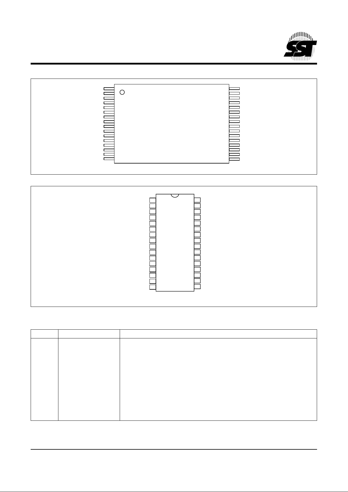
FIGURE 2: PIN ASSIGNMENTS FOR 32-LEAD TSOP
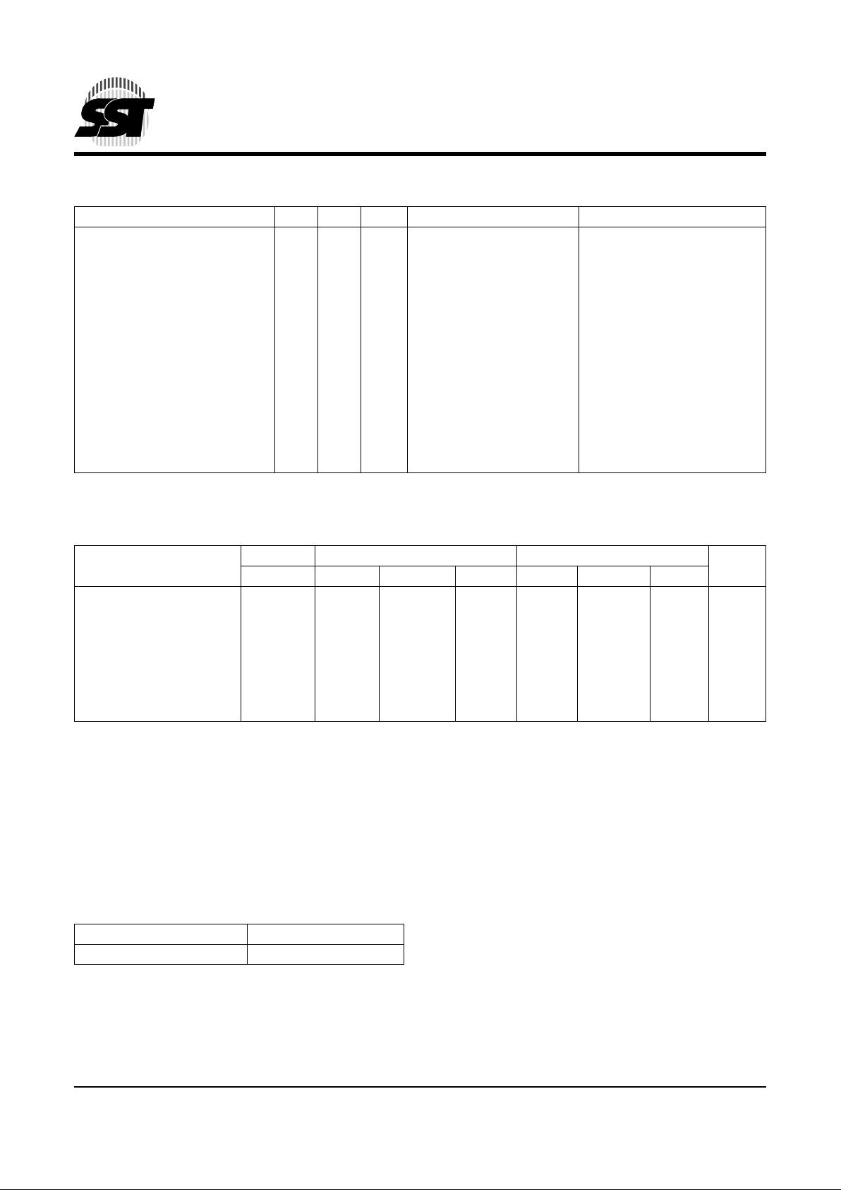
FIGURE 3: P
IN ASSIGNMENTS FOR 32-PIN PDIP
A11
A9
A8
A13
A14
A17
WE#
V
DD
A18
A16
A15
A12
A7
A6
A5
A4
1
2
3
4
5
6
7
8
9
10
11
12
13
14
15
16
OE#
A10
CE#
DQ7
DQ6
DQ5
DQ4
DQ3
V
SS
DQ2
DQ1
DQ0
A0
A1
A2
A3
32
31
30
29
28
27
26
25
24
23
22
21
20
19
18
17
310 ILL F01.2
Standard Pinout
T op Vie w
Die Up
1
2
3
4
5
6
7
8
9
10
11
12
13
14
15
16
32-pin
PDIP
T op Vie w
310 ILL F19.0
A18
A16
A15
A12
A7
A6
A5
A4
A3
A2
A1
A0
DQ0
DQ1
DQ2
V
SS
32
31
30
29
28
27
26
25
24
23
22
21
20
19
18
17
V
DD
WE#
A17
A14
A13
A8
A9
A11
OE#
A10
CE#
DQ7
DQ6
DQ5
DQ4
DQ3
TABLE 2: PIN DESCRIPTION
Symbol Pin Name Functions
A18-A
8
Row Address Inputs To provide memory addresses. Row addresses define a sector.
A7-A
0
Column Address Inputs Selects the byte within the sector
DQ
7
-DQ0Data Input/output To output data during Read cycles and receive input data during Write cycles.
Data is internally latched during a Write cycle.
The outputs are in tri-state when OE# or CE# is high.
CE# Chip Enable To activate the device when CE# is low.
1
OE# Output Enable To gate the data output buffers.
WE# Write Enable To control the Write operations.
1
V
DD
Power Supply To provide: 5.0V supply (±10%) for SST28SF040A
2.7V supply (2.7-3.6V) for SST28VF040A
V
SS
Ground
T2.2 310
1. This pin is internally pull-up with a resistor.
Page 6
6
Data Sheet
4 Mbit SuperFlash EEPROM
SST28SF040A / SST28VF040A
©2001 Silicon Storage Technology, Inc. S71077-04-000 6/01 310
TABLE 3: OPERATION MODES SELECTION
Mode CE# OE# WE# DQ Address
Read V
IL
V
IL
V
IH
D
OUT
A
IN
Byte-Program V
IL
V
IH
V
IL
D
IN
A
IN,
See Table 4
Sector-Erase V
IL
V
IH
V
IL
D
IN
A
IN,
See Table 4
Standby V
IH
X
1
X High Z X
Write Inhibit X V
IL
X High Z/ D
OUT
X
XXV
IH
High Z/ D
OUT
X
Software Chip-Erase V
IL
V
IH
V
IL
D
IN
See Table 4
Product Identification
Hardware Mode V
IL
V
IL
V
IH
Manufacturer’s ID (BFH)
Device ID (04H)
A18-A1=VIL, A9=VH, A0=V
IL
A18-A1=VIL, A9=VH, A0=V
IH
Software Mode V
IL
V
IL
V
IH
See Table 4
SDP Enable & Disable Mode V
IL
V
IL
V
IH
See Table 4
Reset V
IL
V
IH
V
IL
See Table 4
T3.4 310
1. X can be VIL or VIH, but no other value.
TABLE 4: SOFTWARE COMMAND SUMMARY
Command Summary
Required Setup Command Cycle Execute Command Cycle
Cycle(s) Type
1
1. Type definition: W = Write, R = Read, X can be VIL or VIH, but no other value.
Addr
2,3
2. Addr (Address) definition: SA = Sector Address = A18 - A8, sector size = 256 Bytes; A7- A0 = X for this command.
3. Addr (Address) definition: PA = Program Address = A
18
- A0.
Data
4
4. Data definition: PD = Program Data, H = number in hex.
Type
1
Addr
2,3
Data4SDP
5
5. SDP = Software Data Protect mode using 7 Read Cycle Sequence.
a) Y = the operation can be executed with protection enabled
b) N = the operation cannot be executed with protection enabled
Sector-Erase 2 W X 20H W SA D0H N
Byte-Program 2 W X 10H W PA PD N
Chip-Erase
6
6. The Chip-Erase function is not supported on SST28VF040A industrial parts.
2 W X 30H W X 30H N
Reset 1 W X FFH Y
Read-ID 2 W X 90H R
7
7. Address 0000H retrieves the Manufacturer’s I D of BFH and address 0001H retrieves the Device ID of 04H.
7
Y
Software Data Protect 7 R
8
8. Refer to Figure 11 for the 7 Read Cycle sequence for Software_Data_Protect.
Software Data Unprotect 7 R
9
9. Refer to Figure 10 for the 7 Read Cycle sequence for Software_Data_Unprotect.
T4.3 310
TABLE 5: MEMORY ARRAY DETAIL
Sector Select Byte Select
A
18
- A
8
A7 - A
0
T5.0 310
Page 7
Data Sheet
4 Mbit SuperFlash EEPROM
SST28SF040A / SST28VF040A
7
©2001 Silicon Storage Technology, Inc. S71077-04-000 6/01 310
Absolute Maximum Stress Ratings (Applied conditions greater than those listed under “Absolute Maximum
Stress Ratings” may cause pe r manent dama ge to the device. This is a stres s rating only and funct ional operatio n
of the device at these conditions or conditions greater tha n those defined in the ope rational sections of this data
sheet is not implied. Exposure to absolute maximum stress rating conditions may affect device reliability.)
Temperature Under Bias . . . . . . . . . . . . . . . . . . . . . . . . . . . . . . . . . . . . . . . . . . . . . . . . . . . . . . . . . -55°C to +125°C
Storage Temperature . . . . . . . . . . . . . . . . . . . . . . . . . . . . . . . . . . . . . . . . . . . . . . . . . . . . . . . . . . . -65°C to +150°C
D. C. Voltage on Any Pin to Ground Potential . . . . . . . . . . . . . . . . . . . . . . . . . . . . . . . . . . . . . . .-0.5V to V
DD
+ 0.5V
Transient Voltage (<20 ns) on Any Pin to Ground Potential . . . . . . . . . . . . . . . . . . . . . . . . . . . .-1.0V to V
DD
+ 1.0V
Voltage on A
9
Pin to Ground Potential . . . . . . . . . . . . . . . . . . . . . . . . . . . . . . . . . . . . . . . . . . . . . . . . -0.5V to 14.0V
Package Power Dissipation Capability (Ta = 25°C) . . . . . . . . . . . . . . . . . . . . . . . . . . . . . . . . . . . . . . . . . . . . . . 1.0W
Through Hold Lead Soldering Temperature (10 Seconds) . . . . . . . . . . . . . . . . . . . . . . . . . . . . . . . . . . . . . . . 300°C
Surface Mount Lead Soldering Temperature (3 Seconds) . . . . . . . . . . . . . . . . . . . . . . . . . . . . . . . . . . . . . . . 240°C
Output Short Circ uit Curr ent
1
. . . . . . . . . . . . . . . . . . . . . . . . . . . . . . . . . . . . . . . . . . . . . . . . . . . . . . . . . . . . 100 mA
1. Outputs shorted for no more than one second. No more than one output shorted at a time.
OPERATING RANGE FOR SST28S F040A
Range Ambient Temp V
DD
Commercial 0°C to +70°C5.0V±10%
Industrial -40°C to +85°C5.0V±10%
OPERATING RANGE FOR SST28V F040A
Range Ambient Temp V
DD
Commercial 0°C to +70°C 2.7-3.6V
Industrial -40°C to +85°C 2.7-3.6V
AC CONDITIONS OF TEST
Input Rise/Fall Time . . . . . . . . . . . . . . 10 ns
Output Load . . . . . . . . . . . . . . . . . . . . . 1 TTL Gate andC
L
= 100 pF for SST28SF040A
C
L
= 100 pF for SST28VF040A
See Figures 14 and 15
Page 8
8
Data Sheet
4 Mbit SuperFlash EEPROM
SST28SF040A / SST28VF040A
©2001 Silicon Storage Technology, Inc. S71077-04-000 6/01 310
TABLE 6: DC OPERATING CHARACTERISTICS FOR SS T2 8SF040A
Symbol Parameter
Limits
Test ConditionsMin Max Units
I
DD
Power Supply Current Address input=VIL/VIH, at f=1/TRC Min,
V
DD=VDD
Max
Read 32 mA CE#=OE#=V
IL
, WE#=VIH, all I/Os open
Program and Erase 40 mA CE#=WE#=V
IL
, OE#=VIH, VDD=VDD Max
I
SB1
Standby VDD Current
(TTL input)
3mACE#=VIH, VDD=VDD Max
I
SB2
Standby VDD Current
(CMOS input)
20 µA CE#=VDD-0.3V, VDD=VDD Max
I
LI
Input Leakage Current 1 µA VIN=GND to VDD, VDD=VDD Max
I
LO
Output Leakage Current 10 µA V
OUT
=GND to VDD, VDD=VDD Max
V
IL
Input Low Voltage 0.8 V VDD=VDD Min
V
IH
Input High Voltage 2.0 V VDD=VDD Max
V
OL
Output Low Voltage 0.4 V IOL=2.1 mA, VDD=VDD Min
V
OH
Output High Voltage 2.4 V IOH=-400 µA, VDD=VDD Min
V
H
Supervoltage for A
9
11.6 12.4 V CE#=OE#=VIL, WE#=V
IH
I
H
Supervoltage Current for A
9
200 µA CE#=OE#=VIL, WE#=VIH, A9=VH Max
T6.4 310
TABLE 7: DC OPERATING CHARACTERISTICS FOR SS T2 8VF040A
Symbol Parameter
Limits
Test ConditionsMin Max Units
I
DD
Power Supply Current Address input=VIL/VIH, at f=1/TRC Min,
V
DD=VDD
Max
Read 10 mA CE#=OE#=VIL, WE#=VIH, all I/Os open
Program and Erase 25 mA CE#=WE#=V
IL
, OE#=VIH, VDD=VDD Max
I
SB2
Standby VDD Current
(CMOS input)
20 µA CE#=OE#=WE#=VDD-0.3V, VDD=VDD Max
I
LI
Input Leakage Current 1 µA VIN=GND to VDD, VDD=VDD Max
I
LO
Output Leakage Current 10 µA V
OUT
=GND to VDD, VDD=VDD Max
V
IL
Input Low Voltage 0.8 V VDD=VDD Min
V
IH
Input High Voltage 2.0 V VDD=VDD Max
V
OL
Output Low Voltage 0.4 V IOL=100 µA, VDD=VDD Min
V
OH
Output High Voltage 2.4 V IOH=-100 µA, VDD=VDD Min
V
H
Supervoltage for A
9
11.6 12.4 V CE#=OE#=VIL, WE#=V
IH
I
H
Supervoltage Current for A
9
200 µA CE#=OE#=VIL, WE#=VIH, A9=VH Max
T7.4 310
Page 9

Data Sheet
4 Mbit SuperFlash EEPROM
SST28SF040A / SST28VF040A
9
©2001 Silicon Storage Technology, Inc. S71077-04-000 6/01 310
TABLE 8: RECOMMENDED SYSTE M POWER-UP TIMINGS
Symbol Parameter Minimum Units
T
PU-READ
1
Power-up to Read Operation 10 ms
T
PU-WRITE
1
Power-up to Write Operation 10 ms
T8.4 310
1. This parameter is measured only for initial qualification and after a design or process change that could affect this parameter.
TABLE 9: CAPACITANCE (Ta = 25°C, f=1 Mhz, other pins open)
Parameter Description Test Condition Maximum
C
I/O
1
1. This parameter is measured only for initial qualification and after a design or process change that could affect this parameter.
I/O Pin Capacitance V
I/O
= 0V 12 pF
C
IN
1
Input Capacitance VIN = 0V 6 pF
T9.0 310
TABLE 10: RELIABILITY CHARACTERISTICS
Symbol Parameter Minimum Specification Units Test Method
N
END
1
1. This parameter is measured only for initial qualification and after a design or process change that could affect this parameter.
Endurance 10,000 Cycles JEDEC Standard A117
T
DR
1
Data Retention 100 Years JEDEC Standard A103
I
LTH
1
Latch Up 100 + I
DD
mA JEDEC Standard 78
T10.7 310
Page 10

10
Data Sheet
4 Mbit SuperFlash EEPROM
SST28SF040A / SST28VF040A
©2001 Silicon Storage Technology, Inc. S71077-04-000 6/01 310
AC CHARACTERISTICS
TABLE 11: READ CYCLE TIMING PARAMETERS FOR SST28SF040A
IEEE
Symbol
Industry
Symbol Parameter
SST28SF040A-90 SST28SF040A-120
UnitsMin Max Min Max
tAVAV T
RC
Read Cycle Time 90 120 ns
tAVQV T
AA
Address Access Time 90 120 ns
tELQV T
CE
Chip Enable Access Time 90 120 ns
tGLQV T
OE
Output Enable Access Time 45 50 ns
tEHQZ T
CLZ
1
1. This parameter is measured only for initial qualification and after a design or process change that could affect this parameter.
CE# Low to Active Output 0 0 ns
tGHQZ T
OLZ
1
OE# Low to Active Output 0 0 ns
tELQX T
CHZ
1
CE# High to High-Z Output 20 30 ns
tGLQX T
OHZ
1
OE# High to High-Z Output 20 30 ns
tAXQX T
OH
1
Output Hold from Address Change 0 0 ns
T11.6 310
TABLE 12: READ CYCLE TIMING PARAMETERS FOR SST28VF040A
IEEE
Symbol
Industry
Symbol Parameter
SST28VF040A-150 SST28VF040A-200
UnitsMin Max Min Max
tAVAV T
RC
Read Cycle Time 150 200 ns
tAVQV T
AA
Address Access Time 150 200 ns
tELQV T
CE
Chip Enable Access Time 150 200 ns
tGLQV T
OE
Output Enable Access Time 75 100 ns
tEHQZ T
CLZ
1
1. This parameter is measured only for initial qualification and after a design or process change that could affect this parameter.
CE# Low to Active Output 0 0 ns
tGHQZ T
OLZ
1
OE# Low to Active Output 0 0 ns
tELQX T
CHZ
1
CE# High to High-Z Output 40 60 ns
tGLQX T
OHZ
1
OE# High to High-Z Output 40 60 ns
tAXQX T
OH
1
Output Hold from Address Change 0 0 ns
T12.5 310
Page 11

Data Sheet
4 Mbit SuperFlash EEPROM
SST28SF040A / SST28VF040A
11
©2001 Silicon Storage Technology, Inc. S71077-04-000 6/01 310
TABLE 13: ERASE/PROGRAM CYCLE TIMING PARAMETERS
IEEE
Symbol
Industry
Symbol Parameter
SST28SF040A SST28VF040A
UnitsMin Max Min Max
tAVA T
BP
Byte-Program Cycle Time 40 40 µs
tWLWH T
WP
Write Pulse Width (WE#) 90 100 ns
tAVWL T
AS
Address Setup Time 10 10 ns
tWLAX T
AH
Address Hold T ime 50 100 ns
tELWL T
CS
CE# Setup Time 0 0 ns
tWHEX T
CH
CE# Hold Time 0 0 ns
tGHWL T
OES
OE# High Setup Time 10 20 ns
tWGL T
OEH
OE# High Hold Time 10 20 ns
tWLEH T
CP
Write Pulse Width (CE#) 90 100 ns
tDVWH T
DS
Data Setup Time 50 100 ns
tWHDX T
DH
Data Hold Time 10 20 ns
tWHWL2 T
SE
Sector-Erase Cycle Time 4 4 ms
T
RST
1
Reset Command Recovery Time 4 4 µs
tWHWL3 T
SCE
Software Chip-Erase Cycle Time 20 20 ms
tEHEL T
CPH
CE# High Pulse Width 50 50 ns
tWHWL1 T
WPH
WE# High Pulse Width 50 50 ns
T
PCP
1
Protect CE# or OE# Pulse Width 50 50 ns
T
PCH
1
Protect CE# or OE# High Time 50 50 ns
T
PAS
1
Protect Address Setup Time 40 40 ns
T
PAH
1
Protect Address Hold Time 0 0 ns
T13.6 310
1. This parameter is measured only for initial qualification and after a design or process change that could affect this parameter.
Page 12

12
Data Sheet
4 Mbit SuperFlash EEPROM
SST28SF040A / SST28VF040A
©2001 Silicon Storage Technology, Inc. S71077-04-000 6/01 310
FIGURE 4: READ CYCLE TIMING DIAGRAM
FIGURE 5: WE# CONTROLLED BYTE-PROGRAM CYCLE TIMING DIAGRAM
310 ILL F03.2
CE#
ADDRESS A
18-0
OE#
WE#
DQ
7-0
T
CLZ
T
OH
DATA VALIDDATA VALID
T
OLZ
T
OE
T
CE
T
CHZ
T
OHZ
T
RC
T
AA
310 ILL F04.1
CE#
OE#
WE#
T
DH
T
DS
T
OES
T
CS
T
AS
T
AH
T
WP
T
WPH
T
OEH
T
CH
T
DS
T
DH
T
BP
ADDRESS A
18-0
DQ
7-0
BYTE-PROGRAM SETUP COMMAND
I0H
DATA VALID
Page 13

Data Sheet
4 Mbit SuperFlash EEPROM
SST28SF040A / SST28VF040A
13
©2001 Silicon Storage Technology, Inc. S71077-04-000 6/01 310
FIGURE 6: CE# CONTROLLED BYTE-PROGRAM CYCLE TIMING DIAGRAM
FIGURE 7: RESET COMMAND TIMING DIAGRAM
310 ILL F05.1
CE#
OE#
WE#
T
DH
T
DS
T
OES
T
CPH
T
AS
T
AH
T
CS
T
CH
T
OEH
T
CP
T
DS
T
DH
T
BP
ADDRESS A
18-0
DQ
7-0
BYTE-PROGRAM SETUP COMMAND
I0H
DATA VALID
310 ILL F06.0
CE#
OE#
WE#
T
DS
T
DH
T
RST
ADDRESS A
18-0
DQ
7-0
FFH
Page 14

14
Data Sheet
4 Mbit SuperFlash EEPROM
SST28SF040A / SST28VF040A
©2001 Silicon Storage Technology, Inc. S71077-04-000 6/01 310
FIGURE 8: CHIP-ERASE TIMING DIAGRAM
FIGURE 9: SECTOR-ERASE TIMING DIAGRAM
310 ILL F07.0
CE#
OE#
WE#
T
DH
T
DS
T
DH
T
SCE
T
DS
ADDRESS A
18-0
DQ
7-0
30H
SETUP
COMMAND
EXECUTE
COMMAND
30H
310 ILL F08.0
CE#
OE#
WE#
T
DH
T
AH
T
AS
A
IN
T
DS
T
DH
T
SE
T
DS
ADDRESS A
18-0
DQ
7-0
20H
SETUP
COMMAND
EXECUTE
COMMAND
D0H
Page 15

Data Sheet
4 Mbit SuperFlash EEPROM
SST28SF040A / SST28VF040A
15
©2001 Silicon Storage Technology, Inc. S71077-04-000 6/01 310
FIGURE 10: SOFTWARE DATA UNPROTECT DISABLE TIMING DIAGRAM
FIGURE 11: SOFTWARE DATA PROTECT DISABLE TIMING DIAGRAM
310 ILL F09.4
OE#
CE#
WE#
ADDRESS
T
PAH
T
PAS
T
PCH
T
PCP
NOTE: A. ADDRESSES ARE LATCHED INTERNALLY ON THE RISING EDGE OF:
1.OE# IF CE# IS KEPT AT LOW ALL TIME.
2.CE# IF OE# IS KEPT AT LOW ALL TIME.
3.THE FIRST PIN TO GO HIGH IF BOTH ARE TOGGLED.
B. ABOVE ADDRESS VALUES ARE IN HEX.
C. ADDRESSES > A12 ARE "DON'T CARE"
1823 1820 1822 0418 041B 0419 041A
310 ILL F10.4
OE#
CE#
WE#
ADDRESS
T
PAH
T
PAS
T
PCH
T
PCP
NOTE: A. ADDRESSES ARE LATCHED INTERNALLY ON THE RISING EDGE OF:
1.OE# IF CE# IS KEPT AT LOW ALL TIME.
2.CE# IF OE# IS KEPT AT LOW ALL TIME.
3.THE FIRST PIN TO GO HIGH IF BOTH ARE TOGGLED.
B. ABOVE ADDRESS VALUES ARE IN HEX.
C. ADDRESSES > A12 ARE "DON'T CARE"
1823 1820 1822 0418 041B 0419 040A
Page 16

16
Data Sheet
4 Mbit SuperFlash EEPROM
SST28SF040A / SST28VF040A
©2001 Silicon Storage Technology, Inc. S71077-04-000 6/01 310
FIGURE 12: DATA# POLLING TIM IN G DIAGRAM
FIGURE 13: TOGGLE BIT TIMING DIAGRAM
310 ILL F11.0
CE#
OE#
WE#
NOTE
D#
T
OE
T
OEH
T
CE
T
OES
D# D
ADDRESS A
18-0
DQ
7-0
NOTE: THIS TIME INTERVAL SIGNAL CAN BE TSE or TBP DEPENDING UPON THE SELECTED OPERATION MODE.
D
310 ILL F12.0
CE#
OE#
WE#
NOTE
TWO READ CYCLES
WITH SAME OUTPUTS
T
OEH
T
OE
T
OE
T
OES
T
CE
T
CE
ADDRESS A
18-0
DQ
6
NOTE: THIS TIME INTERVAL SIGNAL CAN BE TSE or TBP DEPENDING UPON THE SELECTED OPERATION MODE.
Page 17

Data Sheet
4 Mbit SuperFlash EEPROM
SST28SF040A / SST28VF040A
17
©2001 Silicon Storage Technology, Inc. S71077-04-000 6/01 310
FIGURE 14: AC INPUT/OUTPUT REFERENCE WAVEFORMS
FIGURE 15: A TEST LOAD EXAMPLE
310 ILL F13.1
REFERENCE POINTS OUTPUTINPUT
V
HT
V
LT
V
HT
V
LT
V
IHT
V
ILT
AC test inputs are driven at V
IHT
(2.4V) for a logic “1” and V
IL T
(0.4 V) for a logic “0”. Measuremen t reference poi nts for
inputs and outputs are V
HT
(2.0 V) and VLT (0.8 V). Input rise and fall times (10% ↔ 90%) are <10 ns.
Note: V
HT
- V
HIGH
Test
V
LT
- V
LOW
Test
V
IHT
- V
INPUT
HIGH Test
V
ILT
- V
INPUT
LOW Test
310 ILL F14.2
TEST LOAD EXAMPLE
TO TESTER
TO DUT
C
L
R
L LOW
RL
HIGH
V
DD
Page 18

18
Data Sheet
4 Mbit SuperFlash EEPROM
SST28SF040A / SST28VF040A
©2001 Silicon Storage Technology, Inc. S71077-04-000 6/01 310
FIGURE 16: BYTE-PROGRAM FLOWCHART
310 ILL F15.3
Yes
No
No
No
Last
Address
Read
End-of-Write
Detection
Yes
Data
Verifies?
Yes
Programming
Completed?
Programming
Completed
Next
Address
Programming
Failure
Load Address
and Data &
Start
Programming
Execute Byte-
Program Setup
Command
Initialize
Address
Start
Page 19

Data Sheet
4 Mbit SuperFlash EEPROM
SST28SF040A / SST28VF040A
19
©2001 Silicon Storage Technology, Inc. S71077-04-000 6/01 310
FIGURE 17: WRITE WAIT OPTIONS
310 ILL F16.2
No
No
Read byte
Yes
Yes
Does DQ
6
match?
Program/Erase
Completed
Read same
byte
Program/Erase
Initiated
Toggle Bit
Wait TBP or
T
SE
Program/Erase
Completed
Program/Erase
Initiated
Internal Timer
Read DQ
7
Is DQ7 =
true data?
Program/Erase
Completed
Program/Erase
Initiated
Data# Polling
Page 20

20
Data Sheet
4 Mbit SuperFlash EEPROM
SST28SF040A / SST28VF040A
©2001 Silicon Storage Technology, Inc. S71077-04-000 6/01 310
FIGURE 18: SECTOR-ERASE FLOWCHARTS
310 ILL F17.5
No
No
No
No
Yes
Yes
Yes
Yes
Last
Sector?
Verify
FFH
Erase
completed?
Last
Address?
Device
Erased
Execute Two Step
Sector-Erase
Command
Increment
Byte
Address
Next Sector
Address
End-of-Write
Detection
Read FFH from
Selected Byte
Address
Initialize
Sector Address
Start
Sector-Erase
Completed
Erase Error
Page 21

Data Sheet
4 Mbit SuperFlash EEPROM
SST28SF040A / SST28VF040A
21
©2001 Silicon Storage Technology, Inc. S71077-04-000 6/01 310
FIGURE 19: SOFTWARE PRODUCT ID FLOW
Execute Read ID
Command (90H) to
Enter Read-ID mode
Read Address 0000H
MFG's ID =
SST (BFH)
Read Address 0001H
Device ID =
28SF040 (04H)
Execute Reset
Command (FFH) to
Exit from
Read-ID mode
310 ILL F18.5
Page 22

22
Data Sheet
4 Mbit SuperFlash EEPROM
SST28SF040A / SST28VF040A
©2001 Silicon Storage Technology, Inc. S71077-04-000 6/01 310
PRODUCT ORDERING INFORMATION
Valid combinations for SST28SF040A
SST28SF040A-90-4C-NH SST28SF040A-90-4C-WH SST28SF040A-90-4C-EH SST28SF040A-90-4C-PH
SST28SF040A-120-4C-NH SST28SF040A-120-4C-WH SST28SF040A-120-4C-EH
SST28SF040A-120-4I-NH SST28SF040A-120-4I-WH SST28SF040A-120-4I-EH
Valid combinations for SST28VF040A
SST28VF040A-150-4C-NH SST28VF040A-150-4C-WH SST28VF040A-150-4C-EH
SST28VF040A-200-4C-NH SST28VF040A-200-4C-WH SST28VF040A-200-4C-EH
SST28VF040A-200-4I-NH SST28VF040A-200-4I-WH SST28VF040A-200-4I-EH
Note: Valid combinations are those products in mass production or will be in mass production. Consult your SST sales
representative to confirm availability of valid combinations and to determine availability of new combinations.
Note: The software Chip-Erase function is not supported by the industrial temperature part.
Please contact SST, if you require this function for an industrial temperature part.
Device Speed Suffix1 Suffix2
SST28x
F040A - XXX -XX -XX
Package Mo difier
H = 32 leads or pins
Package Type
N = PLCC
W = TSOP (die up) (8mm x 14mm)
E = TSOP (die up) (8mm x 20mm)
P = PDIP
Temperature Range
C = Commercial = 0°C to +70°C
I = Industrial = -40°C to +85°C
Minimum Endurance
4 = 10,000 cycles
Read Access Speed
200 = 200 ns
150 = 150 ns
120 = 120 ns
90 = 90 ns
Voltage
S = 4.5-5.5V
V = 2.7-3.6V
Page 23

Data Sheet
4 Mbit SuperFlash EEPROM
SST28SF040A / SST28VF040A
23
©2001 Silicon Storage Technology, Inc. S71077-04-000 6/01 310
PACKAGING DIAGRAMS
32-LEAD PLASTI C LEAD CHIP CARRIER (PLCC)
SST P
ACKAGE CODE: NH
32-
LEAD THIN SMALL OUTLINE PACKAGE (TSOP) 8MM X 14MM
SST PACKAGE CODE: WH
.030
.040
.013
.021
.490
.530
.075
.095
.015 Min.
.125
.140
TOP VIEW SIDE VIEW BOTTOM VIEW
1232
.026
.032
.400
BSC
32.PLCC.NH-ILL.2
Note: 1. Complies with JEDEC publication 95 MS-016 AE dimensions, although some dimensions may be more stringent.
2. All linear dimensions are in inches (min/max).
3. Dimensions do not include mold flash. Maximum allowable mold flash is .008 inches.
4. Coplanarity: 4 mils.
.050
BSC.
.050
BSC.
.026
.032
.023
.029
.447
.453
.042
.048
.042
.048
Optional
Pin #1 Identifier
.547
.553
.585
.595
.485
.495
.020 R.
MAX.
.106
.112
R.
x 30˚
32.TSOP-WH-ILL.4
Note: 1. Complies with JEDEC publication 95 MO-142 BA dimensions, although some dimensions may be more stringent.
2. All linear dimensions are in millimeters (min/max).
3. Coplanarity: 0.1 (±.05) mm.
4. Maximum allowable mold flash is 0.15mm at the package ends, and 0.25mm between leads.
8.10
7.90
.270
.170
1.05
0.95
.50
BSC
0.15
0.05
12.50
12.30
Pin # 1 Identifier
14.20
13.80
0.70
0.50
Page 24

24
Data Sheet
4 Mbit SuperFlash EEPROM
SST28SF040A / SST28VF040A
©2001 Silicon Storage Technology, Inc. S71077-04-000 6/01 310
32-LEAD THIN SMALL OUTLINE PACKAGE (TSOP) 8MM X 20MM
SST PACKAGE CODE: EH
32-
PIN PLASTIC DUAL-IN-LINE PACKAGE (PDIP)
SST P
ACKAGE CODE: PH
32.TSOP-EH-ILL.4
Note: 1. Complies with JEDEC publication 95 MO-142 BD dimensions, although some dimensions may be more stringent.
2. All linear dimensions are in millimeters (min/max).
3. Coplanarity: 0.1 (±.05) mm.
4. Maximum allowable mold flash is 0.15mm at the package ends, and 0.25mm between leads.
8.10
7.90
.27
.17
1.05
0.95
.50
BSC
0.15
0.05
18.50
18.30
20.20
19.80
0.70
0.50
Pin # 1 Identifier
32.pdipPH-ILL.2
Pin #1 Identifier
C
L
32
1
Base Plane
Seating Plane
Note: 1. Complies with JEDEC publication 95 MO-015 AP dimensions, although some dimensions may be more stringent.
2. All linear dimensions are in inches (min/max).
3. Dimensions do not include mold flash. Maximum allowable mold flash is .010 inches.
.170
.200
7˚
4 PLCS.
.600 BSC
.100 BSC
.120
.150
.016
.022
.045
.065
.070
.080
.015
.050
.065
.075
1.645
1.655
.008
.012
0˚
15˚
.600
.625
.530
.550
Silicon Storage Technology, Inc. • 1171 Sonora Court • Sunnyvale, CA 94086 • Telephone 408-735-9110 • Fax 408-735-90 36
www.SuperFlash.com or www.ssti.com
 Loading...