

Datasheet SST27SF512-90-3C-WH, SST27SF512-90-3C-WG, SST27SF512-90-3C-PH, SST27SF512-90-3C-PG, SST27SF512-90-3C-NH Datasheet (Silicon Storage Technology)
...Page 1

SST27SF256 / SST27SF512 / SST27SF010 / SST27SF020
SST27SF256 / 512 / 010 / 0205.0V-Read 256Kb / 512Kb / 1Mb / 2Mb (x8) MTP flash memories
FEATURES:
256 Kbit / 512 Kbit / 1 Mbit / 2 Mbit (x8)
Many-Time Programmable Flash
Data Sheet
• Organized as 32K x8 / 64K x8 / 128K x8 / 256K x8
• 4.5-5.5V Read Operation
• Superior Reliability
– Endurance: At least 1000 Cycles
– Greater than 100 years Data Retention
• Low Power Consumption
– Ac ti ve Current: 20 mA (typical)
– Standby Current: 10 µA (typical)
• Fast Read Access Time
– 70 ns
– 90 ns
PRODUCT DESCRIPTION
The SST27SF256/5 12/010/020 are a 32K x8 / 64K x8 /
128K x8 / 256K x8 CMOS, Many-Time Programmable
(MTP) low cost flas h, m an ufactured wi th SS T’s proprietary,
high performance SuperFlash technology. The split-gate
cell design and th ick oxide tunnelin g injector attain better
reliability and manufacturability compared with alternate
approaches. These MTP devices can be electrically erased
and programmed at least 1000 times using an external programmer with a 12 volt power supply. They have to be
erased prior to programming. These devices conform to
JEDEC standar d pino uts f or b yte -wide mem ories .
Featuring high performance Byte-Program, the
SST27SF256/512/010/020 provide a Byte-Program time of
20 µs. Designed, manufactured, and tested for a wide
spectrum of applications, these devices are offered with an
endurance of at least 1000 cycles. Data retention is rated at
greater th an 100 y ear s.
The SST27SF256 /512/010/ 020 are sui ted for applica tions
that require infrequent writes and low power nonvolatile
storage. These devices will improve flexibility, efficiency,
and performance while matching the low cost in nonvolatile
applications that currently use UV-EPROMs, OTPs, and
mask ROMs.
To meet surface mount and conventional through hole
requirements, the S ST27SF256/512 are o ffered in 32-pin
PLCC, 32-pin TSOP, and 28-pin PDIP packages. The
SST27SF010/ 020 are offered in 32-pin PDIP, 32-pin PLC C
and 32-pin TSOP packages. See Figures 1, 2, and 3 for
pinouts.
• Fast Byte-Program Operation
– Byte-Program Time: 20 µs (typical)
– Chip Program Time:
0.7 seconds (typical) for SST27SF256
1.4 seconds (typical) for SST27SF512
2.8 seconds (typical) for SST27SF010
5.6 seconds (typical) for SST27SF020
• Electrical Erase Using Programmer
– Does not require UV source
– Chip-Erase Time: 100 ms (typical)
• TTL I/O Compatibility
• JEDEC Standard Byte-wide EP ROM Pinouts
• Packages Available
– 32-pin PLCC
– 32-pin TSOP (8mm x 14mm)
– 28-pin PDIP for SST27SF256/512
– 32-pin PDIP for SST27SF010/020
Device Operation
The SST27SF256 /512/010/020 are a low cost flash sol ution that can be used to replace existing UV -EPR OM, O TP,
and mask ROM sockets. These devices are functionally
(read and program) an d p in com patible with industry standard EPROM products. In addition to EPROM functionality,
these devices also support electrical erase operation via an
external programmer. They do not require a UV source to
erase, and therefore the packages do not have a window.
Read
The Read operation of the SST27SF256/512/010/020 is
controlled by CE# and OE#. Both CE# and OE# have to be
low for the system to obtain data from the output s. Once
the address is s table, the addres s access time is equal t o
the delay from CE# to output (T
output after a del ay of T
OE
). Data is available at the
CE
from the falling edge of OE#,
assuming that CE# pin ha s been low and the addresses
have been stable for at least T
- TOE. When the CE# pin
CE
is high, the chip is deselected and a typical standby current
of 10 µA is consumed. OE# is the output co ntrol and is
used to gate data from the output pins. T he data bus is in
high impedance state when either CE# or OE# is high.
Byte-Prog ram Op er a ti o n
The SST27SF256/ 512/0 10/020 are programmed by usin g
an external programmer. The programming mode for
SST27SF256/010/020 is activated by asserting 12V (±5%)
©2001 Silicon Storage Technology, Inc.
S71152-02-000 5/01 502
1
The SST logo and SuperFlash are registered trademarks of Silicon Storage Technology, Inc.
MTP is a trademark of Silicon Storage Technology, Inc.
These specifications are subject to change without notice.
Page 2
256 Kbit / 512 Kbit / 1 Mbit / 2 Mbit Multi-Purpose Flash
SST27SF256 / SST27SF512 / SST27SF010 / SST27SF020
Data Sheet
on VPP pin, VDD = 5V (±5%), VIL on CE# pin, and VIH on
OE# pin. The programming mode for SST27SF512 is activated by assertin g 12V (±5%) o n OE#/V
(±5%), and V
on CE# pin. These devices are pro-
IL
pin, VDD = 5V
PP
grammed byte-by-byte with the desired data at the desired
address using a single pulse (CE# pin low for
SST27SF256/512 and PGM# pin low for SST27SF010/
020) of 20 µs. Usin g the M TP pr ogrammi ng al go rithm, the
Byte-Programming process continues byte-by-byte until
the entire chip has been programmed.
Chip-Erase Operation
The only way to change a data from a “0” to “1” is b y elec tri-
cal erase that changes every bit in the device to “1”. Unlike
traditional EPROMs, which use UV light to do the ChipErase, the SST27SF256/512/010/020 uses an electrical
Chip-Erase operation. This saves a significant amount of
time (about 30 minutes for each Erase operation). The
entire chip can be erased in a single pulse of 100 ms (CE#
pin low for SST27SF256/512 and PGM# pin for
SST27SF010/020). In order to activate the Erase mode for
SST27SF256/010/020, the 12V (±5%) is applied to V
and A9 pins, VDD = 5V (±5%), VIL on CE# pin, and VIH on
OE# pin. In ord er to acti vat e Eras e mode f or SST27S F512,
the 12V (±5%) is app lied to OE#/ V
5V (±5%), and V
on CE# pin. All ot her a ddr e ss a nd dat a
IL
and A9 pins, VDD =
PP
pins are “don’t care”. The falling edge of CE# (PGM# for
SST27SF010/020) will start the Chip-Erase operation.
Once the chip has be en eras ed, a ll bytes mus t be verifie d
for FFH. Refer to Figures 13, 14, and 15 for the flowcharts.
PP
Product Identification Mode
The Product Id entification mode ide ntifies the devices as
the SST27SF256, SST27SF512, SST27SF010 and
SST27SF020 and manufacturer a s SST. This mode may
be accessed by the hardware method. To activate this
mode for SST27SF256/010/02 0, the programming equipment must force V
at V
(5V±10%) or VSS. To activate this mode for
DD
SST27SF512, th e programm ing e quipm ent must force V
(12V±5%) on address A9 with OE#/VPP pin at VIL. Two
identifier bytes may then be sequenced from the device
outputs by toggling address line A
3, 4, and 5 for hardware operation.
TABLE 1: P
Manufacturer’s ID 0000H BFH
Device ID
SST27SF256 0001H A3H
SST27SF512 0001H A4H
SST27SF010 0001H A5H
SST27SF020 0001H A6H
(12V±5%) on address A9 with VPP pin
H
. For details, see T ab les
0
RODUCT IDENTIFICATION
Address Data
T1.1 502
H
©2001 Silicon Storage Technology, Inc. S71152-02-000 5/01 502
2
Page 3
256 Kbit / 512 Kbit / 1 Mbit / 2 Mbit Multi-Purpose Flash
SST27SF256 / SST27SF512 / SST27SF010 / SST27SF020
Data Sheet
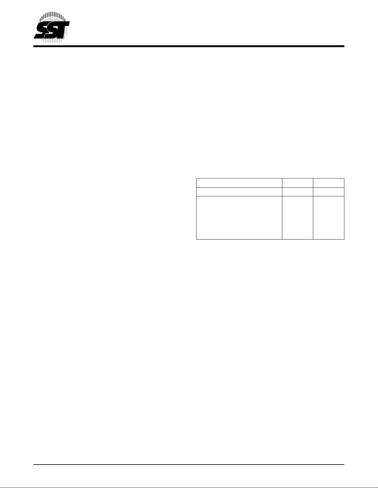
FUNCTIONAL BLOCK DIAGRAM OF THE SST27SF256
X-Decoder
A14 - A
0
Address Buffer
CE#
OE#
V
PP
A
9
Control Logic
FUNCTIONAL BLOCK DIAGRAM OF THE SST27SF512
X-Decoder
A15 - A
0
Address Buffer
SuperFlash
Memory
Y-Decoder
I/O Buffers
DQ7 - DQ
SuperFlash
Memory
Y-Decoder
0
502 ILL B1.1
CE#
OE#/V
PP
A
9
Control Logic
FUNCTIONAL BLOCK DIAGRAM OF THE SST27SF010/020
X-Decoder
A
- A
MS
0
CE#
OE#
A
9
V
PP
PGM#
AMS = A17 for SST27SF020, A16 for SST27SF010
Address Buffer
Control Logic
I/O Buffers
DQ7 - DQ
SuperFlash
Memory
Y-Decoder
I/O Buffers
DQ7 - DQ
0
502 ILL B2.1
0
502 ILL B3.2
©2001 Silicon Storage Technology, Inc. S71152-02-000 5/01 502
3
Page 4
A7
A6
A5
A4
A3
A2
A1
A0
DQ0
A7
A6
A5
A4
A3
A2
A1
A0
DQ0
256 Kbit / 512 Kbit / 1 Mbit / 2 Mbit Multi-Purpose Flash
SST27SF256 / SST27SF512 / SST27SF010 / SST27SF020
A12
A15
A16
VPPVDDPGM#
A12
A15
A16
VPPVDDPGM#
A7
A12
A15NCVDDA14
A7
A12
VPPNC
SST27SF256SST27SF512 SST27SF512SST27SF010 SST27SF010SST27SF020 SST27SF020SST27SF256
A6
A5
A4
A3
A2
A1
A0
NC
DQ0
A6
A5
A4
A3
A2
A1
A0
NC
DQ0
4 3 2 1 32 31 30
5
6
7
8
32-pin PLCC
9
10
11
12
13
T op Vie w
14 15 16 17 18 19 20
VDDA14
A17
NC
A13
A13
29
28
27
26
25
24
23
22
21
A8
A9
A11
NC
OE#
A10
CE#
DQ7
DQ6
A8
A9
A11
NC
OE#/V
A10
CE#
DQ7
DQ6
PP
A14
A13
A8
A9
A11
OE#
A10
CE#
DQ7
A14
A13
A8
A9
A11
OE#
A10
CE#
DQ7
Data Sheet
DQ1
SST27SF256SST27SF512 SST27SF512SST27SF010 SST27SF010SST27SF020 SST27SF020SST27SF256
DQ1
DQ1
DQ1
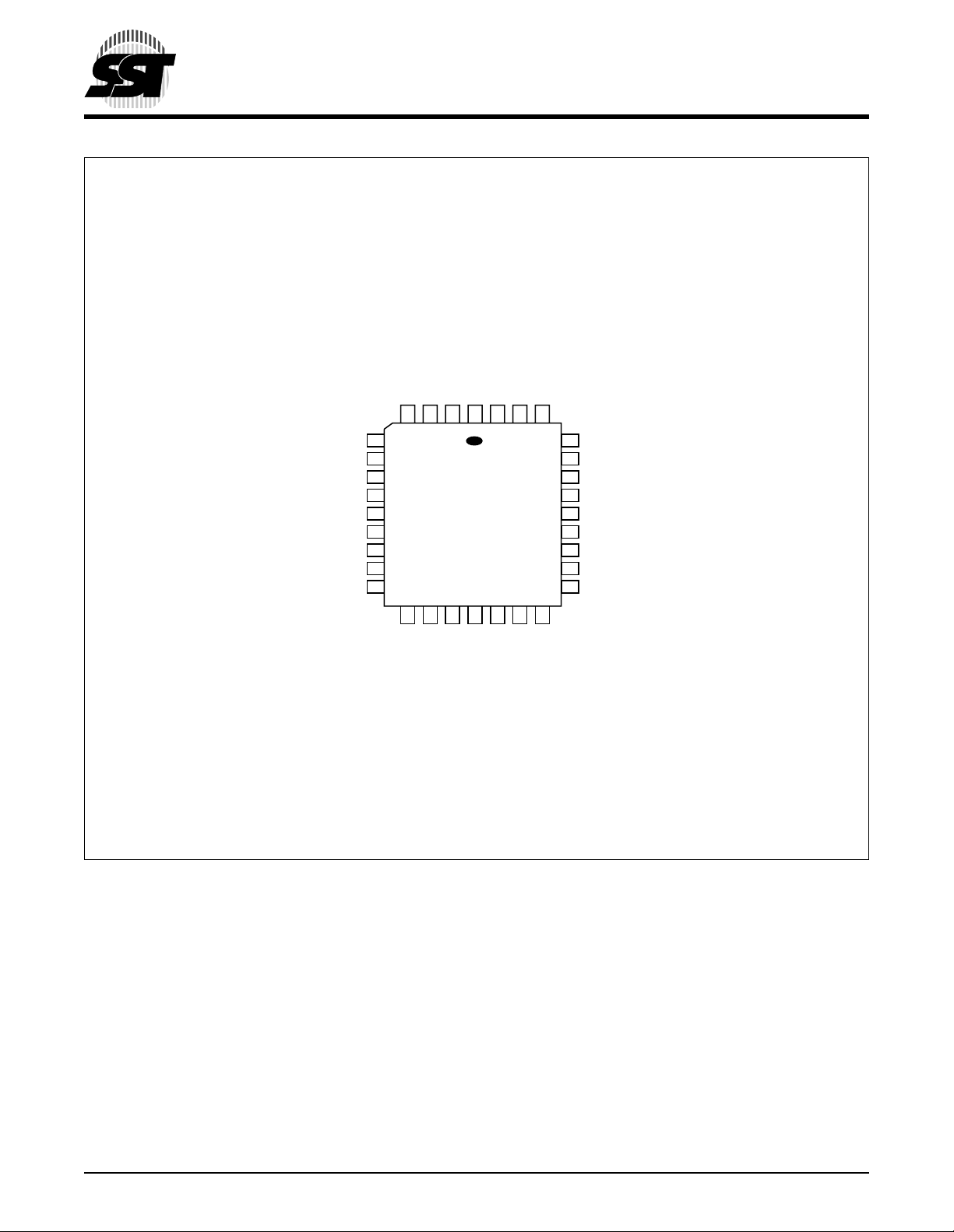
FIGURE 1: PIN ASSIGNMENTS FOR 32 -PIN PLCC
DQ2
DQ2
DQ2
DQ2
V
V
V
V
SS
SS
SS
SS
NC
NC
DQ3
DQ3
DQ3
DQ3
DQ4
DQ4
DQ4
DQ4
DQ5
DQ5
DQ5
DQ5
DQ6
DQ6
502 ILL F02c.2
©2001 Silicon Storage Technology, Inc. S71152-02-000 5/01 502
4
Page 5
256 Kbit / 512 Kbit / 1 Mbit / 2 Mbit Multi-Purpose Flash
SST27SF256 / SST27SF512 / SST27SF010 / SST27SF020
Data Sheet
SST27SF256SST27SF512 SST27SF512SST27SF010 SST27SF010SST27SF020 SST27SF020SST27SF256
A11
A9
A8
A13
A14
A17
PGM#
V
DD
V
PP
A16
A15
A12
A7
A6
A5
A4
FIGURE 2: PIN ASSIGNMENTS FOR 32 -PIN TSOP (8MM X 14MM)
A11
A13
A14
NC
PGM#
V
DD
V
PP
A16
A15
A12
V
A11
A13
A14
NC
NC
DD
NC
NC
A15
A12
A9
A8
A7
A6
A5
A4
A11
A9
A8
A7
A6
A5
A4
V
V
A13
A14
A12
NC
NC
DD
PP
NC
NC
A9
A8
A7
A6
A5
A4
1
2
3
4
5
6
7
8
9
10
11
12
13
14
15
16
Standard Pinout
T op Vie w
Die Up
OE#
32
A10
31
CE#
30
DQ7
29
DQ6
28
DQ5
27
DQ4
26
DQ3
25
V
24
DQ2
23
DQ1
22
DQ0
21
A0
20
A1
19
A2
18
A3
17
502 ILL F01.1
OE#/V
A10
CE#
DQ7
DQ6
DQ5
DQ4
DQ3
V
DQ2
DQ1
DQ0
A0
A1
A2
A3
SS
SS
OE#
PP
A10
CE#
DQ7
DQ6
DQ5
DQ4
DQ3
V
SS
DQ2
DQ1
DQ0
A0
A1
A2
A3
OE#
A10
CE#
DQ7
DQ6
DQ5
DQ4
DQ3
V
SS
DQ2
DQ1
DQ0
A0
A1
A2
A3
A7
A6
A5
A4
A3
A2
A1
A0
SS
V
PP
A12
A7
A6
A5
A4
A3
A2
A1
A0
DQ0
DQ1
DQ2
V
SS
A15
A12
DQ0
DQ1
DQ2
V
FIGURE 3: P
SST27SF512SST27SF256SST27SF512 SST27SF256
1
2
3
4
5
6
7
8
9
10
11
12
13
14
28-pin
PDIP
T op Vie w
28
27
26
25
24
23
22
21
20
19
18
17
16
15
V
DD
A14
A13
A8
A9
A11
OE#
A10
CE#
DQ7
DQ6
DQ5
DQ4
DQ3
502 ILL F02a.1
V
DD
A14
A13
A8
A9
A11
OE#/V
A10
CE#
DQ7
DQ6
DQ5
DQ4
DQ3
PP
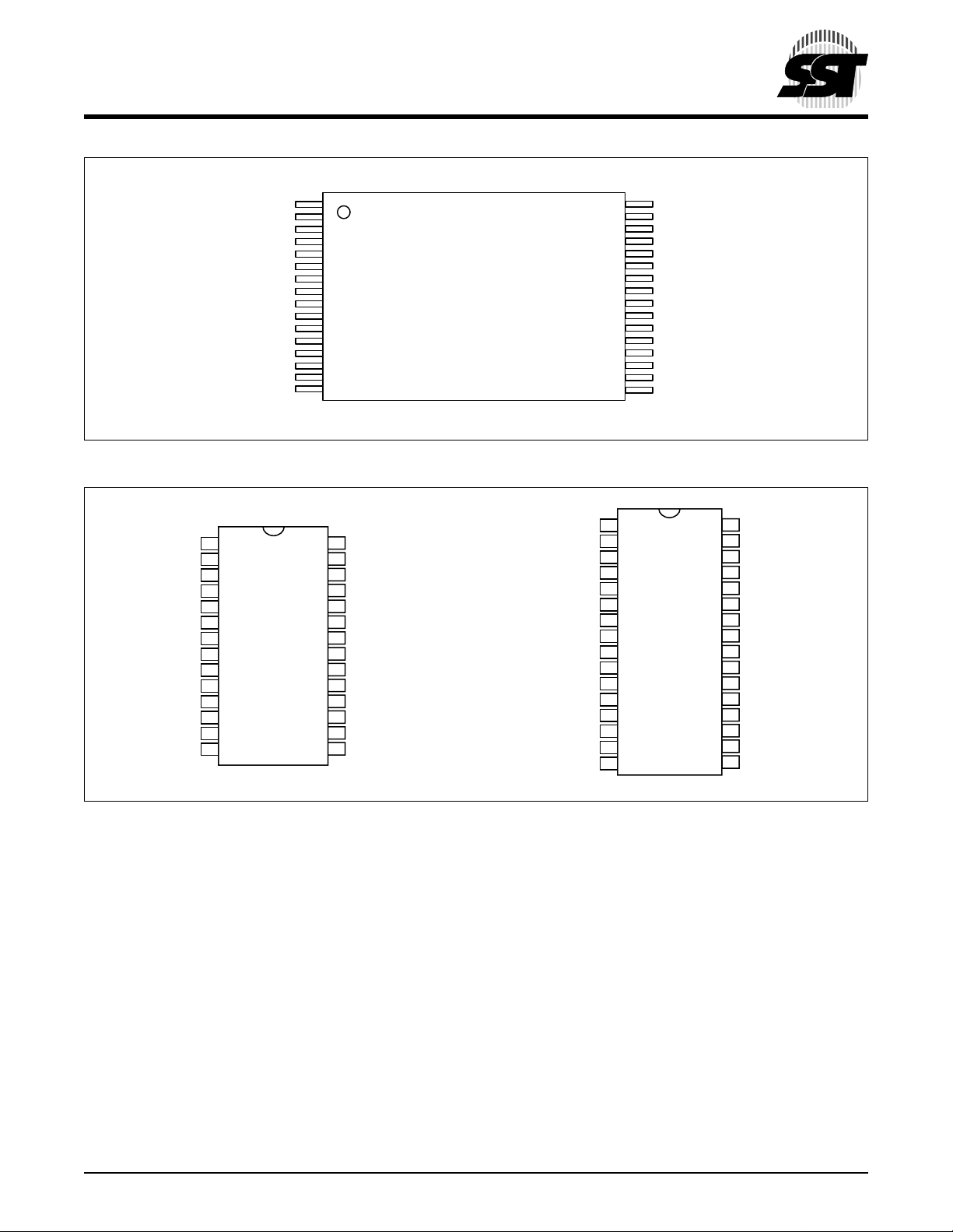
IN ASSIGNMEN TS FOR 28-PIN AND 32-PIN PDIP
SST27SF010 SST27SF010SST27SF020 SST27SF020
V
PP
A16
A15
A12
A7
A6
A5
A4
A3
A2
A1
A0
DQ0
DQ1
DQ2
V
SS
V
PP
A16
A15
A12
A7
A6
A5
A4
A3
A2
A1
A0
DQ0
DQ1
DQ2
V
SS
1
2
3
4
5
6
7
8
9
10
11
12
13
14
15
16
32-pin
PDIP
T op Vie w
32
31
30
29
28
27
26
25
24
23
22
21
20
19
18
17
502 ILL F02b.1
V
DD
PGM#
NC
A14
A13
A8
A9
A11
OE#
A10
CE#
DQ7
DQ6
DQ5
DQ4
DQ3
V
DD
PGM#
A17
A14
A13
A8
A9
A11
OE#
A10
CE#
DQ7
DQ6
DQ5
DQ4
DQ3
©2001 Silicon Storage Technology, Inc. S71152-02-000 5/01 502
5
Page 6
256 Kbit / 512 Kbit / 1 Mbit / 2 Mbit Multi-Purpose Flash
SST27SF256 / SST27SF512 / SST27SF010 / SST27SF020
TABLE 2: PIN DESCR IPTION
Symbol Pin Name Functions
1
-A
A
MS
DQ7-DQ
CE# Chip Enable To activate the device when CE# is low
OE# Output Enable For SST27SF256/010/020, to gate the data output buffers during Read operation
OE#/V
PP
V
PP
V
DD
V
SS
NC No Connection Unconnected pins.
1. AMS = Most significant address
A
MS
Address Inputs To provide memory addresses
0
Data Input/output To output data during Read cycles and receive input data during Program cycles
0
The outputs are in tri-state when OE# or CE# is high.
Output En able/VPPFor SST27SF512, to ga te the data ou tput b uff ers during Rea d opera tion and high v oltage
pin during Chip-Erase and programming operation
Power Supply for
Program or Erase
For SST27SF256/010/020, high voltage pin during Chip-Erase and programming opera-
tion 12V (±5%)
Power Supply To provide 5.0V supply (±10%)
Ground
= A14 for SST27SF256, A15 for SST27SF512, A16 for SST27SF010, and A17 for SST27SF020
Data Sheet
T2.3 502
©2001 Silicon Storage Technology, Inc. S71152-02-000 5/01 502
6
Page 7
256 Kbit / 512 Kbit / 1 Mbit / 2 Mbit Multi-Purpose Flash
SST27SF256 / SST27SF512 / SST27SF010 / SST27SF020
Data Sheet
TABLE 3: OPERATION MODES SELECTION FOR SST27SF256
Mode CE# OE# V
Read V
Output Disable V
Byte-Program V
Standby V
Chip-Erase V
Program/Erase Inhibit V
Product Identification V
Note: X = VIL or V
V
PPH
IH
= 12V±5%, VH = 12V±5%
IL
IL
IL
IH
IL
IH
IL
VILVDD or V
V
IHVDD
V
IHVPPH
XVDD or V
V
IHVPPH
XV
V
IL
PP
or V
PPH
VDD or V
TABLE 4: OPERATION MODES SELECTION FOR SST27SF512
Mode CE# OE#/V
Read V
Output Disable V
Program V
Standby V
Chip-Erase V
Program/Erase Inhibit V
Product Identification V
Note: X = V
or V
IL
V
PPH
IH
= 12V±5%, VH = 12V±5%
IL
IL
IL
IH
IL
IH
IL
PP
V
IL
V
IH
V
PPH
X X High Z X
V
PPH
V
PPH
V
IL
A9DQ Address
AIND
SS
SS
SS
OUT
XHigh Z X
AIND
IN
XHigh Z X
VHHigh Z X
XHigh Z X
VHManufacturer’s ID (BFH)
SS
Device ID (A3H)
A9DQ Address
AIND
OUT
X High Z X
AIND
IN
VHHigh Z X
X High Z X
VHManufacturer’s ID (BFH)
Device ID (A4H)
A
IN
A
IN
A14 - A1 = VIL, A0 = V
A14 - A1 = VIL, A0 = V
A
IN
A
IN
A15 - A1 = VIL, A0 = V
A15 - A1 = VIL, A0 = V
IL
IH
T3.1 502
IL
IH
T4.1 502
TABLE 5: OPERATION MODES SELECTION FOR SST27SF010/020
Mode CE# OE# PGM# A9V
Read V
Output Disable V
Program V
Standby V
Chip-Erase V
Program/Erase Inhibit V
Product Identification V
1. Device ID = A5H for SST27SF010 and A6H for SST27SF020
2. AMS = Most significant address
= A16 for SST27SF010 and A17 for SST27SF020
A
MS
Note: X = V
or V
IL
V
PPH
IH
= 12V±5%, VH = 12V±5%
V
IL
V
IL
V
IL
XXXVDD or V
IH
V
IL
XXXV
IH
V
IL
XAINVDD or V
IL
XXVDD or V
IH
V
IH
IH
IL
IL
V
IL
XVHVDD or V
AINV
VHV
PP
SSDOUT
SS
PPH
SS
PPH
PPH
SS
DQ Address
A
IN
High Z A
D
IN
IN
A
IN
High Z X
High Z X
High Z X
Manufacturer’s ID (BFH)
Device ID
1
2
A
- A1 = VIL, A0 = V
MS
2
A
- A1 = VIL, A0 = V
MS
IL
IH
T5.1 502
©2001 Silicon Storage Technology, Inc. S71152-02-000 5/01 502
7
Page 8
256 Kbit / 512 Kbit / 1 Mbit / 2 Mbit Multi-Purpose Flash
SST27SF256 / SST27SF512 / SST27SF010 / SST27SF020
Data Sheet
Absolute Maximum Stress Ratings (Applied conditions greater than those listed under “Absolute Maximum
Stress Ratings” may cause pe r manent dama ge to the device. This is a stres s rating only and funct ional operatio n
of the device at these conditions or conditions greater tha n those defined in the ope rational sections of this data
sheet is not implied. Exposure to absolute maximum stress rating conditions may affect device reliability.)
Temperature Under Bias . . . . . . . . . . . . . . . . . . . . . . . . . . . . . . . . . . . . . . . . . . . . . . . . . . . . . . . . . -55°C to +125°C
Storage Temperature . . . . . . . . . . . . . . . . . . . . . . . . . . . . . . . . . . . . . . . . . . . . . . . . . . . . . . . . . . . -65°C to +150°C
D. C. Voltage on Any Pin to Ground Potential . . . . . . . . . . . . . . . . . . . . . . . . . . . . . . . . . . . . . . . .-0.5V to V
Transient Voltage (<20 ns) on Any Pin to Ground Potential . . . . . . . . . . . . . . . . . . . . . . . . . . . . .-1.0V to V
Voltage on A
and VPP Pin to Ground Potential . . . . . . . . . . . . . . . . . . . . . . . . . . . . . . . . . . . . . . . . . -0.5V to 14.0V
9
Package Power Dissipation Capability (Ta = 25°C) . . . . . . . . . . . . . . . . . . . . . . . . . . . . . . . . . . . . . . . . . . . . . . 1.0W
Through Hold Lead Soldering Temperature (10 Seconds) . . . . . . . . . . . . . . . . . . . . . . . . . . . . . . . . . . . . . . . 300°C
Surface Mount Lead Soldering Temperature (3 Seconds) . . . . . . . . . . . . . . . . . . . . . . . . . . . . . . . . . . . . . . . 240°C
1
Output Short Circ uit Curr ent
1. Outputs shorted for no more than one second. No more than one output shorted at a time.
. . . . . . . . . . . . . . . . . . . . . . . . . . . . . . . . . . . . . . . . . . . . . . . . . . . . . . . . . . . . 100 mA
DD
DD
+0.5V
+1.0V
OPERATING RANGE
Range Ambient Temp V
DD
Commercial 0°C to +70°C5.0V±10%12V±5%
V
PP
AC CONDITIONS OF TEST
Input Rise/Fall Time . . . . . . . . . . . 10 ns
Output Load . . . . . . . . . . . . . . . . . C
Output Load . . . . . . . . . . . . . . . . . C
See Figures 11 and 12
TABLE 6: READ MODE DC OPERATING CHARACTERISTICS FOR SST27SF256/512/010/020
= 5.0V±10%, VPP=VDD OR V
V
DD
Symbol Parameter
I
DD
I
PPR
I
SB1
VDD Read Current Address input=VIL/VIH at f=1/TRC Min
VPP Read Current Address input=VIL/VIH at f=1/TRC Min
Standby VDD Current
(TTL input)
I
SB2
Standby VDD Current
(CMOS input)
I
LI
I
LO
V
IL
V
IH
V
OL
V
OH
I
H
Input Leakage Current 1 µA VIN=GND to VDD, VDD=VDD Max
Output Leakage Current 10 µA V
Input Low Voltage 0.8 V VDD=VDD Min
Input High Voltage 2.0 VDD+0.5 V VDD=VDD Max
Output Low Voltage 0.2 V IOL=2.1 mA, VDD=VDD Min
Output High Voltage 2.4 V IOH=-400 µA, VDD=VDD Min
Supervoltage Current for A
9
(Ta = 0°C to +70°C (Commercial))
SS
Limits
30 mA CE#=OE#=V
100 µA CE#=OE#=VIL, all I/Os open
3mACE#=V
100 µA CE#=VDD-0.3
100 µA CE#=OE#=VIL, A9=VH Max
Test ConditionsMin Max Units
V
DD=VDD
V
DD=VDD
V
DD=VDD
OUT
Max
, all I/Os open
IL
Max, VPP=V
, VDD=VDD Max
IH
Max
=GND to VDD, VDD=VDD Max
= 100 pF for 90 ns
L
= 30 pF for 70 ns
L
DD
T6.3 502
©2001 Silicon Storage Technology, Inc. S71152-02-000 5/01 502
8
Page 9

256 Kbit / 512 Kbit / 1 Mbit / 2 Mbit Multi-Purpose Flash
SST27SF256 / SST27SF512 / SST27SF010 / SST27SF020
Data Sheet
TABLE 7: PROGRAM/ERASE DC OPERATING CHARACTERISTICS FOR S ST27S F256
=5.0V±10%, VPP=V
V
DD
Symbol Parameter
I
I
I
I
V
I
V
DD
PP
LI
LO
H
H
PPH
VDD Erase or Program Current 30 mA CE#=V
VPP Erase or Program Current 1 mA CE#=V
Input Leakage Current 1 µA VIN=GND to VDD, VDD=VDD Max
Output Leakage Current 1 µA V
Supervol tage for A
9
Supervol tage Curre nt for A
High Voltage for VPP Pin 11.4 12.6 V
TABLE 8: PROGRAM/ERASE DC OPERATING CHARACTERISTICS FOR S ST27S F512
=5.0V±10%, VPP=V
V
DD
Symbol Parameter
I
I
I
I
V
I
V
DD
PP
LI
LO
H
H
PPH
VDD Erase or Program Current 30 mA CE#=V
VPP Erase or Program Current 1 mA CE#=V
Input Leakage Current 1 µA VIN=GND to VDD, VDD=VDD Max
Output Leakage Current 1 µA V
Supervol tage for A
9
Supervol tage Curre nt for A
High Voltage for OE#/VPP Pin 11.4 12.6 V
PPH
9
PPH
9
(Ta=25°C±5°C)
Limits
Test ConditionsMin Max Units
=GND to VDD, VDD=VDD Max
OUT
11.4 12.6 V CE#=OE#=V
100 µA CE#=OE#=V
(Ta=25°C±5°C)
Limits
Test ConditionsMin Max Units
=GND to VDD, VDD=VDD Max
OUT
11.4 12.6 V CE#=OE#/VPP=V
100 µA CE#=OE#/VPP=V
OE#=VIH, VPP=12V±5%, VDD=VDD Max
IL,
OE#=VIH, VPP=12V±5%, VDD=VDD Max
IL,
IL,
IL, A9=VH
OE#/VPP=12V±5%, VDD=VDD Max
IL,
OE#/VPP=12V±5%, VDD=VDD Max
IL,
Max
IL,
IL, A9=VH
T7.1 502
Max
T8.1 502
TABLE 9: PROGRAM/ERASE DC OPERATING CHARACTERISTICS FOR S ST27S F010/020
=5.0V±10%, VPP=V
V
DD
Symbol Parameter
I
I
I
I
V
I
V
DD
PP
LI
LO
H
H
PPH
VDD Erase or Program Current 30 mA CE#=PGM#=V
VPP Erase or Program Current 1 mA CE#=PGM#=V
Input Leakage Current 1 µA VIN =GND to VDD, VDD=VDD Max
Output Leakage Current 1 µA V
Supervol tage for A
Supervol tage Curre nt for A
High Voltage for VPP Pin 11.4 12.6 V
9
PPH
9
(Ta=25°C±5°C)
Limits
Test ConditionsMin Max Units
V
V
11.4 12.6 V CE#=OE#=V
100 µA CE#=OE#=V
OE#=VIH, VPP=12V±5%,
IL,
DD=VDD
DD=VDD
OUT
Max
OE#=VIH, VPP=12V±5%,
IL,
Max
=GND to VDD, VDD=VDD Max
IL,
IL, A9=VH
Max
T9.1 502
©2001 Silicon Storage Technology, Inc. S71152-02-000 5/01 502
9
Page 10

256 Kbit / 512 Kbit / 1 Mbit / 2 Mbit Multi-Purpose Flash
SST27SF256 / SST27SF512 / SST27SF010 / SST27SF020
Data Sheet
TABLE 10: RECOMMENDED S YSTEM POWER-UP TIMINGS
Symbol Parameter Minimum Units
T
T
1
PU-READ
PU-WRITE
1
1. This parameter is measured only for initial qualification and after a design or process change that could affect this parameter.
TABLE 11: CAPACITANCE (Ta = 25°C, f= 1 Mhz, other pins open)
Parameter Description Test Condition Maximum
1
C
I/O
1
C
IN
1. This parameter is measured only for initial qualification and after a design or process change that could affect this parameter.
TABLE 12: RELIABILITY CHARACTERISTICS
Symbol Parameter Minimum Specification Units Test Method
1
N
END
1
T
DR
1
I
LTH
1. This parameter is measured only for initial qualification and after a design or process change that could affect this parameter.
Power-up to Read Operation 100 µs
Power-up to Write Operation 100 µs
I/O Pin Capacitance V
= 0V 12 pF
I/O
Input Capacitance VIN = 0V 6 pF
Endurance 1000 Cycles JEDEC Standard A117
Data Retention 100 Years JEDEC Standard A103
Latch Up 100 mA JEDEC Standard 78
T10.1 502
T11.0 502
T12.2 502
AC CHARACTERISTICS
TABLE 13: READ CYCLE TIMING PARAMETER S VDD = 5.0V±10% (Ta = 0°C to +70°C (Commercial))
SST27SF256-70
SST27SF512-70
SST27SF010-70
SST27SF020-70
Symbol Parameter
T
RC
T
CE
T
AA
T
OE
1
T
CLZ
1
T
OLZ
1
T
CHZ
1
T
OHZ
1
T
OH
1. This parameter is measured only for initial qualification and after a design or process change that could affect this parameter.
Read Cycle Time 70 90 ns
Chip Enable Access Time 70 90 ns
Address Acce ss Time 70 90 ns
Output Enable Access Time 35 45 ns
CE# Low to Active Output 0 0 ns
OE# Low to Active Output 0 0 ns
CE# High to High-Z Output 25 30 ns
OE# High to High-Z Output 25 30 ns
Output Hold from Address Change 0 0 ns
SST27SF256-90
SST27SF512-90
SST27SF010-90
SST27SF020-90
UnitsMinMaxMinMax
T13.1 502
©2001 Silicon Storage Technology, Inc. S71152-02-000 5/01 502
10
Page 11

256 Kbit / 512 Kbit / 1 Mbit / 2 Mbit Multi-Purpose Flash
SST27SF256 / SST27SF512 / SST27SF010 / SST27SF020
Data Sheet
TABLE 14: PROGRAM/ERASE CYCLE TIMING PARAMETERS FOR SST27SF256
Symbol Parameter Min Max Units
T
AS
T
AH
T
PRT
T
VPS
T
VPH
T
PW
T
EW
T
DS
T
DH
T
VR
T
ART
T
A9S
T
A9H
TABLE 15: PROGRAM/ERASE CYCLE TIMING PARAMETERS FOR SST27SF512
Symbol Parameter Min Max Units
T
AS
T
AH
T
PRT
T
VPS
T
VPH
T
PW
T
EW
T
DS
T
DH
T
VR
T
ART
T
A9S
T
A9H
TABLE 16: PROGRAM/ERASE CYCLE TIMING PARAMETERS FOR SST27SF010/020
Symbol Parameter Min Max Units
T
CES
T
CEH
T
AS
T
AH
T
PRT
T
VPS
T
VPH
T
PW
T
EW
T
DS
T
DH
T
VR
T
ART
T
A9S
T
A9H
Address Setup Time 1 µs
Address Hold Time 1 µs
VPP Pulse Rise Time 50 ns
VPP Setup Time 1 µs
VPP Hold Time 1 µs
CE# Program P ulse Width 20 30 µs
CE# Erase Pulse Width 100 500 ms
Data Setup Time 1 µs
Data Hold Time 1 µs
VPP and A9 Recovery Time 1 µs
A9 Rise Time to 12V during Erase 50 ns
A9 Setup Time during Erase 1 µs
A9 Hold Time during Erase 1 µs
Address Setup Time 1 µs
Address Hold Time 1 µs
OE#/VPP Pulse Rise Time 50 ns
OE#/VPP Setup Time 1 µs
OE#/VPP Hold Time 1 µs
CE# Program P ulse Width 20 30 µs
CE# Erase Pulse Width 100 500 ms
Data Setup Time 1 µs
Data Hold Time 1 µs
OE#/VPP and A9 Recovery Time 1 µs
A9 Rise Time to 12V during Erase 50 ns
A9 Setup Time during Erase 1 µs
A9 Hold Time during Erase 1 µs
CE# Setup Time 1 µs
CE# Hold Time 1 µs
Address Setup Time 1 µs
Address Hold Time 1 µs
VPP Pulse Rise Time 50 ns
VPP Setup Time 1 µs
VPP Hold Time 1 µs
PGM# Program Pulse Width 20 30 µs
PGM# Erase Pulse Width 100 500 ms
Data Setup Time 1 µs
Data Hold Time 1 µs
A9 Recovery Time for Erase 1 µs
A9 Rise Time to 12V during Erase 50 ns
A9 Setup Time during Erase 1 µs
A9 Hold Time during Erase 1 µs
T14.0 502
T15.0 502
T16.0 502
©2001 Silicon Storage Technology, Inc. S71152-02-000 5/01 502
11
Page 12

256 Kbit / 512 Kbit / 1 Mbit / 2 Mbit Multi-Purpose Flash
SST27SF256 / SST27SF512 / SST27SF010 / SST27SF020
Data Sheet
T
RC
T
AA
ADDRESS
T
T
T
CLZ
OLZ
CE
T
OE
T
OH
DQ
CE#
OE#
7-0
HIGH-Z
FIGURE 4: READ CYCLE TIMING DIA GRAM FOR SST27SF256/512/010/020
ADDRESS
(EXCEPT A9)
T
OHZ
T
CHZ
DATA VALIDDATA VALID
502 ILL F03.0
CE#
T
EW
OE#
V
IH
DQ
7-0
V
PPH
V
DD
V
PP
V
SS
V
PPH
A
9
V
IH
V
IL
FIGURE 5: C
©2001 Silicon Storage Technology, Inc. S71152-02-000 5/01 502
HIP-ERASE TIMING DIAGRAM FOR SST27SF256
T
T
PRT
ART
T
T
A9S
VPS
T
T
VPH
A9H
T
VR
T
VR
502 ILL F04a.1
12
Page 13

256 Kbit / 512 Kbit / 1 Mbit / 2 Mbit Multi-Purpose Flash
SST27SF256 / SST27SF512 / SST27SF010 / SST27SF020
Data Sheet
ADDRESS
(EXCEPT A9)
CE#
T
EW
DQ
7-0
V
OE#/V
PP
A
PPH
V
DD
V
SS
V
PPH
9
V
IH
V
IL
T
T
PRT
ART
T
T
VPS
A9S
T
T
VPH
A9H
T
VR
T
VR
502 ILL F04b.1
FIGURE 6: READ CYCLE TIMING DIA GRAM FOR SST27SF512
ADDRESS
(EXCEPT A9)
CE#
OE#
V
IH
DQ
7-0
V
V
PP
A
PGM#
PPH
V
DD
V
SS
V
PPH
9
V
V
T
IH
IL
PRT
T
ART
T
T
T
VPS
A9S
CES
T
EW
T
T
T
CEH
VPH
A9H
T
VR
502 ILL F04c.1
FIGURE 7: C
©2001 Silicon Storage Technology, Inc. S71152-02-000 5/01 502
HIP-ERASE TIMING DIAGRAM FOR SST27SF010/020
13
Page 14

256 Kbit / 512 Kbit / 1 Mbit / 2 Mbit Multi-Purpose Flash
SST27SF256 / SST27SF512 / SST27SF010 / SST27SF020
Data Sheet
ADDRESS
ADDRESS VALID
T
AS
T
AH
CE#
OE#
DQ
V
7-0
PP
V
IH
HIGH-Z
V
PPH
V
DD
V
SS
T
PRT
DATA VALID
T
VPS
FIGURE 8: BYTE-PROGRAM TIMING DIAGRAM FOR SST27SF256
T
PW
T
DS
T
VPH
T
DH
T
VR
502 ILL F05a.1
ADDRESS
DQ
OE#/V
FIGURE 9: B
ADDRESS VALID
T
AS
T
AH
CE#
7-0
PP
HIGH-Z
V
PPH
V
DD
V
SS
T
PRT
DATA VALID
T
VPS
YTE-PROGRAM TIMING DIAGRAM FOR SST27SF512
T
PW
T
DS
T
VPH
T
DH
T
VR
502 ILL F05b.2
©2001 Silicon Storage Technology, Inc. S71152-02-000 5/01 502
14
Page 15

256 Kbit / 512 Kbit / 1 Mbit / 2 Mbit Multi-Purpose Flash
SST27SF256 / SST27SF512 / SST27SF010 / SST27SF020
Data Sheet
ADDRESS
CE#
OE#
DQ
7-0
V
PP
V
IH
HIGH-Z
V
PPH
V
DD
V
SS
ADDRESS VALID
DATA VALID
T
VPS
T
PRT
T
AS
T
DS
PGM#
T
CES
FIGURE 10: BYTE-PROGRAM TIMING DIAGRAM FOR SST 27SF010/020
T
AH
T
CEH
T
DH
T
PW
T
VPH
502 ILL F05c.1
©2001 Silicon Storage Technology, Inc. S71152-02-000 5/01 502
15
Page 16

256 Kbit / 512 Kbit / 1 Mbit / 2 Mbit Multi-Purpose Flash
SST27SF256 / SST27SF512 / SST27SF010 / SST27SF020
Data Sheet
V
IHT
V
ILT
V
HT
REFERENCE POINTS OUTPUTINPUT
V
LT
V
HT
V
LT
502 ILL F06.0
AC test inputs are driven at V
inputs and outputs are V
HT
(2.4 V) for a logic “1” and V
IHT
(2.0 V) and VLT (0.8 V). Input rise and fall times (10% ↔ 90%) are <10 ns.
FIGURE 11: AC INPUT/OUTPUT REFERENCE WAVEFORMS
TO TESTER
TO DUT
C
L
(0.4 V) for a logic “0”. M eas ure me nt r eference poi nt s for
IL T
R
L LOW
V
DD
Note: V
R
L HIGH
- V
- V
- V
- V
HIGH
LOW
INPUT
INPUT
Test
Test
HIGH Test
LOW Test
HT
V
LT
V
IHT
V
ILT
502 ILL F07.1
FIGURE 12: A TEST LOAD EXAMPLE
©2001 Silicon Storage Technology, Inc. S71152-02-000 5/01 502
16
Page 17

256 Kbit / 512 Kbit / 1 Mbit / 2 Mbit Multi-Purpose Flash
SST27SF256 / SST27SF512 / SST27SF010 / SST27SF020
Data Sheet
Start
VPP = V
Yes
PPH, A9
Erase 100ms pulse
(CE# = VIL)
VPP = VDD or V
A9 = VIL or V
Wait for VPP and A9
Recovery Time
Read Device
(CE# = OE# = VIL)
Compare All
bytes to FFH
Device Passed
= V
SS
IH
H
No
Device Failed
502 ILL F08a.2
FIGURE 13: CHIP-ERASE ALGORITHM FOR SST27SF256
©2001 Silicon Storage Technology, Inc. S71152-02-000 5/01 502
17
Page 18

256 Kbit / 512 Kbit / 1 Mbit / 2 Mbit Multi-Purpose Flash
SST27SF256 / SST27SF512 / SST27SF010 / SST27SF020
Data Sheet
Start
A9 = V
H
OE#/VPP = V
Erase 100ms pulse
(CE# = VIL)
OE#/VPP = VDD or V
A9 = VIL or V
Wait for OE#/VPP and
A9 Recovery Time
Read Device
(CE# = OE# = VIL)
Compare All
bytes to FFH
Yes
Device Passed
PPH
IH
SS
No
Device Failed
502 ILL F08b.2
FIGURE 14: CHIP-ERASE ALGORITHM FOR SST27SF512
©2001 Silicon Storage Technology, Inc. S71152-02-000 5/01 502
18
Page 19

256 Kbit / 512 Kbit / 1 Mbit / 2 Mbit Multi-Purpose Flash
SST27SF256 / SST27SF512 / SST27SF010 / SST27SF020
Data Sheet
Start
A9 = VH, VPP = V
CE# = VIL, OE# = V
Erase 100ms pulse
(PGM# = VIL)
PGM# = V
A9 = VIL or V
Wait A9 Recovery Time
Read Device
Compare all
bytes to FFH
PPH
IH
IH
IH
No
Yes
Device Passed
FIGURE 15: CHIP-ERASE ALGORITHM FOR SST27SF010/020
Device Failed
502 ILL F08c.1
©2001 Silicon Storage Technology, Inc. S71152-02-000 5/01 502
19
Page 20

256 Kbit / 512 Kbit / 1 Mbit / 2 Mbit Multi-Purpose Flash
SST27SF256 / SST27SF512 / SST27SF010 / SST27SF020
Data Sheet
Start
Erase*
VPP = V
PPH
Address = First Location
Program 20µs pulse
(CE# = VIL)
Increment Address
* See Figure 13
No
Last Address?
Yes
Yes
FIGURE 16: BYTE-PROGRAM ALGORITHM FOR SST27SF256
VPP = VDD or V
Wait for VPP
RecoveryTime
Read Device
(CE# = OE# = VIL)
Compare all bytes
to original data
Device Passed
SS
No
Device Failed
502 ILL F09a.3
©2001 Silicon Storage Technology, Inc. S71152-02-000 5/01 502
20
Page 21

256 Kbit / 512 Kbit / 1 Mbit / 2 Mbit Multi-Purpose Flash
SST27SF256 / SST27SF512 / SST27SF010 / SST27SF020
Data Sheet
Start
Erase*
Increment Address
OE#/VPP = V
Address = First Location
Program 20µs pulse
(CE# = VIL)
Last Address?
No
PPH
Yes
OE#/VPP = VDD or V
Wait for OE#/VPP
RecoveryTime
Read Device
(CE# = OE# = VIL)
Compare all bytes
to original data
Yes
SS
No
Device Passed
* See Figure 14
Device Failed
502 ILL F09b.2
FIGURE 17: BYTE-PROGRAM ALGORITHM FOR SST27SF512
©2001 Silicon Storage Technology, Inc. S71152-02-000 5/01 502
21
Page 22

256 Kbit / 512 Kbit / 1 Mbit / 2 Mbit Multi-Purpose Flash
SST27SF256 / SST27SF512 / SST27SF010 / SST27SF020
Data Sheet
Start
Erase*
Increment Address
VPP = V
Address = First Location
CE# = VIL, OE# = V
Program 20µs pulse
(PGM# = VIL)
Last Address?
No
PPH
IH
Yes
Read Device
Compare all bytes
to original data
No
Yes
Device Passed
* See Figure 15
Device Failed
502 ILL F09c.1
FIGURE 18: BYTE-PROGRAM ALGORITHM FOR SST27SF010/020
©2001 Silicon Storage Technology, Inc. S71152-02-000 5/01 502
22
Page 23

256 Kbit / 512 Kbit / 1 Mbit / 2 Mbit Multi-Purpose Flash
SST27SF256 / SST27SF512 / SST27SF010 / SST27SF020
Data Sheet
Device Speed Suffix1 Suffix2
SST27SFxxx
-XXX -XX -XX
Package Modifi e r
G = 28 pins
H = 32 pins
Numeric = Die modifier
Package Type
N = PLCC
W = TSOP (die up) (8mm x 14mm)
P = PDIP
Operating Temperature
C = Commercial = 0° to +70°C
Minimum Endurance
3 = 1000 cycles
Read Access Speed
70 = 70 ns
90 = 90 ns
Device Density
256 = 256 Kilobit
512 = 512 Kilobit
010 = 1 Megabit
020 = 2 Megabit
©2001 Silicon Storage Technology, Inc. S71152-02-000 5/01 502
23
Page 24

256 Kbit / 512 Kbit / 1 Mbit / 2 Mbit Multi-Purpose Flash
SST27SF256 / SST27SF512 / SST27SF010 / SST27SF020
Valid combinations for SST27SF256
SST27SF256-70-3C-NH SST27SF256-70-3C-WH SST27SF256-70-3C-PG
SST27SF256-90-3C-NH SST27SF256-90-3C-WH SST27SF256-90-3C-PG
Valid combinations for SST27SF512
SST27SF512-70-3C-NH SST27SF512-70-3C-WH SST27SF512-70-3C-PG
SST27SF512-90-3C-NH SST27SF512-90-3C-WH SST27SF512-90-3C-PG
Valid combinations for SST27SF010
SST27SF010-70-3C-NH SST27SF010-70-3C-WH SST27SF010-70-3C-PH
SST27SF010-90-3C-NH SST27SF010-90-3C-WH SST27SF010-90-3C-PH
Valid combinations for SST27SF020
SST27SF020-70-3C-NH SST27SF020-70-3C-WH SST27SF020-70-3C-PH
SST27SF020-90-3C-NH SST27SF020-90-3C-WH SST27SF020-90-3C-PH
Data Sheet
Example: Valid combinations are those products in mass production or will be in mass production. Consult your SST sales
representative to confirm availability of valid combinations and to determine availability of new combinations.
©2001 Silicon Storage Technology, Inc. S71152-02-000 5/01 502
24
Page 25

256 Kbit / 512 Kbit / 1 Mbit / 2 Mbit Multi-Purpose Flash
SST27SF256 / SST27SF512 / SST27SF010 / SST27SF020
Data Sheet
PACKAGING DIAGRAMS
TOP VIEW SIDE VIEW BO TT OM VIEW
.485
Optional
Pin #1 Identifier
.042
.048
.495
.447
.453
1232
.020 R.
MAX.
.023
.029
x 30˚
.106
.112
.030
.040
R.
.042
.048
.547
.585
.553
.595
.050
BSC.
Note: 1. Complies with JEDEC publication 95 MS-016 AE dimensions, although some dimensions may be more stringent.
2. All linear dimensions are in inches (min/max).
3. Dimensions do not include mold flash. Maximum allowable mold flash is .008 inches.
4. Coplanarity: 4 mils.
32-PIN PLASTIC LEAD CHIP CARRIER (PLCC)
ACKAGE CODE: NH
SST P
Pin # 1 Identifier
.026
.032
.050
BSC.
.125
.140
.075
.095
.013
.021
8.10
7.90
.400
BSC
.015 Min.
1.05
0.95
.490
.530
.50
BSC
.270
.170
.026
.032
32.PLCC.NH-ILL.2
12.50
12.30
0.70
0.50
Note: 1. Complies with JEDEC publication 95 MO-142 BA dimensions, although some dimensions may be more stringent.
2. All linear dimensions are in millimeters (min/max).
3. Coplanarity: 0.1 (±.05) mm.
4. Maximum allowable mold flash is 0.15mm at the package ends, and 0.25mm between leads.
32-
PIN THIN SMALL OUTLINE PACKAGE (TSOP) 8MM X 14MM
14.20
13.80
32.TSOP-WH-ILL.4
0.15
0.05
SST PACKAGE CODE: WH
©2001 Silicon Storage Technology, Inc. S71152-02-000 5/01 502
25
Page 26

Pin #1 Identifier
.065
.075
256 Kbit / 512 Kbit / 1 Mbit / 2 Mbit Multi-Purpose Flash
SST27SF256 / SST27SF512 / SST27SF010 / SST27SF020
Data Sheet
28
C
L
.600
1
1.445
1.455
7˚
4 PLCS.
.625
.530
.550
Base Plane
Seating Plane
.015
.050
.070
.080
Note: 1. Complies with JEDEC publication 95 MO-015 AH dimensions, although some dimensions may be more stringent.
2. All linear dimensions are in inches (min/max).
3. Dimensions do not include mold flash. Maximum allowable mold flash is .010 inches.
.045
.065
28-PIN PLASTIC DUAL-IN-LINE PAC KA GE (PDIP)
ACKAGE CODE: PG
SST P
32
C
L
Pin #1 Identifier
.065
.075
1
1.645
1.655
.016
.022
.100 BSC
.120
.150
.170
.200
.008
.012
4 PLCS.
0˚
15˚
.600 BSC
28.pdipPG-ILL.2
.600
.625
.530
7˚
.550
.120
.150
.170
.200
.008
.012
.600 BSC
32.pdipPH-ILL.2
0˚
15˚
Base Plane
Seating Plane
.015
.050
.070
.080
Note: 1. Complies with JEDEC publication 95 MO-015 AP dimensions, although some dimensions may be more stringent.
32-
PIN PLASTIC DUAL-IN-LINE PACKAGE (PDIP)
ACKAGE CODE: PH
SST P
2. All linear dimensions are in inches (min/max).
3. Dimensions do not include mold flash. Maximum allowable mold flash is .010 inches.
.045
.065
.016
.022
.100 BSC
Silicon Storage Technology, Inc. • 1171 Sonora Court • Sunnyvale, CA 940 86 • Telephone 408-735-9110 • Fax 408-735-9036
www.SuperFlash.com or www.ssti.com
©2001 Silicon Storage Technology, Inc. S71152-02-000 5/01 502
26
 Loading...