

Page 1

Stereo Audio Amplifier
SSM3302
Rev. 0
Information furnished by Analog Devices is believed to be accurate and reliable. However, no
Trademarks and registered trademarks are the property of their respective owners.
Fax: 781.461.3113 ©2012 Analog Devices, Inc. All rights reserved.
Data Sheet
FEATURES
Filterless stereo Class-D amplifier with Σ-Δ modulation
2 × 10 W into 4 Ω load and 2 × 8 W into 8 Ω load at 12 V supply
with <1% total harmonic distortion plus noise (THD + N)
91% efficiency at 12 V, 8 W into 8 Ω speaker
98 dB signal-to-noise ratio (SNR)
Single-supply operation from 7 V to 18 V
Flexible gain adjustment pin from 9 dB to 24 dB
Fixed input impedance of 40 kΩ
Mono output mode pin for 1 × 20 W output power into 2 Ω
10 µA shutdown current
Short-circuit and thermal protection
Available in a 40-lead, 6 mm × 6 mm LFCSP
Pop-and-click suppression
User-selectable ultralow EMI emissions mode
Thermal warning indicator
Power-on reset
APPLICATIONS
Mobile computing
Flat panel televisions
Media docking stations
Portable electronics
Sound bars
GENERAL DESCRIPTION
The SSM3302 is a fully integrated, high efficiency, stereo Class-D
audio amplifier. The application circuit requires minimal external
components and operates from a single 7 V to 18 V supply. The
device is capable of delivering 2 × 10 W of continuous output
power into a 4 Ω load (or 2 × 8 W into 8 Ω) with <1% THD + N
from a 12 V supply. In addition, while mono mode is activated,
the user can drive a load as small as 2 Ω up to 20 W continuous
output power by stacking the stereo output terminals.
The SSM3302 features a high efficiency, low noise modulation
scheme that requires no external LC output filters. This scheme
continues to provide high efficiency even at low output power.
The SSM3302 operates with 90% efficiency at 7 W into an 8 Ω
2 ×10 W Filterless Class-D
load or with 82% efficiency at 10 W into 4 Ω from a 12 V supply,
and it has an SNR of >98 dB.
Spread spectrum pulse density modulation (PDM) is used to
provide lower EMI radiated emissions compared with other
Class-D architectures. The SSM3302 includes an optional
modulation select pin (ultralow EMI emission mode) that
significantly reduces the radiated emissions at the Class-D
outputs, particularly above 100 MHz. The SSM3302 can pass
FCC Class-B emissions testing with an unshielded 20 inch cable
using common-mode choke-based filtering.
The fully differential input of the S
rejection of common-mode noise on the input. The device also
includes a highly flexible gain select pin that only requires one
series resistor to choose a gain between 9 dB and 24 dB, with no
change to the input impedance. The benefit of this is to improve
gain matching between multiple SSM3302 devices within a single
application compared with using external resistors to set gain.
The SSM3302 includes an integrated voltage regulator that
generates a 5 V rail.
The SSM3302 has a micropower shutdown mode with a typical
shutdown current of 10 µA. Shutdown is enabled by applying a
logic low to the
suppression circuitry that minimizes voltage glitches at the output
during turn on and turn off, reducing audible noise during
activation and deactivation.
Other included features to simplify system level integration of
the SSM3302 are input low-pass filtering to suppress out-ofband DAC noise interference to the pulse density modulator,
fixed input impedance to simplify component selection across
multiple platform production builds, and a thermal warning
indicator pin.
The SSM3302 is specified over the commercial temperature
range (−40°C to +85°C). It has built-in thermal shutdown and
output short-circuit protection. It is available in a halide-free,
40-lead, 6 mm × 6 mm lead frame chip scale package (LFCSP).
SD
pin. The device also includes pop-and-click
SM3302 provides excellent
responsibility is assumed by Analog Devices for its use, nor for any infringements of patents or other
rights of thi rd parties that may result from its use. Specifications subject to change with out notice. No
license is granted by implication or otherwise under any patent or patent rights of Analog Devices.
One Technology Way, P.O. Box 9106, Norwood, MA 02062-9106, U.S.A.
Tel: 781.329.4700
www.analog.com
Page 2

SSM3302 Data Sheet
TABLE OF CONTENTS
Features.............................................................................................. 1
Applications....................................................................................... 1
General Description ......................................................................... 1
Revision History ............................................................................... 2
Functional Block Diagram .............................................................. 3
Specifications..................................................................................... 4
Absolute Maximum Ratings............................................................ 6
Thermal Resistance ...................................................................... 6
ESD Caution.................................................................................. 6
Pin Configuration and Function Descriptions............................. 7
Typical Performance Characteristics ............................................. 8
Typical Application Circuits.......................................................... 14
Applications Information .............................................................. 16
Overview...................................................................................... 16
Analog Supply............................................................................. 16
Gain Selection............................................................................. 16
Amplifier Protection.................................................................. 16
Pop-and-Click Suppression ...................................................... 16
EMI Noise.................................................................................... 16
Mono Mode................................................................................. 16
Output Modulation Description .............................................. 17
Layout .......................................................................................... 17
Input Capacitor Selection.......................................................... 17
Bootstrap Capacitors.................................................................. 17
Power Supply Decoupling......................................................... 18
Outline Dimensions....................................................................... 19
Ordering Guide .......................................................................... 19
REVISION HISTORY
2/12—Revision 0: Initial Version
Rev. 0 | Page 2 of 20
Page 3
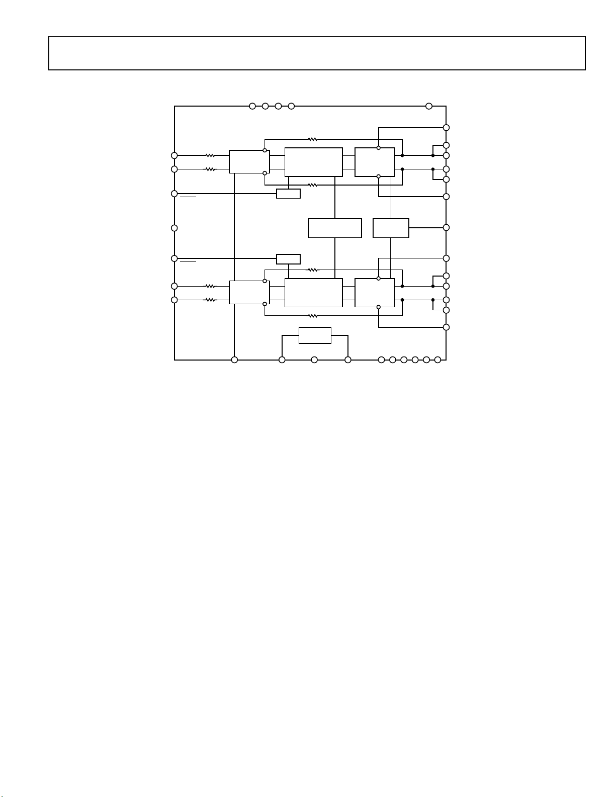
Data Sheet SSM3302
FUNCTIONAL BLOCK DIAGRAM
SSM3302
INR+
INR–
SDNR
MONO
SDNL
INL+
INL–
40kΩ
40kΩ
40kΩ
40kΩ
GAIN
PVDD
GAIN
CONTROL
GAIN
CONTROL
VREG
(AVDD) REGENAGND
MODULATOR
BIAS
BIAS
MODULATOR
(Σ-∆)
INTERNAL
OSCILLATOR
(Σ-∆)
VREG
FET
DRIVER
CONTROL
FET
DRIVER
EDGE
OUTR+
OUTR–
OUTL+
OUTL–
PGND
THERM
BOOTR+
BOOTR–
EDGE
BOOTL+
BOOTL–
10198-001
Figure 1.
Rev. 0 | Page 3 of 20
Page 4
SSM3302 Data Sheet
SPECIFICATIONS
PVDD = 12 V, TA = 25oC, RL = 8 Ω + 64 H, EDGE = AGND, gain = 9 dB, VREG = off, unless otherwise noted.
Table 1.
Parameter Symbol Test Conditions/Comments Min Typ Max Unit
DEVICE CHARACTERISTICS
Output Power/Channel P
O
R
R
R
R
R
R
R
R
R
R
R
Efficiency η PO = 7 W, 8 Ω, PVDD = 12 V, EDGE = low (normal operation) 91.5 %
Tot al H armoni c
THD + N P
Distortion + Noise
1.0 AVDD − 1 V
Input Common-Mode
V
CM
Voltage Range
Common-Mode
CMRR
Rejection Ratio
Channel Separation X
Average Switching
TAL K
300 kHz
f
SW
Frequency
Differential Output
V
OOS
Offset Voltage
POWER SUPPLY
Supply Voltage Range PVDD
Power Supply Rejection
PSRR
Ratio
PSRR
Supply Current (Stereo) I
SYPVDD
RL = 8 Ω, THD = 1%, f = 1 kHz, 20 kHz BW, PVDD = 15 V 121 W
= 8 Ω, THD = 1%, f = 1 kHz, 20 kHz BW, PVDD = 12 V 8 W
L
= 8 Ω, THD = 1%, f = 1 kHz, 20 kHz BW, PVDD = 7 V 2.7 W
L
= 8 Ω, THD = 10%, f = 1 kHz, 20 kHz BW, PVDD = 15 V 151 W
L
= 8 Ω, THD = 10%, f = 1 kHz, 20 kHz BW, PVDD = 12 V 10 W
L
= 8 Ω, THD = 10%, f = 1 kHz, 20 kHz BW, PVDD = 7 V 3.2 W
L
= 4 Ω, THD = 1%, f = 1 kHz, 20 kHz BW, PVDD = 15 V 201 W
L
= 4 Ω, THD = 1%, f = 1 kHz, 20 kHz BW, PVDD = 12 V 131 W
L
= 4 Ω, THD = 1%, f = 1 kHz, 20 kHz BW, PVDD = 7 V 4.8 W
L
= 4 Ω, THD = 10%, f = 1 kHz, 20 kHz BW, PVDD = 15 V 241 W
L
= 4 Ω, THD = 10%, f = 1 kHz, 20 kHz BW, PVDD = 12 V 161 W
L
= 4 Ω, THD = 10%, f = 1 kHz, 20 kHz BW, PVDD = 7 V 5.7 W
L
= 2 Ω, THD = 1%, f = 1 kHz, 20 kHz BW, PVDD = 12 V
R
L
29
2
W
(mono mode)
2
= 2 Ω, THD = 1%, f = 1 kHz, 20 kHz BW, PVDD = 7 V
R
L
9.4
W
(mono mode)
= 2 Ω, THD = 10%, f = 1 kHz, 20 kHz BW, PVDD = 12 V
R
L
36.6
2
W
(mono mode)
2
= 2 Ω, THD = 10%, f = 1 kHz, 20 kHz BW, PVDD = 7 V
R
L
12.7
W
(mono mode)
= 7 W, 8 Ω, PVDD = 12 V, EDGE = AVDD (ultralow
P
O
82 %
EMI mode)
= 5 W into 8 Ω, f = 1 kHz, PVDD = 12 V 0.01 %
O
VCM = 2.5 V ± 100 mV at 1 kHz, output referred 43 dB
PO = 0.5 W, f = 1 kHz 80 dB
Gain = 9 dB 3.0 mV
Guaranteed from PSRR test 7 18 V
PVDD = 7 V to 15 V, dc input floating 70 dB
DC
V
AC
= 100 mV at 1 kHz, inputs are ac grounded, CIN = 0.1 μF 80 dB
RIPPLE
VIN = 0 V, load = 8 Ω + 68 μH, PVDD = 15 V, V
(internal V
= 0 V, load = 8 Ω + 68 μH, PVDD = 15 V, V
V
IN
(internal V
= 0 V, load = 8 Ω + 68 μH, PVDD = 12 V, V
V
IN
(internal V
= 0 V, load = 8 Ω + 68 μH, PVDD = 7 V, V
V
IN
(internal V
active)
REG
disabled)
REG
disabled)
REG
disabled)
REG
REGEN
REGEN
REGEN
REGEN
= AVDD
= AGND
= AGND
= AGND
12.2 mA
6.2 mA
5 mA
3 mA
Rev. 0 | Page 4 of 20
Page 5
Data Sheet SSM3302
Parameter Symbol Test Conditions/Comments Min Typ Max Unit
I
Shutdown Current ISD
ANALOG SUPPLY
External Supply Voltage AVDD Permissible range for external AVDD, V
On-Board Regulator V
Regulator Current I
Regulator Power Supply
Rejection
GAIN CONTROL
Closed-Loop Voltage Gain AV See Table 5 for gain options 9 24 dB
Input Impedance Z
SHUTDOWN CONTROL
Input Voltage High V
Input Voltage Low V
Turn-On Time t
Turn-Off Time t
Output Impedance Z
AMPLIFIER PROTECTION
Overcurrent Threshold IOC 6 A
Overtemperature
Warning
Overtemperature
Shutdown
Recovery Temperature T
NOISE PERFORMANCE
Output Voltage Noise en
Signal-to-Noise Ratio SNR PO = 10 W, RL = 8 Ω 98 dB
1
Although the SSM3302 has good audio quality above 2 × 10 W into 4 Ω, continuous output power beyond 2 × 10 W into 4 Ω must be avoided due to device packaging
limitations.
2
Mono mode. Output power beyond 20 W needs special care for thermally considered printed circuit board (PCB) design.
SYAVDD
5 V
VREG
20 mA
VREG
PSRR
VREG
IN
IH
IL
WU
SD
OUT
120 °C
T
WARN
145 °C
T
SD
85 °C
REC
= 0 V, load = 8 Ω + 68 μH, PVDD = 15 V, V
V
IN
(internal V
= 0 V, load = 8 Ω + 68 μH, PVDD = 12 V, V
V
IN
(internal V
= 0 V, load = 8 Ω + 68 μH, PVDD = 7 V, V
V
IN
(internal V
= AGND
SD
disabled)
REG
disabled)
REG
disabled)
REG
REGEN
= AGND
REGEN
= AGND
REGEN
= AGND
REGEN
= AGND 4.5 5.5 V
70 dB
40 kΩ
1.35 V
0.35 V
SD rising edge from AGND to AVDD
SD falling edge from AVDD to AGND
= GND
SD
PVDD = 12 V, f = 20 Hz to 20 kHz, inputs are ac grounded,
5.85 mA
5.8 mA
5.6 mA
10 μA
40 ms
500 μs
56 kΩ
100 μV rms
gain = 9 dB, A-weighted
Rev. 0 | Page 5 of 20
Page 6
SSM3302 Data Sheet
ABSOLUTE MAXIMUM RATINGS
Absolute maximum ratings apply at 25°C, unless otherwise noted.
Table 2.
Parameter Rating
Power Supply Voltage (PVDD) −0.3 V to +25 V
Analog Supply Voltage (AVDD) −0.3 V to +6 V
Input Voltage −0.3 V to +6 V
ESD Susceptibility 4 kV
Storage Temperature Range −65°C to +150°C
Operating Temperature Range −40°C to +85°C
Junction Temperature Range −65°C to +165°C
Lead Temperature (Soldering, 60 sec) 300°C
Stresses above those listed under Absolute Maximum Ratings
may cause permanent damage to the device. This is a stress
rating only; functional operation of the device at these or any
other conditions above those indicated in the operational
section of this specification is not implied. Exposure to absolute
maximum rating conditions for extended periods may affect
device reliability.
THERMAL RESISTANCE
θJA (junction to air) is specified for the worst-case conditions,
that is, a device soldered in a circuit board for surface-mount
packages. θ
a 4-layer printed circuit board (PCB) with natural convection
cooling.
Table 3. Thermal Resistance
Package Type θJA θJC Unit
40-Lead, 6 mm × 6 mm LFCSP 31 2.5 °C/W
and θJC are determined according to JESD51-9 on
JA
ESD CAUTION
Rev. 0 | Page 6 of 20
Page 7

Data Sheet SSM3302
PIN CONFIGURATION AND FUNCTION DESCRIPTIONS
D
PVDD
PGND
PGND
PGN
37
38
39
40
D
PGND
PVDD
PVDD
PVDD
36
PGND
PGN
32
31
33
34
35
1BOOTL+
2OUTL+
3OUTL+
4OUTL–
5OUTL–
6BOOTL–
7AGND
8VREG/AVDD
9
SDNL
10EDGE
NOTES
1. USE MULTIPLE VIAS T O CONNECT THE EXPOSED PAD
TO THE G ROUND PLANE.
2. PINS LABELED NC CAN BE ALL OWED TO FLOAT,
BUT IT IS BETTER TO CONNECT THES E PINS TO
GROUND. AVOID ROUTING HIGH SPEED S IGNALS
THROUGH THESE PINS BECAUSE NOISE COUPLING
MAY RESULT.
SSM3302
TOP VIEW
(Not to Scale)
11
13
12
15
14
NC
EST
INL–
INL+
TEST
T
16
17
MONO
THERM
30 BOOTR+
29 OUTR+
28 OUTR+
27 OUTR–
26 OUTR–
25 BOOTR–
24 AGND
23 REGEN
22
SDNR
21 G AIN
18
20
19
C
N
INR–
INR+
10198-002
Figure 2. Pin Configuration (Top Side View)
Table 4. Pin Function Descriptions
Pin No. Mnemonic Description
1 BOOTL+ Bootstrap Input/Output for Left Channel, Noninverting Output.
2, 3 OUTL+ Noninverting Output for Left Channel.
4, 5 OUTL− Inverting Output for Left Channel.
6 BOOTL− Bootstrap Input/Output for Left Channel, Inverting Output.
7 AGND Analog Ground.
8 VREG/AVDD 5 V Regulator Output (if REGEN = high)/AVDD Input (if REGEN = low).
9
SDNL
Shutdown, Left Channel. Active low digital input.
10 EDGE Edge Control (Low Emission Mode). Active high digital input.
11 INL+ Noninverting Input for Left Channel.
12 INL− Inverting Input for Left Channel.
13, 18 NC This pin is not connected internally (see Figure 2).
14, 15 TEST Test Pins. Tie to AGND.
16 MONO Mono Output Mode Enable.
17 THERM Overtemperature Warning (Open Collector).
19 INR− Inverting Input for Right Channel.
20 INR+ Noninverting Input for Right Channel.
21 GAIN Gain Select from 9 dB to 24 dB.
22
SDNR
Shutdown, Right Channel. Active low digital input.
23 REGEN 5 V Regulator Enable, Active High.
24 AGND Analog Ground.
25 BOOTR− Bootstrap Input/Output for Right Channel, Inverting Output.
26, 27 OUTR− Inverting Output for Right Channel.
28, 29 OUTR+
Noninverting Output for Right Channel.
30 BOOTR+ Bootstrap Input/Output for Right Channel, Noninverting Output.
31, 32, 33, 38, 39, 40 PGND Power Stage Ground.
34, 35, 36, 37 PVDD Power Stage Power Supply.
Exposed Pad Thermal Exposed Pad. Use multiple vias to connect this pad to the ground plane.
Rev. 0 | Page 7 of 20
Page 8

SSM3302 Data Sheet
TYPICAL PERFORMANCE CHARACTERISTICS
Unless otherwise stated, all data at PVDD = 12 V, EDGE = low, MONO = low, REGEN = high, and GAIN = 9 dB.
100
RL = 8Ω + 33µH
GAIN = 9dB
EDGE = LOW
10
PVDD = 7V
PVDD = 12V
100
RL = 8Ω + 33µH
GAIN = 9dB
PVDD = 12V
10
1
0.1
THD + N (%)
0.01
0.001
0.0001 0.001 0. 01 0.1 1 10 100
PVDD = 18V
OUTPUT POWER (W )
Figure 3. THD + N vs. Output Power into 8 Ω;
PVDD = 7 V, PVDD = 12 V, PVDD = 18 V
100
RL = 4Ω + 15µH
GAIN = 9dB
EDGE = LOW
10
1
0.1
THD + N (%)
0.01
0.001
0.0001 0.001 0. 01 0.1 1 10 100
OUTPUT POWER (W )
PVDD = 7V
PVDD = 12V
PVDD = 18V
Figure 4. THD + N vs. Output Power into 4 Ω;
PVDD = 7 V, PVDD = 12 V, PVDD = 18 V
1
0.1
THD + N (%)
EDGE = LOW
0.01
0.001
1µ 1m0.1m0.01m 10m 100m 1 10 100
10198-003
EDGE = HIGH
OUTPUT POWER (W )
10198-006
Figure 6. THD + N vs. Output Power into 8 Ω;
EDGE = High, EDGE = Low
100
RL = 4Ω + 15µH
GAIN = 9dB
10
1
0.1
THD + N (%)
EDGE = LOW
0.01
0.001
1µ 1m0.1m0.01m 10m 100m 1 10 100
10198-004
EDGE = HIGH
OUTPUT POWER (W)
10198-007
Figure 7. THD + N vs. Output Power into 4 Ω;
EDGE = High, EDGE = Low
100
RL = 2Ω + 7.5µH
GAIN = 9dB
10
1
0.1
THD + N (%)
0.01
0.001
0.0001
1µ 1m0.1m0.01m 10m 100m 1 10 100
OUTPUT POWER (W)
PVDD = 7V
PVDD = 12V
PVDD = 18V
Figure 5. THD + N vs. Output Power into 2 Ω;
Mono Mode; Gain = 9 dB; PVDD = 7 V, PVDD = 12 V, 1 PVDD = 8 V
10198-005
Rev. 0 | Page 8 of 20
100
RL = 2Ω + 7.5µH
GAIN = 9dB
10
1
0.1
THD + N (%)
0.01
0.001
0.0001
1µ 1m0.1m0.01m 10m 100m 1 10 100
EDGE = HIGH
OUTPUT POWER (W)
EDGE = LOW
Figure 8. THD + N vs. Output Power into 2 Ω;
EDGE = High, EDGE = Low
10198-008
Page 9

Data Sheet SSM3302
100
10
PVDD = 7V
= 8Ω + 33µH
R
L
GAIN = 9dB
EDGE = LOW
PO = 2.5W
100
10
PVDD = 12V
= 8Ω + 33µH
R
L
GAIN = 9dB
EDGE = LOW
PO = 7.5W
1
0.1
THD + N (%)
PO = 0.25W
0.01
0.001
10 10k1k100 100k
PO = 0.5W
FREQUENCY (Hz)
Figure 9. THD + N vs. Frequency;
R
= 8 Ω; PVDD = 7 V; PO = 0.25 W, PO = 0.5 W, PO = 2.5 W
L
100
PVDD = 7V
= 4Ω + 15µH
R
L
GAIN = 9dB
10
EDGE = LOW
1
0.1
THD + N (%)
0.01
0.001
10 10k1k100 100k
PO = 5W
PO = 0.5W
PO = 2.5W
FREQUENCY (Hz)
Figure 10. THD + N vs. Frequency;
= 4 Ω; PVDD = 7 V; PO = 0.5 W, PO = 2.5 W, PO = 5 W
R
L
100
PVDD = 7V
= 2Ω + 7.5µH
R
L
GAIN = 9dB
10
EDGE = 0V
MONO = 5V
PO = 3.5W
1
0.1
THD + N (%)
0.01
0.001
10 10k1k100 100k
10198-009
FREQUENCY (Hz)
PO = 2.5W
= 5W
P
O
10198-012
Figure 12. THD + N vs. Frequency;
R
= 8 Ω; PVDD = 12 V; PO = 2.5 W, PO = 5 W, PO = 7.5 W
L
100
PVDD = 12V
= 4Ω + 15µH
R
L
GAIN = 9dB
10
EDGE = LOW
1
0.1
THD + N (%)
PO = 2.5W
0.01
0.001
10 10k1k100 100k
10198-010
PO = 5W
P
FREQUENCY (Hz)
= 10W
O
10198-013
Figure 13. THD + N vs. Frequency;
= 4 Ω; PVDD = 12 V; PO = 2.5 W, PO = 5 W, PO = 10 W
R
L
100
PVDD = 12V
= 4Ω + 7.5µH
R
L
GAIN = 9dB
10
EDGE = LOW
MONO = 5V
1
0.1
THD + N (%)
0.01
0.001
10 10k1k100 100k
PO = 0.5W
PO = 2.5W
FREQUENCY (Hz)
Figure 11. THD + N vs. Frequency;
= 2 Ω; Mono Mode; PVDD = 7 V; PO = 0.5 W, PO = 2.5 W, PO = 3.5 W
R
L
10198-011
Rev. 0 | Page 9 of 20
1
0.1
THD + N (%)
0.01
0.001
10 10k1k100 100k
PO = 0.5W
PO = 2.5W
PO = 5W
FREQUENCY (Hz)
Figure 14. THD + N vs. Frequency;
= 2 Ω; Mono Mode; PVDD = 12 V; PO = 0.5 W, PO = 2.5 W, PO = 5 W
R
L
10198-014
Page 10

SSM3302 Data Sheet
100
PVDD = 18V
= 8Ω + 33µH
R
L
GAIN = 9dB
10
EDGE = LOW
1
0.1
THD + N (%)
0.01
0.001
10 10k1k100 100k
PO = 2.5W
FREQUENCY (Hz)
PO = 5W
PO = 10W
Figure 15. THD + N vs. Frequency;
= 8 Ω; PVDD = 18 V; PO = 2.5 W, PO = 5 W, PO = 10 W
R
L
100
PVDD = 18V
= 4Ω + 15µH
R
L
GAIN = 9dB
10
EDGE = 0
1
0.1
THD + N (%)
PO = 10W
0.01
0.001
10 10k1k100 100k
FREQUENCY (Hz)
PO = 5W
PO = 2.5W
Figure 16. THD + N vs. Frequency;
= 4 Ω; PVDD = 18 V; PO = 2.5 W, PO = 5 W, PO = 10 W
R
L
100
PVDD = 18V
= 2Ω + 7.5µH
R
L
GAIN = 9dB
10
EDGE = 0
MONO = 5V
10198-015
10198-016
16
14
12
10
QUIESCENT CURRENT (mA)
8Ω + 33µH
8
6
4
2
0
718
8 9 10 11 12 13 14 15 16 17
SUPPLY VOLTAGE (V)
NO LOAD
4Ω + 15µH
10198-018
Figure 18. Quiescent Current vs. Supply Voltage,
R
= 8 Ω + 33 μH, No Load, , RL = 4 Ω + 15 μH
L
16
14
12
10
8
6
4
QUIESCENT CURRENT (mA)
2
0
8 9 10 11 12 13 14 15 16 17
718
SUPPLY VOLTAGE (V)
NO LOAD
2Ω + 7.5µH
4Ω + 15µH
10198-019
Figure 19. Quiescent Current vs. Supply Voltage,
Mono Mode, No Load, R
25
RL = 8Ω + 33µH
GAIN = 9dB
EDGE = 0
20
= 4 Ω + 15 μH, RL = 2 Ω + 7.5 μH
L
1
0.1
THD + N (%)
0.01
0.001
10 10k1k100 100k
PO = 0.5W
PO = 2.5W
FREQUENCY (Hz)
PO = 5W
Figure 17. THD + N vs. Frequency;
= 2 Ω; Mono Mode; PVDD = 18 V; PO = 0.5 W, PO = 2.5 W, PO = 5 W
R
L
10198-017
Rev. 0 | Page 10 of 20
15
THD = 10%
10
THD + N = 1%
5
MAXIMUM OUTPUT POWER (W)
0
7
911131517
SUPPLY VOLTAGE (V)
Figure 20. Maximum Output Power vs. Supply Voltage;
R
= 8 Ω; THD + N = 1%, THD + N = 10%
L
10198-020
Page 11

Data Sheet SSM3302
30
RL = 4Ω + 15µH
GAIN = 9dB
EDGE = 0
25
20
15
10
MAXIMUM OUTPUT POWER (W)
5
0
715
8 9 10 11 12 13 14
THD = 10%
SUPPLY VOLTAGE (V)
THD + N = 1%
10198-021
Figure 21. Maximum Output Power vs. Supply Voltage;
= 4 Ω; THD + N = 1%, THD + N = 10%
R
L
60
RL = 2Ω + 7.5µH
GAIN = 9dB
EDGE = 0
50
MONO
40
30
20
MAXIMUM OUTPUT POWER (W)
10
0
7
THD = 10%
THD = 1%
911131517
SUPPLY VOLTAGE (V)
10198-022
Figure 22. Maximum Output Power vs. Supply Voltage;
= 2 Ω; Mono Mode; THD + N = 1%, THD + N = 10%
R
L
800
700
600
500
400
300
SUPPLY CURRENT (mA)
200
100
0
05.0
0.5 1.0 1.5 2.0 2. 5 3.0 3.5 4.0 4.5
PVDD = 7V
OUTPUT POW ER (W)
PVDD = 12V
RL = 8Ω + 33µH
GAIN = 9dB
REGEN = 5V
PVDD = 18V
10198-023
Figure 23. Supply Current vs. Output Power into 8 Ω;
PVDD = 7 V, PVDD = 12 V, PVDD = 18 V
800
700
600
500
400
300
SUPPLY CURRENT (mA)
200
100
0
04.5
0.5 1.0 1.5 2.0 2.5 3.0 3. 5 4.0
OUTPUT POW ER (W)
PVDD = 7V
PVDD = 12V
PVDD = 18V
RL = 4Ω + 15µH
GAIN = 9dB
REGEN = 5V
10198-024
Figure 24. Supply Current vs. Output Power into 4 Ω;
PVDD = 7 V, PVDD = 12 V, PVDD = 18 V
3500
3000
2500
2000
1500
1000
SUPPLY CURRENT (mA)
500
PVDD = 7V
0
5 101520253035
040
PVDD = 12V
OUTPUT POW ER (W)
PVDD = 18V
RL = 2Ω + 7.5µH
GAIN = 9dB
REGEN = 5V
10198-025
Figure 25. Supply Current vs. Output Power into 2 Ω;
Mono Mode; PVDD = 7 V, PVDD = 12 V, PVDD = 18 V
100
PVDD =7V
90
80
70
60
50
40
EFFICI ENCY (%)
30
20
10
0
05 3025201510
PVDD = 12V
PVDD = 18V
OUTPUT PO WER (W)
RL = 8Ω + 33µH
GAIN = 9dB
EDGE = LOW
10198-026
Figure 26. Efficiency vs. Output Power into 8 Ω;
PVDD = 7 V, PVDD = 12 V, PVDD = 18 V
Rev. 0 | Page 11 of 20
Page 12

SSM3302 Data Sheet
100
PVDD = 7V
90
80
70
60
50
40
EFFICI ENCY (%)
30
20
10
0
05 3025201510
PVDD = 12V
PVDD = 18V
OUTPUT PO WER (W)
Figure 27. Efficiency vs. Output Power into 4 Ω;
PVDD = 7 V, PVDD = 12 V, PVDD = 18 V
100
PVDD = 7V
90
80
70
60
50
40
EFFICI ENCY (%)
30
20
10
0
05 40353020 251510
PVDD = 12V
PVDD = 18V
OUTPUT PO WER (W)
Figure 28. Efficiency vs. Output Power into 2 Ω;
Mono Mode; PVDD = 7 V, PVDD = 12 V, PVDD = 18 V
100
EDGE = LOW
90
80
70
60
50
40
EFFICIENCY (%)
30
20
10
0
05 3025201510
EDGE = HIGH
OUTPUT PO WER (W)
Figure 29. Efficiency vs. Output Power into 8 Ω;
PVDD = 12 V; EDGE = High, EDGE = Low
RL = 4Ω + 15µH
GAIN = 9dB
EDGE = LOW
RL = 2Ω + 7.5µH
GAIN = 9dB
EDGE = LOW
10198-027
10198-028
10198-029
100
90
80
70
60
50
40
EFFICIENCY (%)
30
20
10
0
05 3025201510
EDGE = LOW
EDGE = HIGH
OUTPUT PO WER (W)
Figure 30. Efficiency vs. Output Power into 4 Ω;
PVDD = 12 V; EDGE = High, EDGE = Low
100
90
80
70
60
50
40
EFFICI ENCY (%)
30
20
10
0
05 3525 30201510
EDGE = LOW
EDGE = HIGH
OUTPUT PO WER (W)
Figure 31. Efficiency vs. Output Power into 2 Ω;
Mono Mode; PVDD = 12 V; EDGE = High, EDGE = Low
0
–10
–20
–30
–40
CMRR (dB)
–50
–60
–70
–80
20 20,0002,000200
Figure 32. CMRR vs. Frequency, V
FREQUENCY (Hz)
= 100 mV rms, AC-Coupled
RIPPLE
10198-030
10198-031
10198-032
Rev. 0 | Page 12 of 20
Page 13

Data Sheet SSM3302
0
–10
–20
–30
–40
–50
PSRR (dB)
–60
–70
–80
–90
10 10k1k100 100k
Figure 33. PSRR vs. Frequency, V
0
–20
–40
FREQUENCY (Hz)
= 100 mV rms
RIPPLE
10198-033
Figure 35. Turn-On Response
(Showing
SDNL
Pin or
SDNR
Pin Rising Edge and Output)
VDD = 5V
V
= 5V
A
V
= 0V
B
10198-038
–60
–80
CROSSTALK (dB)
–100
10198-039
–120
10 10k1k100 100k
FREQUENCY (Hz)
Figure 34. Crosstalk vs. Frequency,
= 0.5 W, RL = 8 Ω
P
O
10198-037
Figure 36. Turn-Off Response
(Showing
SDNL
Pin or
SDNR
Pin Falling Edge and Output)
Rev. 0 | Page 13 of 20
Page 14

SSM3302 Data Sheet
TYPICAL APPLICATION CIRCUITS
PV
470µF 10µF
2× 1µF
DD
7V TO 18V
OVERTEMP ERATURE
WARNING
RIGHT I NPUT+
RIGHT INPUT–
SHUTDOWN – RIGHT
SHUTDOWN – LEFT
LEFT INPUT+
LEFT INPUT–
GAIN SELECT
GAIN = 9dB, 12dB, 15dB, 18dB, or 24dB
0.1µF
0.1µF
0.1µF
0.1µF
SSM3302
INR+
INR–
SDNR
MONO
SDNL
INL+
INL–
R
40kΩ
40kΩ
40kΩ
40kΩ
GAIN
PVDD
GAIN
GAIN
CONTROL
GAIN
CONTROL
VREG/
AVDD REGENAGND
5V
2.2µF
MODULATO R
BIAS
BIAS
MODULATO R
Figure 37. Stereo Mode Configuration
(Σ-∆)
INTERNAL
OSCILLATOR
(Σ-∆)
VREG
FET
DRIVER
CONTROL
FET
DRIVER
REGULATOR
ENABLE
EDGE
OUTR+
OUTR–
OUTL+
OUTL–
PGND
THERM
BOOTR+
BOOTR–
EDGE
BOOTL+
BOOTL–
0.22µF
0.22µF
EMISSION
CONTROL
0.22µF
0.22µF
10198-034
Rev. 0 | Page 14 of 20
Page 15

Data Sheet SSM3302
PV
470µF 10µF
2× 1µF
DD
7V TO 18V
OVERTEMPERATURE
WARNING
AVD D
SHUTDOWN
0.1µF
INPUT+
INPUT–
0.1µF
GAIN SELECT
GAIN = 9dB, 12d B, 15dB, 18dB, or 24dB
SSM3302
INR+
INR–
SDNR
MONO
SDNL
INL+
INL–
R
40kΩ
40kΩ
40kΩ
40kΩ
GAIN
GAIN
PVDD
GAIN
CONTROL
GAIN
CONTROL
VREG/
AVDD REG ENAGND
5V
2.2µF
MODULATOR
BIAS
BIAS
MODULATOR
(Σ-∆)
INTERNAL
OSCILLAT OR
(Σ-∆)
VREG
FET
DRIVER
CONTROL
FET
DRIVER
REGULATOR
ENABLE
Figure 38. Mono Mode Configuration
EDGE
OUTR+
OUTR–
OUTR+
OUTR–
PGND
THERM
BOOTR +
BOOTR –
EDGE
BOOTR +
BOOTR –
0.22µF
0.22µF
EMISSION
CONTROL
0.22µF
0.22µF
10198-035
Rev. 0 | Page 15 of 20
Page 16

SSM3302 Data Sheet
APPLICATIONS INFORMATION
OVERVIEW
The SSM3302 stereo Class-D audio amplifier features a filterless
modulation scheme that greatly reduces the external component
count, conserving board space and reducing system cost. The
SSM3302 does not require an output filter; it relies on the inherent
inductance of the speaker coil and the natural filtering of the
speaker and human ear to recover the audio component of the
square wave output.
Most Class-D amplifiers use some variation of pulse-width
modulation (PWM), but the SSM3302 uses Σ- modulation to
determine the switching pattern of the output devices, resulting in
several important benefits. Unlike pulse-width modulators, Σ-
modulators do not produce a sharp peak with many harmonics in
the AM broadcast band. In addition, Σ- modulation reduces the
amplitude of spectral components at high frequencies, reducing
EMI emission that might otherwise be radiated by speakers and
long cable traces. Due to the inherent spread spectrum nature of
Σ- modulation, the need for oscillator synchronization is eliminated for designs incorporating multiple SSM3302 amplifiers.
The SSM3302 also integrates overcurrent and overtemperature
protection, as well as an overtemperature warning indicator pin.
ANALOG SUPPLY
The SSM3302 includes an integrated low dropout (LDO) linear
regulator to generate a 5 V supply for the input stage. This regulator
can be enabled using the REGEN pin. This analog supply voltage is
available at the VREG/AVDD pin. Connect a 2.2 µF decoupling
capacitor from this pin to the AGND pin.
Alternatively, an external 5 V analog supply can be connected to
the AVDD pin. In this case, tie REGEN low to disable the
internal regulator.
The internal 5 V regulator can supply up to 20 mA of current to
the VREG pin if other analog circuits use the same supply. The
regulator includes short-circuit protection, but no current
limiter or other protection is provided.
GAIN SELECTION
The preset gain of SSM3302 can be selected between 9 dB and
24 dB with one external resistor and no change to the input impedance. Gain can be further adjusted to a user-defined setting by
inserting series external resistors at the inputs. A major benefit
of fixed input impedance is that there is no need to recalculate
the input corner frequency (f
input coupling components can be used for all gain settings.
Table 5. Gain Function Descriptions
Gain Setting (dB) GAIN Pin Configuration
24 Tie to AVDD
18 Tie to AVDD through 47 kΩ
15 Open
12 Tie to AGND through 47 kΩ
9 Tie to AGND
) when gain is adjusted. The same
c
Rev. 0 | Page 16 of 20
AMPLIFIER PROTECTION
The SSM3302 includes protection circuitry to prevent damage
in case of overcurrent and overtemperature conditions. Shorts
across the output terminals, or between either terminal and
PVDD or PGND, are also detected; in this case, the output
transistors do not switch until the fault is removed.
If the temperature exceeds the threshold temperature (approximately 145°C), the chip is disabled until the temperature drops
below the recovery threshold (85°C). This hysteresis prevents
rapid cycling of the output at high temperatures.
Additionally, a temperature warning signal is available on the
THERM pin. If the die temperature rises above 120°C, a logic
high is output on this pin.
POP-AND-CLICK SUPPRESSION
Voltage transients at the outputs of the audio amplifiers may occur
when shutdown is activated or deactivated. Voltage transients as
small as 10 mV can be heard as an audible pop in the speaker.
Clicks and pops are defined as undesirable audible transients
generated by the amplifier system that do not come from the
system input signal.
Such transients may be generated when the amplifier system
changes its operating mode. For example, system power-up and
power-down can be sources of audible transients.
The SSM3302 has a pop-and-click suppression architecture that
reduces these output transients, resulting in noiseless activation
and deactivation.
EMI NOISE
The SSM3302 uses a proprietary modulation and spread spectrum
technology to minimize EMI emissions from the device. The
SSM3302 can pass FCC Class-B emissions testing with unshielded
20 inch cable using ferrite bead-based filtering. For applica
tions that have difficulty passing FCC Class-B emission tests, the
SSM3302 includes a modulation select pin (ultralow EMI emission
mode) that significantly reduces the radiated emissions at the
Class-D outputs, particularly above 100 MHz. Note that reducing
the supply voltage greatly reduces radiated emissions.
MONO MODE
The SSM3302 can also be configured to stack its stereo outputs
into a monaural amplifier configuration by enabling the mono
output mode using the MONO pin. The user can drive a load as
small as 2 Ω up to 20 W continuous output power—a particularly
useful feature for driving the subwoofer in a 2.1 audio system.
To activate this operation, pull up the MONO pin to the level of
VREG/AVDD. In mono mode, OUTL+ and OUTR+ (Pin 2/Pin 3
and Pin 28/Pin 29) provide the noninverting output, and OUTL−
and OUTR− (Pin 4/Pin 5 and Pin 26/Pin 27) provide the inverting
output. While the device is in mono mode, audio input is taken
only from the left channel set of inputs: INL+ and INL− (Pin 11
and Pin 12).
Page 17

Data Sheet SSM3302
Because the mono mode uses output sense circuitry attached to
the left channel outputs, run PCB traces directly from the speaker
to the left channel outputs and then extend the PCB traces to
the right channel outputs.
OUTPUT MODULATION DESCRIPTION
The SSM3302 uses three-level, Σ- output modulation. Each
output can swing from PGND to PVDD and vice versa. Ideally,
when no input signal is present, the output differential voltage is
0 V because there is no need to generate a pulse. In a real-world
situation, however, there are always noise sources present.
Due to this constant presence of noise, a differential pulse is
occasionally generated in response to this stimulus. A small
amount of current flows into the inductive load when the
differential pulse is generated. However, most of the time, the
output differential voltage is 0 V. This feature ensures that the
current flowing through the inductive load is small.
When the user sends an input signal, an output pulse is generated
to follow the input voltage. The differential pulse density is
increased by raising the input signal level. Figure 39 depicts threelevel, Σ- output modulation with and without input stimulus.
OUTPUT = 0V
OUTR+/
OUTL+
OUTR–/
OUTL–
VOUT
OUTPUT > 0V
OUTR+/
OUTL+
OUTR–/
OUTL–
VOUT
OUTPUT < 0V
OUTR+/
OUTL+
OUTR–/
OUTL–
VOUT
Figure 39. Three-Level, Σ-Δ Output Modulation With and
Without Input Stimulus
+5V
0V
+5V
0V
+5V
0V
–5V
+5V
0V
+5V
0V
+5V
0V
+5V
0V
+5V
0V
0V
–5V
LAYOUT
As output power increases, care must be taken to lay out PCB traces
and wires properly among the amplifier, load, and power supply;
a poor layout increases voltage drops, consequently decreasing
efficiency. A good practice is to use short, wide PCB tracks to
decrease voltage drops and minimize inductance. For lowest DCR
10198-036
and minimum inductance, ensure that track widths are at least
200 mil for every inch of length and use 1 oz. or 2 oz. copper. Use
large traces for the power supply inputs and amplifier outputs.
Proper grounding guidelines help to improve audio performance,
minimize crosstalk between channels, and prevent switching
noise from coupling into the audio signal.
To maintain high output swing and high peak output power,
ensure that the PCB traces that connect the output pins to the
load and supply pins are as wide as possible to maintain the
minimum trace resistances. It is also recommended that a large
ground plane be used for minimum impedances. In addition,
good PCB layout isolates critical analog paths from sources of
high interference. High frequency circuits (analog and digital)
should be separated from low frequency circuits.
Properly designed multilayer PCBs can reduce EMI emission
and increase immunity to the RF field by a factor of 10 or more
compared with double-sided boards. A multilayer board allows
a complete layer to be used for the ground plane, whereas the
ground plane side of a double-sided board is often disrupted by
signal crossover.
If the system has separate ground planes for small signal and
high power connections, there should be no overlap between
these planes. Stitch the power plane to the SSM3302 exposed pad
using multiple vias. Proper layout improves heat conduction
into the board, allowing operation at larger output power levels
without overtemperature issues.
INPUT CAPACITOR SELECTION
Input capacitors are required if the input signal is not biased within
the recommended input dc common-mode voltage range, if
high-pass filtering is needed, or if a single-ended source is used.
If high-pass filtering is needed at the input, the input capacitor
and the input resistor of the SSM3302 form a high-pass filter
with a corner frequency determined by the following equation:
f
= 1/(2π × RIN × CIN)
C
The input capacitor can significantly affect the performance of
the circuit. Failure to use input capacitors degrades the output
offset of the amplifier.
BOOTSTRAP CAPACITORS
The output stage of the SSM3302 uses a high-side NMOS driver,
rather than PMOS driver. To generate the gate drive voltage for
the high-side NMOS driver, a bootstrap capacitor for each output
terminal acts as a floating power supply for the switching cycle.
Using 0.22 F ceramic capacitors with a voltage rating of 6.3 V
or greater is recommended.
Rev. 0 | Page 17 of 20
Page 18

SSM3302 Data Sheet
POWER SUPPLY DECOUPLING
To ensure high efficiency, low total harmonic distortion, and high
power supply rejection ratio, proper power supply decoupling
is necessary. Noise transients on the power supply lines are
short-duration voltage spikes. These spikes can contain frequency
components that extend into the hundreds of megahertz. Decouple
the power supply input with a good quality, low ESL, low ESR
bulk capacitor larger than 220 µF. This capacitor bypasses low
frequency noises to the ground plane.
For high frequency transient noises, place two separate 1 µF
capacitors as close as possible to the PVDD pins of the device.
Connect one of the 1 µF capacitors between the left-side PVDD
terminals and PGND terminals, and connect the other 1 µF
capacitor between the right-side PVDD terminals and PGND
terminals. Placing the decoupling capacitor as close as possible
to the SSM3302 helps to achieve the best performance.
Rev. 0 | Page 18 of 20
Page 19

Data Sheet SSM3302
OUTLINE DIMENSIONS
PIN 1
INDICATOR
6.10
6.00 SQ
5.90
0.50
BSC
0.30
0.23
0.18
31
1
P
N
30
EXPOSED
PAD
40
1
I
N
I
D
4.45
4.30 SQ
4.25
R
O
C
I
A
T
0.80
0.75
0.70
SEATING
PLANE
21
0.08
20
BOTTOM VIEWTOP VIEW
0.45
0.40
0.35
0.05 MAX
0.02 NOM
COPLANARITY
0.20 REF
COMPLIANT TO JEDEC ST ANDARDS MO-220-WJJD.
10
11
0.25 MIN
FOR PROPER CO NNECTION OF
THE EXPOSED PAD, REFER TO
THE PIN CONF IGURATIO N AND
FUNCTION DESCRI PTIONS
SECTION O F THIS DATA S HEET.
05-06-2011-A
Figure 40. 40-Lead Lead Free Chip Scale Package [LFCSP_WQ]
6 mm × 6 mm Body, Very Very Thin Quad
(CP-40-10)
Dimensions shown in millimeters
ORDERING GUIDE
Model1 Temperature Range Package Description Package Option
SSM3302ACPZ −40°C to +85°C 40-Lead Lead Free Chip Scale Package [LFCSP_WQ] CP-40-10
SSM3302ACPZ-RL −40°C to +85°C 40-Lead Lead Free Chip Scale Package [LFCSP_WQ] CP-40-10
SSM3302ACPZ-R7 −40°C to +85°C 40-Lead Lead Free Chip Scale Package [LFCSP_WQ]
EVAL-SSM3302Z Evaluation Board
1
Z = RoHS Compliant Part.
CP-40-10
Rev. 0 | Page 19 of 20
Page 20

SSM3302 Data Sheet
NOTES
©2012 Analog Devices, Inc. All rights reserved. Trademarks and
registered trademarks are the property of their respective owners.
D10198-0-2/12(0)
Rev. 0 | Page 20 of 20
 Loading...