

Page 1
Low Power Audio Codec
FEATURES
Stereo, 24-bit analog-to-digital and digital-to-analog converters
DAC SNR: 100 dB (A-weighted), THD: −80 dB at 48 kHz, 3.3 V
ADC SNR: 90 dB (A-weighted), THD: −80 dB at 48 kHz, 3.3 V
Stereo line inputs
Low power
7 mW stereo playback (1.8 V/1.5 V supplies)
14 mW record and playback (1.8 V/1.5 V supplies)
Low supply voltages
Analog: 1.8 V to 3.6 V
Digital: 1.5 V to 3.6 V
256/384 oversampling rate in normal mode;
250/272 oversampling rate in USB mode
Audio sampling rates: 8 kHz, 11.025 kHz, 12 kHz, 16 kHz,
22.05 kHz, 24 kHz, 32 kHz, 44.1 kHz, 48 kHz, 88.2 kHz,
and 96 kHz
20-lead, 4 mm × 4 mm LFCSP (QFN) package
APPLICATIONS
Mobile phones
MP3 players
Portable gaming
Portable electronics
Educational toys
SSM2604
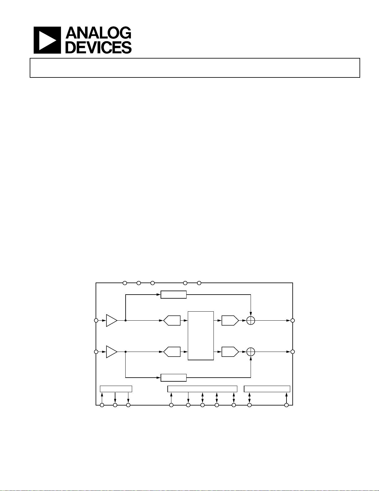
GENERAL DESCRIPTION
The SSM2604 is a low power, high quality stereo audio codec
for portable digital audio applications with one set of stereo
programmable gain amplifier (PGA) line inputs. It features two
24-bit analog-to-digital converter (ADC) channels and two
24-bit digital-to-analog (DAC) converter channels.
The SSM2604 can operate as a master or a slave. It supports
various master clock frequencies, including 12 MHz or 24 MHz
for USB devices; standard 256 f
12.288 MHz and 24.576 MHz; and many common audio sampling rates, such as 96 kHz, 88.2 kHz, 48 kHz, 44.1 kHz, 32 kHz,
24 kHz, 22.05 kHz, 16 kHz, 12 kHz, 11.025 kHz, and 8 kHz.
The SSM2604 can operate at power supplies as low as 1.8 V for
the analog circuitry and as low as 1.5 V for the digital circuitry.
The maximum voltage supply is 3.6 V for all supplies.
The SSM2604 is specified over the industrial temperature range
of −40°C to +85°C. It is available in a 20-lead, 4 mm × 4 mm
lead frame chip scale package (LFCSP).
or 384 fS based rates, such as
S
FUNCTIONAL BLOCK DIAGRAM
AVDDVMID AGND DVDD DGND
BYPASS
–34.5dB TO +33dB,
1.5dB STEP
RLINEIN
LLINEIN
–34.5dB TO +33dB,
1.5dB STEP
CLK
MCLK/
XTO CLKOUT
XTI
Rev. 0
Information furnished by Analog Devices is believed to be accurate and reliable. However, no
responsibility is assumed by Analog Devices for its use, nor for any infringements of patents or other
rights of third parties that may result from its use. Specifications subject to change without notice. No
license is granted by implication or otherwise under any patent or patent rights of Analog Devices.
Trademarks and registered trademarks are the property of their respective owners.
ADC
ADC
BYPASS
DIGITAL AUDIO INTERFACE
PBDAT RECDAT BCLK PBLRC RECLRC
SSM2604
DAC
DIGITAL
PROCESSOR
DAC
CONTROL I NTERFACE
SDIN SCLK
Figure 1.
One Technology Way, P.O. Box 9106, Norwood, MA 02062-9106, U.S.A.
Tel: 781.329.4700 www.analog.com
Fax: 781.461.3113 ©2008 Analog Devices, Inc. All rights reserved.
ROUT
LOUT
06978-001
Page 2

SSM2604
TABLE OF CONTENTS
Features .............................................................................................. 1
Applications ....................................................................................... 1
General Description ......................................................................... 1
Functional Block Diagram .............................................................. 1
Revision History ............................................................................... 2
Specifications ..................................................................................... 3
Digital Filter Characteristics ....................................................... 4
Timing Characteristics ................................................................ 5
Absolute Maximum Ratings ............................................................ 7
Thermal Resistance ...................................................................... 7
ESD Caution .................................................................................. 7
Pin Configuration and Function Descriptions ............................. 8
Typical Performance Characteristics ............................................. 9
Converter Filter Response ........................................................... 9
Digital De-Emphasis .................................................................. 10
Theory of Operation ...................................................................... 11
Digital Core ................................................................................. 11
ADC and DAC ............................................................................ 11
ADC High-Pass and DAC De-Emphasis Filters .................... 11
Analog Interface ......................................................................... 12
Digital Audio Interface .............................................................. 12
Software Control Interface ........................................................ 15
Typical Application Circuits ......................................................... 16
Register Map ................................................................................... 17
Register Map Details ...................................................................... 18
Left-Channel ADC Input Volume, Address 0x00 .................. 18
Right-Channel ADC Input Volume, Address 0x01 ............... 19
Analog Audio Path, Address 0x04 ........................................... 20
Digital Audio Path, Address 0x05 ............................................ 20
Power Management, Address 0x06 .......................................... 21
Digital Audio I/F, Address 0x07 ............................................... 22
Sampling Rate, Address 0x08 .................................................... 22
Active, Address 0x09 .................................................................. 25
Software Reset, Address 0x0F ................................................... 25
Outline Dimensions ....................................................................... 26
Ordering Guide .......................................................................... 26
REVISION HISTORY
7/08—Revision 0: Initial Version
Rev. 0 | Page 2 of 28
Page 3
SSM2604
SPECIFICATIONS
TA = 25°C, AVDD = DVDD = 3.3 V, 1 kHz signal, fS = 48 kHz, PGA gain = 0 dB, 24-bit audio data, unless otherwise noted.
Table 1.
Parameter Min Typ Max Unit Conditions
RECOMMENDED OPERATING CONDITIONS
Analog Voltage Supply (AVDD) 1.8 3.3 3.6 V
Digital Power Supply 1.5 3.3 3.6 V
Ground (AGND, DGND) 0 V
POWER CONSUMPTION
Power-Up
Stereo Record (1.5 V and 1.8 V) 7 mW
Stereo Record (3.3 V) 22 mW
Stereo Playback (1.5 V and 1.8 V) 7 mW
Stereo Playback (3.3 V) 22 mW
Power-Down 56 W
LINE INPUT
Input Signal Level (0 dB) 1 × AVDD/3.3 V rms
Input Impedance 200 kΩ PGA gain = 0 dB
10 kΩ PGA gain = +33 dB
480 kΩ PGA gain = −34.5 dB
Input Capacitance 10 pF
Signal-to-Noise Ratio (A-Weighted) 70 90 dB PGA gain = 0 dB, AVDD = 3.3 V
84 dB PGA gain = 0 dB, AVDD = 1.8 V
Total Harmonic Distortion (THD) −80 dB −1 dBFS input, AVDD = 3.3 V
−75 dB −1 dBFS input, AVDD = 1.8 V
Channel Separation 80 dB
Programmable Gain −34.5 0 +33.5 dB
Gain Step 1.5 dB
Mute Attenuation −80 dB
LINE OUTPUT
DAC −1 dBFS input DAC + line output
Full-Scale Output 1 × AVDD/3.3 V rms
Signal-to-Noise Ratio (A-Weighted) 85 100 dB AVDD = 3.3 V
94 dB AVDD = 1.8 V
THD + N −80 −75 dB AVDD = 3.3 V
−75 dB AVDD = 1.8 V
Power Supply Rejection Ratio 50 dB
Channel Separation 80 dB
LINE INPUT TO LINE OUTPUT
Full-Scale Output Voltage 1 × AVDD/3.3 V rms
Signal-to-Noise Ratio (A-Weighted) 92 dB AVDD = 3.3 V
86 dB AVDD = 1.8 V
Total Harmonic Distortion −80 dB AVDD = 3.3 V
−80 dB AVDD = 1.8 V
Power Supply Rejection 50 dB
Rev. 0 | Page 3 of 28
Page 4
SSM2604
DIGITAL FILTER CHARACTERISTICS
Table 2.
Parameter Min Typ Max Unit Conditions
ADC FILTER
Pass Band 0 0.445 fS Hz ±0.04 dB
0.5 fS Hz −6 dB
Pass-Band Ripple ±0.04 dB
Stop Band 0.555 fS Hz
Stop-Band Attenuation −61 dB f > 0.567 fS
High-Pass Filter Corner Frequency 3.7 Hz −3 dB
10.4 Hz −0.5 dB
21.6 Hz −0.1 dB
DAC FILTER
Pass Band 0 0.445 fS Hz ±0.04 dB
0.5 fS Hz −6 dB
Pass-Band Ripple ±0.04 dB
Stop Band 0.555 fS Hz
Stop-Band Attenuation −61 dB f > 0.565 fS
CORE CLOCK TOLERANCE
Frequency Range 8.0 13.8 MHz
Jitter Tolerance 50 ps
Rev. 0 | Page 4 of 28
Page 5
SSM2604
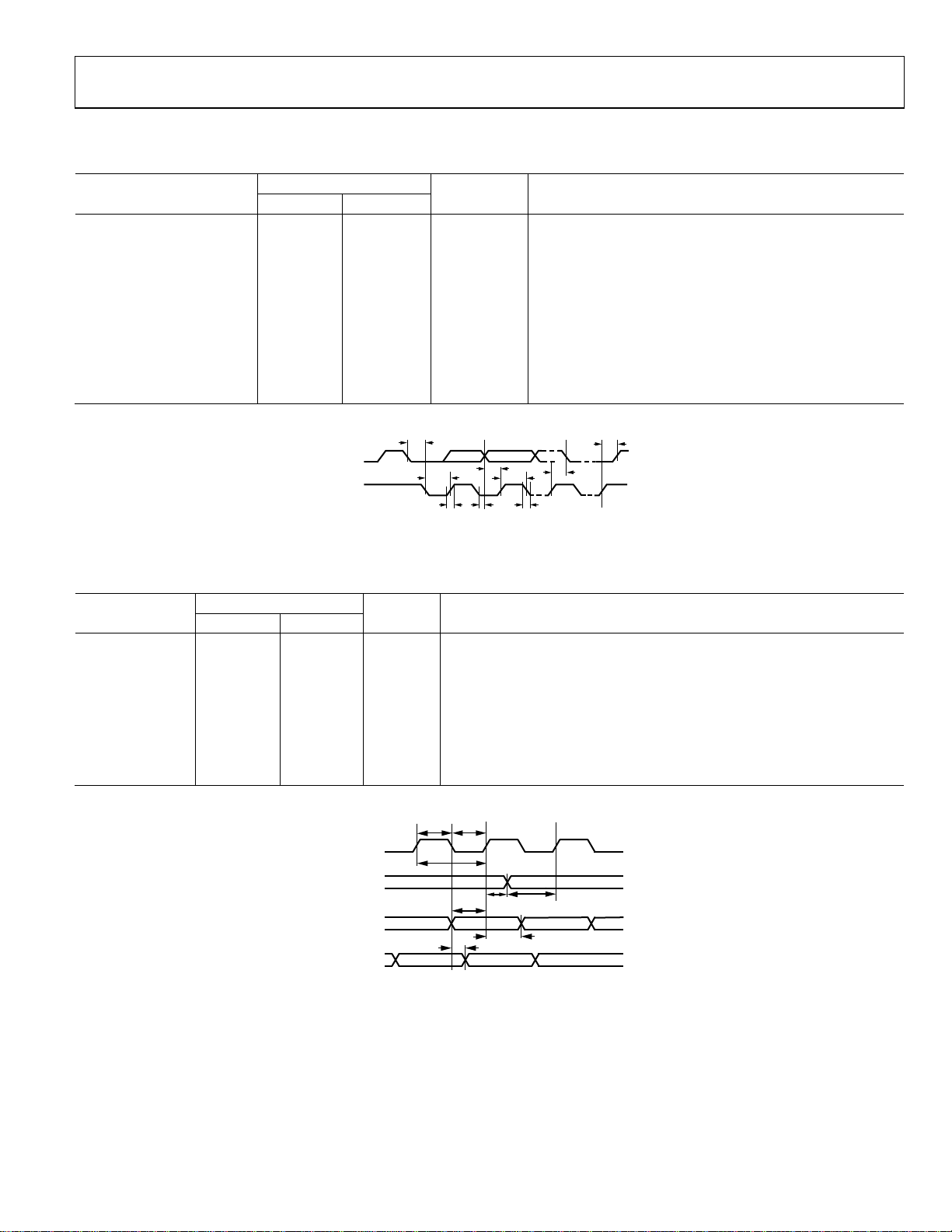
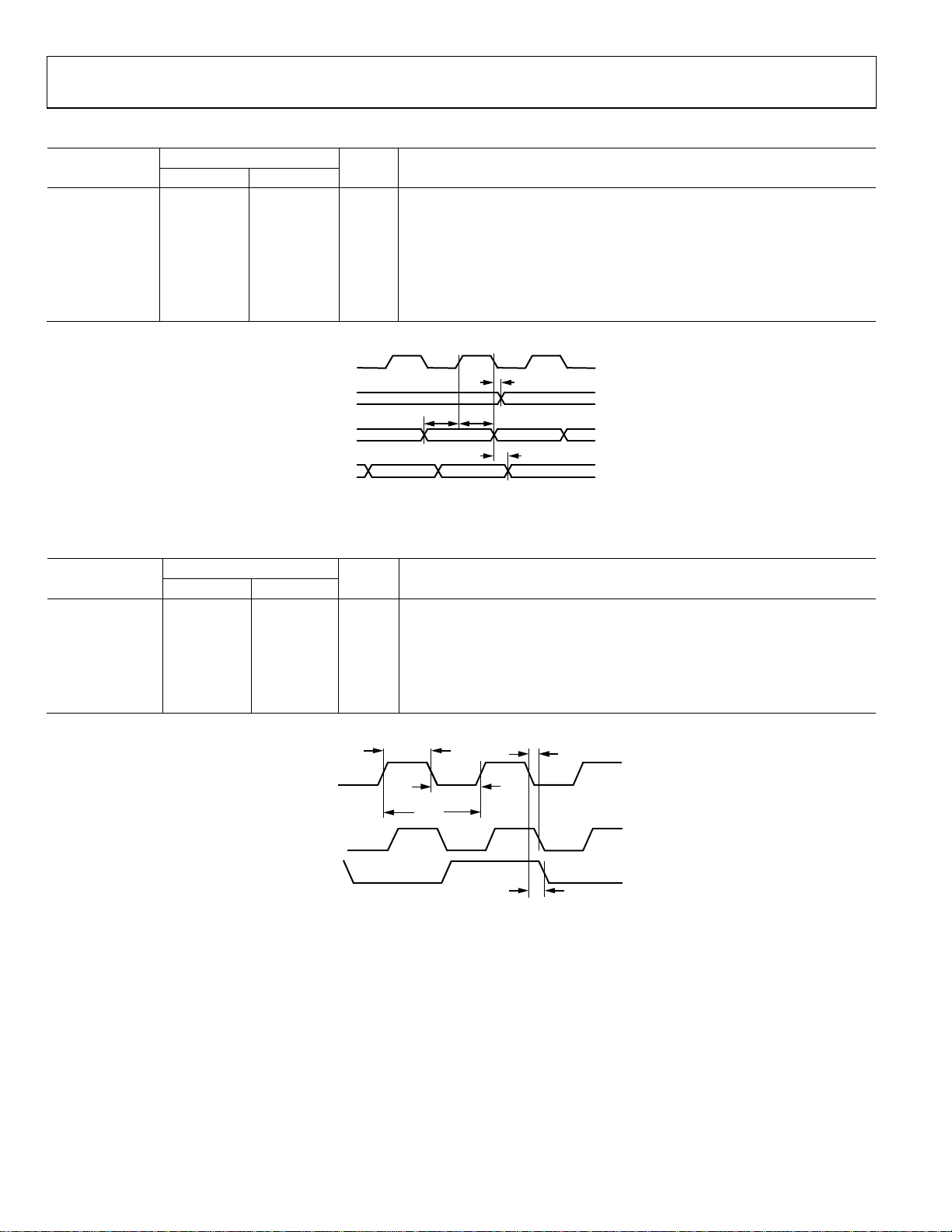
TIMING CHARACTERISTICS
Table 3. I2C Timing
Limit
Parameter t
t
600 ns Start condition setup time
SCS
t
600 ns Start condition hold time
SCH
tPH 600 ns SCLK pulse width high
tPL 1.3 µs SCLK pulse width low
f
0 526 kHz SCLK frequency
SCLK
tDS 100 ns Data setup time
tDH 900 ns Data hold time
tRT 300 ns SDIN and SCLK rise time
tFT 300 ns SDIN and SCLK fall time
t
600 ns Stop condition setup time
HCS
t
MIN
Unit Description
MAX
SDIN
SCLK
t
t
PL
t
RT
SCH
t
DS
Figure 2. I
t
PH
t
DH
2
C Timing
t
HCS
t
SCS
t
FT
06978-036
Table 4. Digital Audio Interface Slave Mode Timing
Parameter t
Limit
t
MIN
MAX
Unit Description
tDS 10 ns PBDAT setup time from BCLK rising edge
tDH 10 ns PBDAT hold time from BCLK rising edge
t
10 ns RECLRC/PBLRC setup time to BCLK rising edge
LRSU
t
10 ns RECLRC/PBLRC hold time to BCLK rising edge
LRH
tDD 30 ns RECDAT propagation delay from BCLK falling edge (external load of 70 pF)
t
25 ns BCLK pulse width high
BCH
t
25 ns BCLK pulse width low
BCL
t
50 ns BCLK cycle time
BCY
t
t
BCL
BCH
BCLK
PBLRC/
RECLRC
PBDAT
RECDAT
t
BCY
t
DS
t
t
LRSU
LRH
t
t
DD
DH
06978-025
Figure 3. Digital Audio Interface Slave Mode Timing
Rev. 0 | Page 5 of 28
Page 6
SSM2604
Table 5. Digital Audio Interface Master Mode Timing
Parameter t
t
30 ns PBDAT setup time to BCLK rising edge
DST
t
10 ns PBDAT hold time to BCLK rising edge
DHT
MIN
Limit
t
Unit Description
MAX
tDL 10 ns RECLRC/PBLRC propagation delay from BCLK falling edge
t
10 ns RECDAT propagation delay from BCLK falling edge
DDA
t
10 ns BCLK rising time (10 pF load)
BCLKR
t
10 ns BCLK falling time (10 pF load)
BCLKF
t
45:55:00 55:45:00 BCLK duty cycle (normal and USB mode)
BCLKDS
BCLK
t
PBLRC/
RECLRC
PBDAT
RECDAT
t
DSTtDHT
Figure 4. Digital Audio Interface Master Mode Timing
DL
t
DDA
6978-026
Table 6. System Clock Timing
Limit
Parameter t
t
72 ns MCLK/XTI system clock cycle time
XTIY
t
40:60 60:40:00 MCLK/XTI duty cycle
MCLKDS
t
32 ns MCLK/XTI system clock pulse width high
XTIH
t
32 ns MCLK/XTI system clock pulse width low
XTIL
t
20 ns CLKOUT propagation delay from MCLK/XTI falling edge
COP
t
20 ns CLKODIV2 propagation delay from MCLK/XTI falling edge
COPDIV2
t
MIN
Unit Description
MAX
MCLK/XTI
CLKOUT
CLKODI V2
t
XTIH
t
XTIL
t
XTIY
t
COPDIV2
Figure 5. System (MCLK) Clock Timing
t
COP
06978-035
Rev. 0 | Page 6 of 28
Page 7
SSM2604
ABSOLUTE MAXIMUM RATINGS
At 25°C, unless otherwise noted.
Table 7.
Parameter Rating
Supply Voltage 3.6 V
Input Voltage VDD
Common-Mode Input Voltage VDD
Storage Temperature Range −65°C to +150°C
Operating Temperature Range −40°C to +85°C
Junction Temperature Range −65°C to +165°C
Lead Temperature (Soldering, 60 sec) 300°C
Stresses above those listed under Absolute Maximum Ratings
may cause permanent damage to the device. This is a stress
rating only; functional operation of the device at these or any
other conditions above those indicated in the operational
section of this specification is not implied. Exposure to absolute
maximum rating conditions for extended periods may affect
device reliability.
THERMAL RESISTANCE
θJA is specified for the worst-case conditions, that is, a device
soldered in a circuit board for surface-mount packages.
Table 8. Thermal Resistance
Package Type θJA θJC Unit
20-Lead, 4 mm × 4 mm LFCSP 28 32 °C/W
ESD CAUTION
Rev. 0 | Page 7 of 28
Page 8
SSM2604
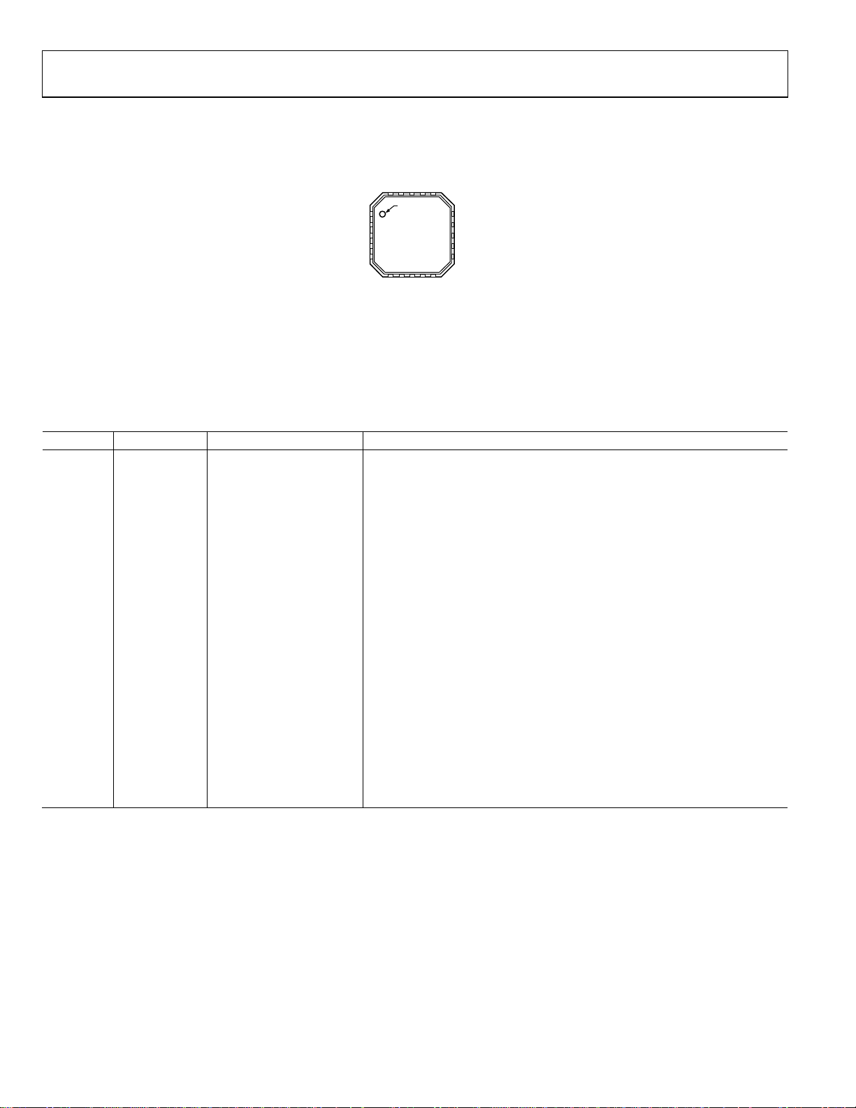
PIN CONFIGURATION AND FUNCTION DESCRIPTIONS
SDIN
SCLK
NC
LLINEIN
RLINEIN
17
16
18
19
20
PIN 1
INDICATOR
1MCLK/XTI
2XTO
SSM2604
3DGND
TOP VIEW
4DVDD
(Not to Scale)
5CLKOUT
6
7
CLK
B
NOTES
1. NC = NO CONNE CT.
2. FOR PROPER CONNECTION OF THE EXPOSED PAD,
CONNECT TO PCB GROUND LAYER
PBDAT
Figure 6. Pin Configuration
Table 9. Pin Function Descriptions
Pin No. Mnemonic Type Description
1 MCLK/XTI Digital Input Master Clock Input/Crystal Input.
2 XTO Digital Output Crystal Output.
3 DGND Digital Ground Digital Ground.
4 DVDD Digital Supply Digital Core and I/O Buffer Supply.
5 CLKOUT Digital Output Buffered Clock Output.
6 BCLK Digital Input/Output Digital Audio Bit Clock.
7 PBDAT Digital Input DAC Digital Audio Data Input, Playback Function.
8 PBLRC Digital Input/Output DAC Sampling Rate Clock, Playback Function (from Left and Right Channels).
9 RECDAT Digital Output ADC Digital Audio Data Output, Record Function.
10 RECLRC Digital Input/Output ADC Sampling Rate Clock, Record Function (from Left and Right Channels).
11 LOUT Analog Output Line Output for Left Channel.
12 ROUT Analog Output Line Output for Right Channel.
13 AVDD Analog Supply Analog Supply.
14 AGND Analog Ground Analog Ground.
15 VMID Analog Output Midrail Voltage Decoupling Input.
16 RLINEIN Analog Input Line Input for Right Channel.
17 LLINEIN Analog Input Line Input for Left Channel.
18 SDIN Digital Input/Output 2-Wire Control Interface Data Input/Output.
19 SCLK Digital Input 2-Wire Control Interface Clock Input.
20 NC NC No Connection
GND Pad Thermal Pad/Exposed Pad Center Thermal Pad. Connect to PCB ground layer.
15 VMID
14 AGND
13 AVDD
12 ROUT
11 LOUT
9
8
10
RC
PBL
RECLRC
RECDAT
06978-002
Rev. 0 | Page 8 of 28
Page 9
SSM2604
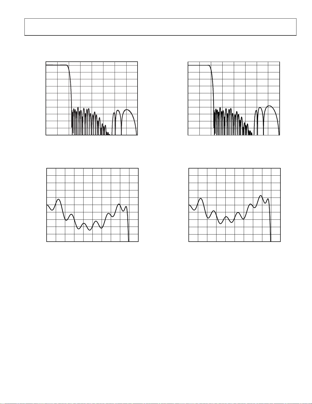
TYPICAL PERFORMANCE CHARACTERISTICS
CONVERTER FILTER RESPONSE
0
–10
–20
–30
–40
–50
–60
MAGNITUDE (dB)
–70
–80
–90
–100
00.25
0.75 1.00 1.250.50 1.50 2.00
FREQUENCY (
f
)
S
Figure 7. ADC Digital Filter Frequency Response
0.05
0.04
0.03
0.02
0.01
0
−0.01
MAGNITUDE (dB)
−0.02
−0.03
−0.04
−0.05
0 0.050.100.150.200.250.300.350.400.450.50
FREQUENCY (
f
)
S
Figure 8. ADC Digital Filter Ripple
1.75
0
–10
–20
–30
–40
–50
–60
MAGNITUDE (dB)
–70
–80
–90
–100
00.25
06978-003
0.75 1.00 1.250.50 1.50 2.001.75
FREQUENCY (
f
)
S
6978-005
Figure 9. DAC Digital Filter Frequency Response
0.05
0.04
0.03
0.02
0.01
0
−0.01
MAGNITUDE (d B)
−0.02
−0.03
−0.04
−0.05
0 0.050.100.150.200.250.300.350.400.450.50
6978-004
FREQUENCY (
f
)
S
6978-006
Figure 10. DAC Digital Filter Ripple
Rev. 0 | Page 9 of 28
Page 10

SSM2604
DIGITAL DE-EMPHASIS
0
−1
−2
−3
−4
−5
−6
MAGNITUDE (d B)
−7
−8
−9
−10
0 4 8 12 16
FREQUENCY (kHz)
06978-007
Figure 11. De-Emphasis Frequency Response, Audio Sampling Rate = 32 kHz
0.4
0.3
0.2
0.1
0
−0.1
MAGNITUDE (dB)
−0.2
−0.3
−0.4
04 12 20816
FREQUENCY (kHz)
Figure 14. De-Emphasis Error, Audio Sampling Rate = 44.1 kHz
06978-010
0.4
0.3
0.2
0.1
0
−0.1
MAGNITUDE (d B)
−0.2
−0.3
−0.4
04 1281
FREQUENCY (kHz)
6
Figure 12. De-Emphasis Error, Audio Sampling Rate = 32 kHz
0
−1
−2
−3
−4
−5
−6
MAGNITUDE (dB)
−7
−8
−9
−10
0 4 12 20816
FREQUENCY (kHz)
Figure 13. De-Emphasis Frequency Response, Audio Sampling Rate = 44.1 kHz
0
−1
−2
−3
−4
−5
−6
MAGNITUDE (d B)
−7
−8
−9
−10
0 4 12 20816
6978-008
FREQUENCY (kHz)
24
06978-011
Figure 15. De-Emphasis Frequency Response, Audio Sampling Rate = 48 kHz
0.4
0.3
0.2
0.1
0
−0.1
MAGNITUDE (d B)
−0.2
−0.3
−0.4
0 4 12 2081624
06978-009
FREQUENCY (kHz)
06978-012
Figure 16. De-Emphasis Error, Audio Sampling Rate = 48 kHz
Rev. 0 | Page 10 of 28
Page 11

SSM2604
THEORY OF OPERATION
DIGITAL CORE
Inside the SSM2604 digital core is a central clock source, called
the master clock (MCLK), that produces a reference clock for
all internal audio data processing and synchronization. When
using an external clock source to drive the MCLK pin, great
care should be taken to select a clock source with less than 50 ps
of jitter. Without careful generation of the MCLK signal, the
digital audio quality likely suffers.
To enable the SSM2604 to generate the central reference clock
in a system, connect a crystal oscillator between the MCLK/XTI
input pin and the XTO output pin.
To allow an external device to generate the central reference
clock, apply the external clock signal directly through the MCLK/
XTI input pin. In this configuration, the oscillator circuit of the
SSM2604 can be powered down by using the OSC bit (Register
R6, Bit D5) to reduce power consumption.
To accommodate applications with very high frequency master
clocks, the internal core reference clock of the SSM2604 can be
set to either MCLK or MCLK divided by 2. This is enabled by
adjusting the setting of the CLKDIV2 bit (Register R8, Bit D6).
Complementary to this feature, the CLKOUT pin can also drive
external clock sources with either the core clock signal or the
core clock divided by 2 by enabling the CLKODIV2 bit
(Register R8, Bit D7).
ADC AND DAC
The SSM2604 contains a pair of oversampling Σ-Δ ADCs.
The maximum ADC full-scale input level is 1.0 V rms when
AVDD = 3.3 V. If the input signal to the ADC exceeds this
level, data overloading occurs and causes audible distortion.
The ADC accepts analog audio input from the stereo line
inputs. The digital data from the ADC output, once converted,
is processed using the ADC filters.
Complementary to the ADC channels, the SSM2604 contains a
pair of oversampling Σ-Δ DACs that convert the digital audio
data from the internal DAC filters into an analog audio signal.
The DAC output can also be muted by setting the DACMU bit
(Register R5, Bit D3) in the control register.
ADC HIGH-PASS AND DAC DE-EMPHASIS FILTERS
The ADC and DAC employ separate digital filters that perform
24-bit signal processing. The digital filters are used for both
record and playback modes and are optimized for each individual sampling rate used.
For recording mode operations, the unprocessed data from the
ADC enters the ADC filters and is converted to the appropriate
sampling frequency, and then is output to the digital audio
interface.
For playback mode operations, the DAC filters convert the digital
audio interface data to oversampled data, using a sampling rate
selected by the user. The oversampled data is processed by the
DAC and then is sent to the analog output mixer by enabling
the DACSEL (Register R4, Bit D4).
Users have the option of setting up the device so that any dc
offset in the input source signal is automatically detected and
removed. To accomplish this, enable the digital high-pass filter
(see Tabl e 2 for characteristics) contained in the ADC digital
filters by using the ADCHPF bit (Register R5, Bit D0).
In addition, users can implement digital de-emphasis by using
the DEEMPH bits (Register R5, Bit D1 and Bit D2).
Rev. 0 | Page 11 of 28
Page 12

SSM2604
ANALOG INTERFACE
Signal Chain
The SSM2604 includes stereo single-ended line inputs to the
on-board ADC. In addition, the line inputs can be routed and
mixed directly to the output terminals via the BYPASS bit
(Register R4, Bit D3). The SSM2604 also includes line outputs
from the on-board DAC.
Stereo Line Inputs
The SSM2604 contains a set of single-ended stereo line inputs
(RLINEIN and LLINEIN) that are internally biased to VMID
by way of a voltage divider between AVDD and AGND. The
line input signal can be connected to the internal ADC and, if
desired, routed directly to the outputs via the bypass path by
using the BYPASS bit (Register R4, Bit D3).
LINEIN
AVDD
–
VMID
AGND
Figure 17. Line Input to ADC
+
The line input volume can be adjusted from −34.5 dB to +33 dB
in steps of +1.5 dB by setting the LINVOL (Register R0, Bit D0
to Bit D5) and RINVOL (Register R1, Bit D0 to Bit D5) bits.
Volume control, by default, is independently adjustable on
both right and left line inputs. However, the LRINBOTH or
RLINBOTH bit, if selected, simultaneously loads both sets of
volume control with the same value. The user can also set the
LINMUTE (Register R0, Bit D7) and RINMUTE (Register R1,
Bit D7) bits to mute the line input signal to the ADC.
Note that when sourcing audio data from line inputs, the maximum full-scale input of the ADC is 1.0 V rms when AVDD = 3.3 V.
Do not source any input voltage larger than full scale to avoid
overloading the ADC, which causes distortion of sound and
deterioration of audio quality. For best sound quality in line
inputs, gain should be carefully configured so that the ADC
receives a signal equal to its full scale. This maximizes the
signal-to-noise ratio for best total audio quality.
Bypass Path to Output
The line inputs can be routed and mixed directly to the output
terminals via the BYPASS (Register R4, Bit D3) software control
register selection. The analog input signal is routed directly to
the output terminals and is not digitally converted. The bypass
signal at the output mixer is the same level as the output of the
PGA associated with each line input.
Line Outputs
The DAC outputs and the line inputs (the bypass path) are
summed at an output mixer.
ADC
OR
BYPASS
06978-031
Rev. 0 | Page 12 of 28
INPUT
OUTPUT
The maximum output level of the line outputs is 1.0 V rms
when AVDD and HPVDD = 3.3 V. To suppress audible pops
and clicks, the line outputs are held at the VMID dc voltage
level when the device is set to standby mode.
The stereo line outputs of the SSM2604, the LOUT and
ROUT pins, are able to drive a load impedance of 10 kΩ and
50 pF. The line output signal levels are not adjustable at the
output mixer, having a fixed gain of 0 dB.
DIGITAL AUDIO INTERFACE
The digital audio input can support the following four
digital audio communication protocols: right-justified mode,
left-justified mode, I
(DSP) mode.
The mode selection is performed by writing to the FORMAT
bits of the digital audio interface register (Register R7, Bit D1
and Bit D0). All modes are MSB first and operate with data of
16 to 32 bits.
Recording Mode
On the RECDAT output pin, the digital audio interface can
send digital audio data for recording mode operation. The
digital audio interface outputs the processed internal ADC
digital filter data onto the RECDAT output. The digital audio
data stream on RECDAT comprises left- and right-channel
audio data that is time domain multiplexed.
The RECLRC is the digital audio frame clock signal that
separates left- and right-channel data on the RECDAT lines.
The BCLK signal acts as the digital audio clock. Depending on
if the SSM2604 is in master or slave mode, the BCLK signal is
either an input or an output signal. During a recording operation, RECDAT and RECLRC must be synchronous to the BCLK
signal to avoid data corruption.
Playback Mode
On the PBDAT input pin, the digital audio interface can receive
digital audio data for playback mode operation. The digital audio
data stream on PBDAT comprises left- and right-channel audio
data that is time domain multiplexed. The PBLRC is the digital
LINE
DAC
AVDD
VMID
AGND
BYPASS
DACSEL
LINE OUTPUT
Figure 18. Output Signal Chain
2
S mode, and digital signal processor
06978-033
Page 13

SSM2604
X
audio frame clock signal that separates left- and right-channel
data on the PBDAT lines.
The BCLK signal acts as the digital audio clock. Depending on
if the SSM2604 is in master or slave mode, the BCLK signal is
either an input or an output signal. During a playback operation, PBDAT and PBLRC must be synchronous to the BCLK
signal to avoid data corruption.
Digital Audio Data Sampling Rate
To accommodate a wide variety of commonly used DAC and
ADC sampling rates, the SSM2604 allows for two modes of
operation, normal and USB, selected by the USB bit (Register R8,
Bit D0).
In normal mode, the SSM2604 supports digital audio sampling
rates from 8 kHz to 96 kHz. Normal mode supports 256 f
384 f
based clocks. To select the desired sampling rate, the user
S
and
S
must set the appropriate sampling rate register in the SR control
bits (Register R8, Bit D2 to Bit D5) and match this selection to
the core clock frequency that is pulsed on the MCLK pin.
See Tab le 2 5 and Tabl e 26 for guidelin
es.
In USB mode, the SSM2604 supports digital audio sampling
rates from 8 kHz to 96 kHz. USB mode is enabled on the
LEFT CHANNEL
SSM2604 to support the common universal serial bus (USB)
clock rate of 12 MHz, or to support 24 MHz if the CLKDIV2
control register bit is activated. The user must set the appropriate
sampling rate in the SR control bits (Register R8, Bit D2 to Bit D5).
See Tab le 2 5 and Tabl e 26 for guidelines.
Note that the sampling rate is generated as a fixed divider from
the MCLK signal. Because all audio processing references the
core MCLK signal, corruption of this signal, in turn, corrupts
the outgoing audio quality of the SSM2604. The BCLK/RECLRC/
RECDAT or BCLK/PBLRC/PBDAT signals must be synchronized
with MCLK in the digital audio interface circuit. MCLK must
be faster or equal to the BCLK frequency to guarantee that no
data is lost during data synchronization.
The BCLK frequency should be greater than
Sampling Rate × Word Length × 2
Ensuring that the BCLK frequency is greater than this value
guarantees that all valid data bits are captured by the digital
audio interface circuitry. For example, if a 32 kHz digital
audio sampling rate with a 32-bit word length is desired,
BCLK ≥ 2.048 MHz.
f
1/
S
RIGHT CHANNEL
RECLRC/
PBLRC
BCLK
RECDAT/
PBDAT
X = DON’T CARE.
1234 N
Figure 19. Left-Justified Audio Input Mode
X X X XN1 2
3
6978-013
1/
f
S
LEFT CHANNEL RIGHT CHANNEL
RECLRC/
PBLRC
BCLK
RECDAT/
PBDAT
= DON’T CARE.
XNX 321XXN4 4321
Figure 20. Right-Justified Audio Input Mode
06978-014
Rev. 0 | Page 13 of 28
Page 14

SSM2604
X
X
1/
f
NX123X
S
06978-015
RECLRC/
PBLRC
BCLK
RECDAT/
PBDAT
= DON’T CARE.
LEFT CHANNEL RIGHT CHANNEL
X XN
1234
Figure 21. I
2
S Audio Input Mode
1/f
S
RECLRC/
PBLRC
BCLK
LEFT CHANNEL
RIGHT CHANNEL
RECDAT/
PBDAT
= DON’T CARE.
231
123N
XXXN
06978-016
Figure 22. DSP/Pulse Code Modulation (PCM) Mode Audio Input Submode 1 (SM1) [Bit LRP = 0]
1/
f
S
RECLRC/
PBLRC
BCLK
RECDAT/
PBDAT
X = DON’T CARE.
LEFT CHANNEL
231X
RIGHT CHANNEL
123N
XXN
6978-017
Figure 23. DSP/PCM Mode Audio Input Submode 2 (SM2) [Bit LRP = 1]
Rev. 0 | Page 14 of 28
Page 15

SSM2604
K
SOFTWARE CONTROL INTERFACE
The software control interface provides access to the userselectable control registers and can operate with a 2-wire (I
interface.
Within each control register is a control data-word consisting
of 16 bits, MSB first. Bit D15 to Bit D9 are the register map
SDIN
2
C®)
address, and Bit D8 to Bit D0 are register data for the associated
register map.
SDIN generates the serial control data-word; SCLK clocks the
serial data,
The device address for the SSM2604 is 0011010.
SCL
WRITE
SEQUENCE
SEQUENCE
S/P = START/STOP BIT.
A0 = I
A(S) = ACKNOWLEDGE BY SLAVE .
A(M) = ACKNOWL EDGE BY MASTE R.
A(M) = ACKNOWL EDGE BY MASTE R (INVERSIO N).
SA1A7 A0 A(S) A(S) A(S)D15 D9 D8
READ
SA1A7 A0 A(S) A(S) SD15 D9 0
2
C R/W BIT.
... ...
DEVICE
ADDRESS
DEVICE
ADDRESS
S
START ADDR R/W ACK ACKSUBADDRESS ACK STOPDATA
1 TO 7
0
01
REGISTER
ADDRESS
REGISTER
ADDRESS
98
Figure 24. 2-Wire I
REGISTER
Figure 25. I
1 TO 7
2
C Generalized Clocking Diagram
DATA
2
C Write and Read Sequences
D0D7 P...
DEVICE
ADDRESS
98
1 TO 7
P
98
REGIS TER
DATA
(SLAVE DRIVE)
06978-019
0... A1A7 A0 A(S)... D0 D8D7 A(M) A(M)...
......
0P
06978-022
Rev. 0 | Page 15 of 28
Page 16

SSM2604
A
TYPICAL APPLICATION CIRCUITS
AVDDVMID AGND DVDD DGND
PWROFF
RLINEIN
LLINEIN
LINE
OSC CLKOUT
OSC CLK GEN
MCLK/XTI XTO CLKOUT
Figure 26. Power Management Functional Location Diagram (Control Register R6, Bit D0 to Bit D7)
+3.3V_V
L1
47uH,15mA
BYPASS
SSM2604
DACADC
ADC
DIGITAL
PROCESSOR
ADC
BYPASS
DIGITAL AUDIO INTERF ACE
PBDAT RECDAT BCLK PBLRC RECLRC
DAC
DAC
REF
CONTROL I NTERFACE
SDIN SCLK
+3,3V_VD
B1
FB
ROUT
LOUT
06978-020
L-LINE INPUT
R-LINE INP UT
R1
5.6K
R3
5.6K
R2
NC
R4
NC
C6
220PF
C8
220PF
I2S[0..4]
I2C[0..1]
C1
10uF
C5
1uF
C7
1uF
DACLRC
DACDAT
ADCDAT
ADCLRC
BCLK
Y1
12.288MHz
C9
22pF
+
10M
NC
10M
NC
SDIN
SCLK
C2
0.1uF
C10
22pF
17
16
8
7
9
10
6
20
18
19
1
2
13
AVDD
LLINEIN
RLINEIN
PBLRC
PBDAT
RECDAT
RECLRC
BCLK
NC
SDIN
SCLK
MCLK/XTI
XTO
U1
SSM2604
AGND
PAD
14
4
DVDD
ROUT
LOUT
CLKOUT
VMID
DGND
3
C3
0.1uF
12
11
5
15
4.7uF
C13
1uF
C14
1uF
C4
+
10uF
R7
R6
47K
100
R8
100
1
+
+
R5
47K
C11
+C12
0.1uF
J1
BNC
1
J2
2
BNC
2
CONNECTION UNDE R CHIP
6978-027
Figure 27. Typical Application Circuit
Rev. 0 | Page 16 of 28
Page 17

SSM2604
REGISTER MAP
Table 10. Register Map
Reg. Address Name D8 D7 D6 D5 D4 D3 D2 D1 D0 Default
R0 0x00 Left-Channel
ADC Input
Volume
R1 0x01 Right-Channel
ADC Input
Volume
R2 0x02 Reserved 0 0 0 0 0 0 0 0 0 000000000
R3 0x03 Reserved 0 0 0 0 0 0 0 0 0 000000000
R4 0x04 Analog Audio
Path
R5 0x05 Digital Audio
Path
R6 0x06 Power
Management
R7 0x07 Digital Audio
I/F
R8 0x08 Sampling
Rate
R9 0x09 Active 0 0 0 0 0 0 0 0 ACTIVE 000000000
R15 0x0F Software
Reset
LRINBOTH LINMUTE 0 LINVOL [5:0] 010010111
RLINBOTH RINMUTE 0 RINVOL [5:0] 010010111
0 0 0 0 DACSEL BYPASS 0 0 0 000001000
0 0 0 0 HPOR DACMU DEEMPH
[1:0]
0 PWROFF CLKOUT OSC 1 DAC ADC 1 LINEIN 010011111
0 BCLKINV MS LRSWAP LRP WL [1:0] FORMAT [1:0] 000001010
0 CLKODIV2 CLKDIV2 SR [3:0] BOSR USB 000000000
RESET [8:0] 000000000
ADCHPF 000001000
Rev. 0 | Page 17 of 28
Page 18

SSM2604
REGISTER MAP DETAILS
LEFT-CHANNEL ADC INPUT VOLUME, ADDRESS 0x00
Table 11. Left-Channel ADC Input Volume Register Bit Map
D8 D7 D6 D5 D4 D3 D2 D1 D0
LRINBOTH LINMUTE 0 LINVOL [5:0]
Table 12. Descriptions of Left-Channel ADC Input Volume Register Bits
Bit Name Description Settings
LRINBOTH Left-to-right line input ADC data load control
LINMUTE Left-channel input mute 0 = disable mute
1 = enable mute on data path to ADC (default)
LINVOL [5:0] Left-channel PGA volume control 00 0000 = −34.5 dB
… 1.5 dB step up
01 0111 = 0 dB (default)
… 1.5 dB step up
01 1111 = 12 dB
10 0000 = 13.5 dB
10 0001 = 15 dB
10 0010 = 16.5 dB
10 0011 = 18 dB
10 0100 = 19.5 dB
10 0101 = 21 dB
10 0110 = 22.5 dB
10 0111 = 24 dB
10 1000 = 25.5 dB
10 1001 = 27 dB
10 1010 = 28.5 dB
10 1011 = 30 dB
10 1100 = 31.5 dB
10 1101 = 33 dB
11 1111 to 10 1101 = 33 dB
0 = disable simultaneous loading of left-channel ADC data to rightchannel register (default)
1 = enable simultaneous loading of left-channel ADC data to rightchannel register
Rev. 0 | Page 18 of 28
Page 19

SSM2604
RIGHT-CHANNEL ADC INPUT VOLUME, ADDRESS 0x01
Table 13. Right-Channel ADC Input Volume Register Bit Map
D8 D7 D6 D5 D4 D3 D2 D1 D0
RLINBOTH RINMUTE 0 RINVOL [5:0]
Table 14. Descriptions of Right-Channel ADC Input Volume Register Bits
Bit Name Description Settings
RLINBOTH Right-to-left line input ADC data load control
RINMUTE Right-channel input mute 0 = disable mute
1 = enable mute on data path to ADC (default)
RINVOL [5:0] Right-channel PGA volume control 00 0000 = −34.5 dB
… 1.5 dB step up
01 0111 = 0 dB (default)
… 1.5 dB step up
01 1111 = 12 dB
10 0000 = 13.5 dB
10 0001 = 15 dB
10 0010 = 16.5 dB
10 0011 = 18 dB
10 0100 = 19.5 dB
10 0101 = 21 dB
10 0110 = 22.5 dB
10 0111 = 24 dB
10 1000 = 25.5 dB
10 1001 = 27 dB
10 1010 = 28.5 dB
10 1011 = 30 dB
10 1100 = 31.5 dB
10 1101 = 33 dB
11 1111 to 10 1101 = 33 dB
0 = disable simultaneous loading of right-channel ADC data to leftchannel register (default)
1 = enable simultaneous loading of right-channel ADC data to leftchannel register
Rev. 0 | Page 19 of 28
Page 20

SSM2604
ANALOG AUDIO PATH, ADDRESS 0x04
Table 15. Analog Audio Path Register Bit Map
D8 D7 D6 D5 D4 D3 D2 D1 D0
0 0 0 0 DACSEL BYPASS 0 0 0
Table 16. Descriptions of Analog Audio Path Register Bits
Bit Name Description Settings
DACSEL
BYPASS
DAC select. Allow DAC output to be mixed at device output
terminal.
Bypass select. Allow line input signal to be mixed at device
output terminal.
DIGITAL AUDIO PATH, ADDRESS 0x05
Table 17. Digital Audio Path Register Bit Map
D8 D7 D6 D5 D4 D3 D2 D1 D0
0 0 0 0 HPOR DACMU DEEMPH [1:0] ADCHPF
Table 18. Descriptions of Digital Audio Path Register Bits
Bit Name Description Settings
HPOR Store dc offset when high-pass filter is disabled 0 = clear offset (default)
1 = store offset
DACMU DAC digital mute 0 = no mute (signal active)
1 = mute (default)
DEEMPH [1:0] De-emphasis control 00 = no de-emphasis (default)
01 = 32 kHz sampling rate
10 = 44.1 kHz sampling rate
11 = 48 kHz sampling rate
ADCHPF ADC high-pass filter control 0 = ADC high-pass filter enable (default)
1 = ADC high-pass filter disable
0 = do not select DAC (default)
0 = bypass disable
Rev. 0 | Page 20 of 28
Page 21

SSM2604
POWER MANAGEMENT, ADDRESS 0x06
Table 19. Power Management Register Bit Map
D8 D7 D6 D5 D4 D3 D2 D1 D0
0 PWROFF CLKOUT OSC 1 DAC ADC 1 LINEIN
Table 20. Description of Power Management Register Bits
Bit Name Description Settings
PWROFF Whole chip power-down control 0 = power up
1 = power down (default)
CLKOUT Clock output power-down control 0 = power up (default)
1 = power down
OSC Crystal power-down control 0 = power up (default)
1 = power down
DAC DAC power-down control 0 = power up
1 = power down (default)
ADC ADC power-down control 0 = power up
1 = power down (default)
LINEIN Line input power-down control 0 = power up
1 = power down (default)
Power Consumption
Table 21.
AVD D
Mode PWROFF CLKOUT OSC DAC ADC LINEIN
Record and Playback 0 0 0 0 0 0 9.41 3.7 mA
Playback Only
Oscillator Enabled 0 0 0 0 1 1 4.45 1.9 mA
External Clock 0 1 1 0 1 1 4.56 1.9 mA
Record Only
Line Clock 0 0 0 1 0 0 4.31 2.0 mA
Line Oscillator 0 0 1 1 0 0 4.33 2.0 mA
Analog Bypass
(Line Input or Line Output)
External Line 0 0 1 1 1 0 1.88 0.21 mA
Internally Generated Line 0 0 1 1 1 0 1.88 0.25 mA
Power-Down
External Clock 1 1 1 1 1 1 0.002 0.015 mA
Oscillator 1 1 1 1 1 1 0.002 0.015 mA
(3.3 V)
DVDD
(3.3 V)
Unit
Rev. 0 | Page 21 of 28
Page 22

SSM2604
DIGITAL AUDIO I/F, ADDRESS 0x07
Table 22. Digital Audio I/F Register Bit Map
D8 D7 D6 D5 D4 D3 D2 D1 D0
0 BCLKINV MS LRSWAP LRP WL [1:0] FORMAT [1:0]
Table 23. Descriptions of Digital Audio I/F Register Bits
Bit Name Description Settings
BCLKINV BCLK inversion control 0 = BCLK not inverted (default)
1 = BCLK inverted
MS Master mode enable 0 = enable slave mode (default)
1 = enable master mode
LRSWAP Swap DAC data control 0 = output left- and right-channel data as normal (default)
1 = swap left- and right-channel DAC data in audio interface
LRP
1 = invert PBLRC and RECLRC polarity, or DSP Submode 2
WL [1:0] Data-word length control 00 = 16 bits
01 = 20 bits
10 = 24 bits (default)
11 = 32 bits
FORMAT [1:0] Digital audio input format control 00 = right justified
01 = left justified
10 = I2S mode (default)
11 = DSP mode
Polarity control for clocks in right-justified,
left-justified, and I2S modes
0 = normal PBLRC and RECLRC (default), or DSP Submode 1
SAMPLING RATE, ADDRESS 0x08
Table 24. Sampling Rate Register Bit Map
D8 D7 D6 D5 D4 D3 D2 D1 D0
0 CLKODIV2 CLKDIV2 SR [3:0] BOSR USB
Table 25. Descriptions of Sampling Rate Register Bits
Bit Name Description Settings
CLKODIV2 CLKOUT divider select 0 = CLKOUT is core clock (default)
1 = CLKOUT is core clock divided by 2
CLKDIV2 Core clock divide select 0 = core clock is MCLK (default)
1= core clock is MCLK divided by 2
SR [3:0] Clock setting condition See Table 2 6 and Table 2 7
BOSR Base oversampling rate USB mode:
0 = support for 250 fS based clock (default)
1 = support for 272 fS based clock
Normal mode:
0 = support for 256 fS based clock (default)
1 = support for 384 fS based clock
USB USB mode select 0 = normal mode enable (default)
1 = USB mode enable
Rev. 0 | Page 22 of 28
Page 23

SSM2604
Table 26. Sampling Rate Lookup Table, USB Disabled (Normal Mode)
MCLK
(CLKDIV2 = 0)
12.288 MHz 24.576 MHz 8 kHz (MCLK/1536) 8 kHz (MCLK/1536) 0 0011 0 MCLK/4
11.2896 MHz 22.5792 MHz 8.0182 kHz (MCLK/1408) 8.0182 kHz (MCLK/1408) 0 1011 0 MCLK/4
18.432 MHz 36.864 MHz 8 kHz (MCLK/2304) 8 kHz (MCLK/2304) 0 0011 1 MCLK/6
16.9344 MHz 33.8688 MHz 8.0182 kHz (MCLK/2112) 8.0182 kHz (MCLK/2112) 0 1011 1 MCLK/6
1
BCLK frequency is for master mode and slave right-justified mode only.
MCLK
(CLKDIV2 = 1)
ADC Sampling Rate
(RECLRC)
DAC Sampling Rate
(PBLRC)
USB SR [3:0] BOSR
BCLK
(MS = 1)
8 kHz (MCLK/1536) 48 kHz (MCLK/256) 0 0010 0 MCLK/4
12 kHz (MCLK/1024) 12 kHz (MCLK/1024) 0 0100 0 MCLK/4
16 kHz (MCLK/768) 16 kHz (MCLK/768) 0 0101 0 MCLK/4
24 kHz (MCLK/512) 24 kHz (MCLK/512) 0 1110 0 MCLK/4
32 kHz (MCLK/384) 32 kHz (MCLK/384) 0 0110 0 MCLK/4
48 kHz (MCLK/256) 8 kHz (MCLK/1536) 0 0001 0 MCLK/4
48 kHz (MCLK/256) 48 kHz (MCLK/256) 0 0000 0 MCLK/4
96 kHz (MCLK/128) 96 kHz (MCLK/128) 0 0111 0 MCLK/2
8.0182 kHz (MCLK/1408) 44.1 kHz (MCLK/256) 0 1010 0 MCLK/4
11.025 kHz (MCLK/1024) 11.025 kHz (MCLK/1024) 0 1100 0 MCLK/4
22.05 kHz (MCLK/512) 22.05 kHz (MCLK/512) 0 1101 0 MCLK/4
44.1 kHz (MCLK/256) 8.0182 kHz (MCLK/1408) 0 1001 0 MCLK/4
44.1 kHz (MCLK/256) 44.1 kHz (MCLK/256) 0 1000 0 MCLK/4
88.2 kHz (MCLK/128) 88.2 kHz (MCLK/128) 0 1111 0 MCLK/2
8 kHz (MCLK/2304) 48 kHz (MCLK/384) 0 0010 1 MCLK/6
12 kHz (MCLK/1536) 12 kHz (MCLK/1536) 0 0100 1 MCLK/6
16 kHz (MCLK/1152) 16 kHz (MCLK/1152) 0 0101 1 MCLK/6
24 kHz (MCLK/768) 24 kHz (MCLK/768) 0 1110 1 MCLK/6
32 kHz (MCLK/576) 32 kHz (MCLK/576) 0 0110 1 MCLK/6
48 kHz (MCLK/384) 48 kHz (MCLK/384) 0 0000 1 MCLK/6
48 kHz (MCLK/384) 8 kHz (MCLK/2304) 0 0001 1 MCLK/6
96 kHz (MCLK/192) 96 kHz (MCLK/192) 0 0111 1 MCLK/3
8.0182 kHz (MCLK/2112) 44.1 kHz (MCLK/384) 0 1010 1 MCLK/6
11.025 kHz (MCLK/1536) 11.025 kHz (MCLK/1536) 0 1100 1 MCLK/6
22.05 kHz (MCLK/768) 22.05 kHz (MCLK/768) 0 1101 1 MCLK/6
44.1 kHz (MCLK/384) 8.0182 kHz (MCLK/2112) 0 1001 1 MCLK/6
44.1 kHz (MCLK/384) 44.1 kHz (MCLK/384) 0 1000 1 MCLK/6
88.2 kHz (MCLK/192) 88.2 kHz (MCLK/192) 0 1111 1 MCLK/3
1
Rev. 0 | Page 23 of 28
Page 24

SSM2604
Table 27. Sampling Rate Lookup Table, USB Enabled (USB Mode)
MCLK
(CLKDIV2 = 0)
12.000 MHz 24.000 MHz 8 kHz (MCLK/1500) 8 kHz (MCLK/1500) 1 0011 0 MCLK
1
BCLK frequency is for master mode and slave right-justified mode only.
MCLK
(CLKDIV2 = 1)
ADC Sampling Rate
(RECLRC)
DAC Sampling Rate
(PBLRC) USB SR [3:0] BOSR
BCLK
(MS = 1)
8 kHz (MCLK/1500) 48 kHz (MCLK/250) 1 0010 0 MCLK
8.0214 kHz (MCLK/1496) 8.0214 kHz (MCLK/1496) 1 1011 1 MCLK
8.0214 kHz (MCLK/1496) 44.118 kHz (MCLK/272) 1 1010 1 MCLK
11.0259 kHz (MCLK/1088) 11.0259 kHz (MCLK/1088) 1 1100 1 MCLK
12 kHz (MCLK/1000) 12 kHz (MCLK/1000) 1 1000 0 MCLK
16 kHz (MCLK/750) 16 kHz (MCLK/750) 1 1010 0 MCLK
22.0588 kHz (MCLK/544) 22.0588 kHz (MCLK/544) 1 1101 1 MCLK
24 kHz (MCLK/500) 24 kHz (MCLK/500) 1 1110 0 MCLK
32 kHz (MCLK/375) 32 kHz (MCLK/375) 1 0110 0 MCLK
44.118 kHz (MCLK/272) 8.0214 kHz (MCLK/1496) 1 1001 1 MCLK
44.118 kHz (MCLK/272) 44.118 kHz (MCLK/272) 1 1000 1 MCLK
48 kHz (MCLK/250) 8 kHz (MCLK/1500) 1 0001 0 MCLK
48 kHz (MCLK/250) 48 kHz (MCLK/250) 1 0000 0 MCLK
88.235 kHz (MCLK/136) 88.235 kHz (MCLK/136) 1 1111 1 MCLK
96 kHz (MCLK/125) 96 kHz (MCLK/125) 1 0111 0 MCLK
1
Rev. 0 | Page 24 of 28
Page 25

SSM2604
ACTIVE, ADDRESS 0x09
Table 28. Active Register Bit Map
D8 D7 D6 D5 D4 D3 D2 D1 D0
0 0 0 0 0 0 0 0 ACTIVE
Table 29. Descriptions of Active Register Bit
Bit Name Description Settings
ACTIVE Digital core activation control 0 = disable digital core (default)
1 = activate digital core
SOFTWARE RESET, ADDRESS 0x0F
Table 30. Software Reset Register Bit Map
D8 D7 D6 D5 D4 D3 D2 D1 D0
RESET [8:0]
Table 31. Descriptions of Software Reset Register Bits
Bit Name Description Settings
RESET [8:0]
Write all 0s to this register to set all registers to their default settings. Other data written
to this register has no effect.
0 = reset (default)
Rev. 0 | Page 25 of 28
Page 26

SSM2604
C
OUTLINE DIMENSIONS
4.00
INDI
ATO R
1.00
0.85
0.80
SEATING
PLANE
PIN 1
12° MAX
BSC SQ
TOP VIEW
0.80 MAX
0.65 TYP
0.30
0.23
0.18
COMPLIANT
0.60 MAX
3.75
BSC SQ
0.05 MAX
0.02 NOM
COPLANARITY
0.20 REF
TO
JEDEC STANDARDS MO-220-VGGD-1
Figure 28. 20-Lead Lead Frame Chip Scale Package [LFCSP_VQ]
4 mm × 4 mm Body, Very Thin Quad
Dimensions shown in millimeters
0.60 MAX
0.50
BSC
0.50
0.40
0.30
0.08
(CP-20-4)
15
16
10
11
20
EXPOSED
(BOTTOM VIE W)
1
PAD
5
6
FOR PROPER CO NNECTION O F
THE EXPOSED PAD, REFER TO
THE PIN CONF IGURATIO N AND
FUNCTION DES CRIPTIONS
SECTION O F THIS DAT A SHEET.
P
I
N
I
2.65
2.50 SQ
2.35
0.25 MIN
N
1
R
A
O
T
D
C
I
071808-B
ORDERING GUIDE
Model Temperature Range Package Description Package Option
SSM2604CPZ-R2
SSM2604CPZ-REEL
SSM2604CPZ-REEL7
SSM2604-EVALZ
1
Z = RoHS Compliant Part.
1
1
1
Evaluation Board
−40°C to +85°C 20-Lead Lead Frame Chip Scale Package [LFCSP_VQ] CP-20-4
−40°C to +85°C 20-Lead Lead Frame Chip Scale Package [LFCSP_VQ] CP-20-4
1
−40°C to +85°C 20-Lead Lead Frame Chip Scale Package [LFCSP_VQ] CP-20-4
Rev. 0 | Page 26 of 28
Page 27

SSM2604
NOTES
Rev. 0 | Page 27 of 28
Page 28

SSM2604
NOTES
©2008 Analog Devices, Inc. All rights reserved. Trademarks and
registered trademarks are the property of their respective owners.
D06978-0-7/08(0)
Rev. 0 | Page 28 of 28
 Loading...