

Page 1
Dual Audio
a
FEATURES
“Clickless” Bilateral Audio Switching
Guaranteed “Break-Before-Make” Switching
Low Distortion: 0.003% typ
Low Noise: 1 nV/√
Superb OFF-Isolation: 120 dB typ
Low ON-Resistance: 60 V typ
Wide Signal Range: V
Wide Power Supply Range: 620 V max
Available in Dice Form
GENERAL DESCRIPTION
The SSM2402/SSM2412 are dual analog switches designed specifically for high performance audio applications. Distortion and
noise are negligible over the full audio operating range of 20 Hz to
20 kHz at signal levels of up to 10 V rms. The SSM2402/
SSM2412 offer a monolithic integrated alternative to expensive
and noisy relays or complex discrete JFET circuits. Unlike conventional general-purpose CMOS switches, the SSM2402/SSM2412
provide superb fidelity without audio “clicks” during switching.
Conventional TTL or CMOS logic can be used to control the
switch state. No external pull-up resistors are needed. A “T”
configuration provides superb OFF-isolation and true bilateral
operation. The analog inputs and outputs are protected against
overload and overvoltage.
An important feature is the guaranteed “break-before-make”
for all units, even IC-to-IC. In large systems with multiple
switching channels, all separate switching units must open before any switch goes into the ON-state. With the SSM2402/
SSM2412, you can be certain that multiple circuits will all
break-before-make.
The SSM2402/SSM2412 represent a significant step forward in
audio switching technology. Distortion and switching noise are
significantly reduced in the new SSM2402/SSM2412 bipolarJFET switches relative to CMOS switching technology. Based
on a new circuit topology that optimizes audio performance,
the SSM2402/SSM2412 make use of a proprietary bipolarJFET process with thin-film resistor network capability. Nitride
capacitors, which are very area efficient, are used for the proprietary ramp generator that controls the switch resistance transition. Very wide bandwidth amplifiers control the gate-to-source
voltage over the full audio operating range for each switch. The
ON-resistance remains constant with changes in signal amplitude
and frequency, thus distortion is very low, less than 0.01% max.
The SSM2402 is the first analog switch truly optimized for
high-performance audio applications. For broadcasting and
other switching applications which require a faster switching
time, we recommend the SSM2412—a dual analog switch with
one-third of the switching time of the SSM2402.
Hz
= 618 V; 10 V rms
S
Analog Switches
SSM2402/SSM2412
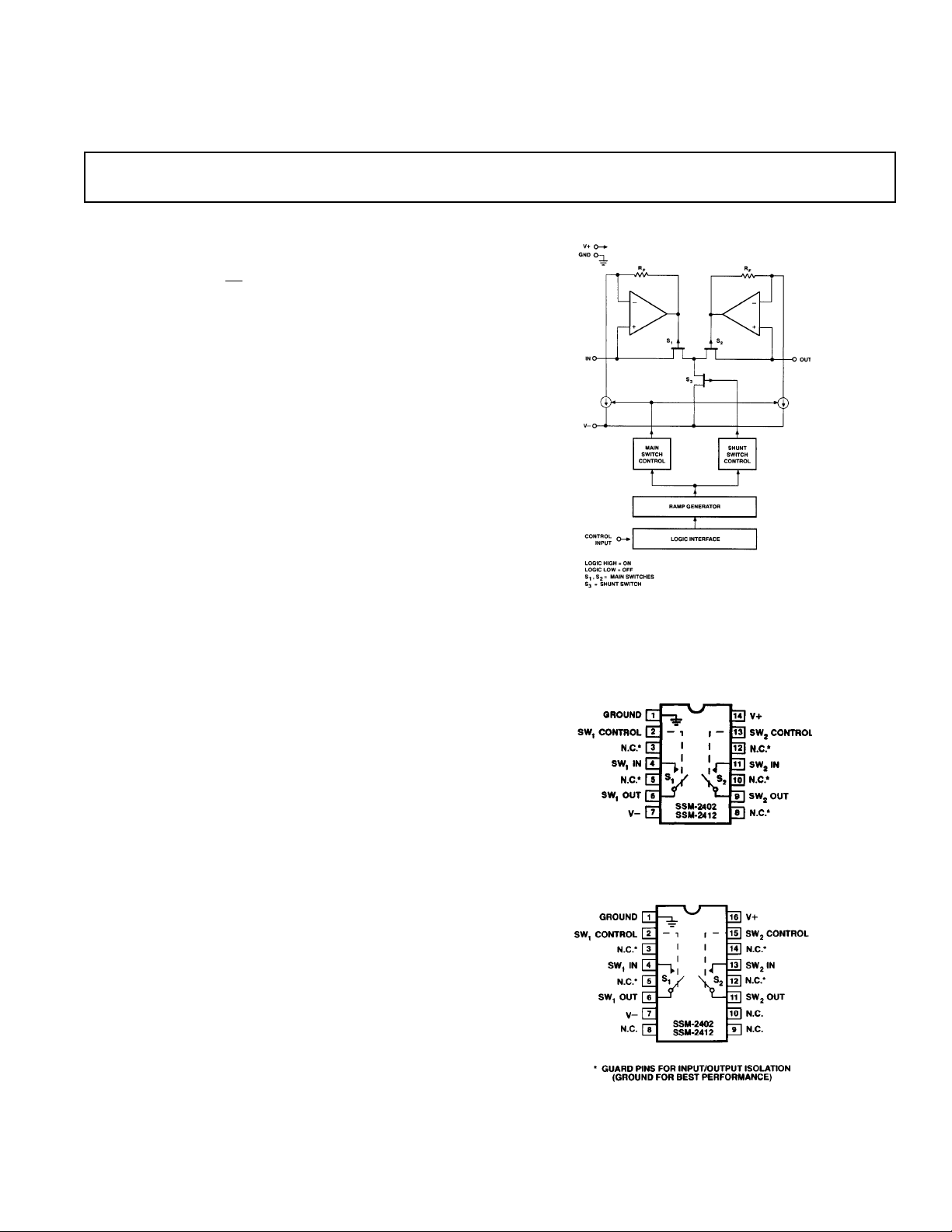
FUNCTIONAL BLOCK DIAGRAM
PIN CONNECTIONS
14-Pin Epoxy DIP
(P-Suffix)
16-Pin SOL
(S-Suffix)
REV. A
Information furnished by Analog Devices is believed to be accurate and
reliable. However, no responsibility is assumed by Analog Devices for its
use, nor for any infringements of patents or other rights of third parties
which may result from its use. No license is granted by implication or
otherwise under any patent or patent rights of Analog Devices.
One Technology Way, P.O. Box 9106, Norwood, MA 02062-9106, U.S.A.
Tel: 617/329-4700 Fax: 617/326-8703
Page 2

SSM2402/SSM2412–SPECIFICATIONS
ELECTRICAL CHARACTERISTICS
(@ VS = 618 V, RL = OPEN, and –408C ≤ TA ≤ +858C unless otherwise noted.
All specifications, tables, graphs, and application data apply to both the SSM2402 and SSM2412, unless otherwise noted.)
SSM2402/SSM2412
Parameter Symbol Conditions Min Typ Max Units
POSITIVE SUPPLY CURRENT +I
NEGATIVE SUPPLY CURRENT –I
GROUND CURRENT I
DIGITAL INPUT HIGH V
DIGITAL INPUT LOW V
LOGIC INPUT CURRENT I
ANALOG VOLTAGE RANGE
ANALOG CURRENT RANGE
3
3
SY
SY
GND
INH
INL
LOGIC
V
ANALOG
I
ANALOG
OVERVOLTAGE INPUT CURRENT VIN = ±V
SWITCH ON RESISTANCE R
ON
VIL = 0.8 V, 2.0 V
VIL = 0.8 V, 2.0 V
VIL = 0.8 V, 2.0 V
TA = Full Temperature Range 20 V
TA = Full Temperature Range 0.8 V
VIN = 0 V to 15 V
SUPPLY
–14.2 V ≤ VA ≤ +14.2 V
IA = ±10 mA, VIL = 2.0 V
T
= +25°C6085Ω
A
T
= Full Temperature Range 115 Ω
A
Tempco (∆RON/∆T) 0.2 Ω/°C
RON MATCH RON MATCH –14.2 V ≤ VA ≤ +14.2 V 1 5 %
IA = ±10 mA, VIL = 2.0 V
SWITCH ON LEAKAGE CURRENT I
S(ON)
VIL = 2.0 V
–14.2 V ≤ V
VA = 0 V 0.05 10.0 nA
SWITCH OFF LEAKAGE CURRENT I
S(OFF)
VIL = 0.8 V
–14.2 V ≤ V
VA = 0 V 0.05 10.0 nA
TURN-ON TIME
4
t
ON
VA = +10 V, RL = 2 kΩ SSM2402 10.0 ms
TA = +25°C, See Test Circuit SSM2412 3.5
TURN-OFF TIME
5
t
OFF
VA = +10 V, RL = 2 kΩ SSM2402 4.0 ms
TA = +25°C, See Test Circuit SSM2412 1.5
BREAK-BEFORE-MAKE t
TIME DELAY
6
OFF–tON
TA = +25°C SSM2402 6.0 ms
CHARGE INJECTION Q TA = +25°C SSM2402 50 pC
ON-STATE INPUT CS
(ON)
VA = 1 V rms 12 pF
CAPACITANCE f = 5 kHz, TA = +25°C
OFF-STATE INPUT CS
(OFF)
VA = 1 V rms 4 pF
CAPACITANCE f = 5 kHz, TA = +25°C
OFF ISOLATION I
SO(OFF)
VA = 10 V rms, 20 Hz to 20 kHz 120 dB
TA = +25°C, See Test Circuit
CHANNEL-TO-CHANNEL C
T
VA = 10 V rms, 20 Hz to 20 kHz 96 dB
CROSSTALK TA = +25°C
TOTAL HARMONIC THD 0 V to 10 V rms, 20 Hz to 20 kHz 0.003 0.01 %
DISTORTION
SPECTRAL NOISE DENSITY e
7
n
TA = +25°C, RL = 5 kΩ
20 Hz to 20 kHz, TA = +25°C 1 nV/√Hz
WIDEBAND NOISE DENSITY en p-p 20 Hz to 20 kHz, TA = +25°C 0.2 µV p-p
NOTES
1
“VIL” is the Logic Control Input.
2
Current tested at VIN = 0 V. This is the worst case condition.
3
Guaranteed by RON test condition.
4
Turn-ON time is measured from the time the logic input reaches the 50% point to the time the output reaches 50% of the final value.
5
Turn-OFF time is measured from the time the logic input reaches the 50% point to the time the output reaches 50% of the initial value.
6
Switch is guaranteed by design to provide break-before-make operation.
7
THD guaranteed by design and dynamic RON testing.
Specifications subject to change without notice.
1
1
1
2
6.0 7.5 mA
4.8 6.0 mA
0.6 1.5 mA
1.0 5.0 µA
–14.2 +14.2 V
–10 +10 mA
±40 mA
≤ +14.2 V 0.05 1.0 µA
A
≤ +14.2 V 0.05 1.0 µA
A
SSM2412 2.0
SSM2412 150
–2–
REV. A
Page 3
SSM2402/SSM2412
ABSOLUTE MAXIMUM RATINGS
Operating Temperature Range . . . . . . . . . . . –40°C to +85°C
Operating Supply Voltage Range . . . . . . . . . . . . . . . . . ±20 V
Analog Input Voltage Range
Continuous . . . . . . . . . . . . . . V– +3.5 V ≤ V
≤ V+ –3.5 V
A
Maximum Current Through Switch . . . . . . . . . . . . . . 20 mA
Logic Input Voltage Range . . . . . . . . . . . . V+ Supply to –2 V
V+ Supply to Ground . . . . . . . . . . . . . . . . . . . . . . . . . . +36 V
V– Supply to Ground . . . . . . . . . . . . . . . . . . . . . . . . . . . –20 V
V
to V– Supply . . . . . . . . . . . . . . . . . . . . . . . . . . . . . . +36 V
A
Package Type uJA* u
JC
Units
14-Pin Plastic DIP (P) 76 33 °C/W
16-Pin SOL (S) 92 27 °C/W
*θJA is specified for worst case mounting conditions, i.e., θJA is specified for device
in socket for P-DIP package; θJA is specified for device soldered to printed circuit
board for SOL package.
ORDERING GUIDE
Temperature Package
Model Range Description
SSM2402P –40°C to +85°C 14-Pin Plastic DIP
SSM2402S –40°C to +85°C 16-Pin SOL
SSM2412P –40°C to +85°C 14-Pin Plastic DIP
SSM2412S –40°C to +85°C 16-Pin SOL
DICE CHARACTERISTICS
Die Size 0.105 × 0.097 Inch, 10,185 sq. mils
(2.667 × 2.464 mm, 6.57 sq. mm)
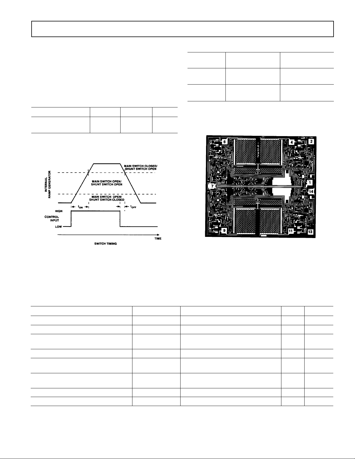
Timing Diagram
W AFER TEST LIMITS
Parameter Symbol Conditions
POSITIVE SUPPLY CURRENT +I
NEGATIVE SUPPLY CURRENT –I
GROUND CURRENT I
LOGIC INPUT CURRENT I
SWITCH ON RESISTANCE R
SY
SY
GND
LOGIC
ON
VIL = 0.8 V 7.5 mA max
VIL = 0.8 V 6.0 mA max
VIL = 0.8 V 1.5 mA max
VIN = 0 V
–14.2 V ≤ VA ≤ +14.2 V 85 Ω max
IA = ±10 mA, VIL = 2.0 V
MATCH BETWEEN SWITCHES RON MATCH –14.2 V ≤ VA ≤ +14.2 V 5 % max
R
ON
IA = ±10 mA, VIL = 2.0 V
SWITCH ON LEAKAGE CURRENT I
SWITCH OFF LEAKAGE CURRENT I
NOTES
1
VIL = Logic Control Input; VA = Applied Analog Input Voltage; IA = Applied Analog Input Current.
2
Worst Case Condition.
Electrical tests are performed at wafer probe to the limits shown. Due to variations in assembly methods and normal yield loss, yield after packaging is not
guaranteed for standard product dice. Consult factory to negotiate specifications based on dice lot qualifications through sample lot assembly and testing.
S(ON)
S(OFF)
–14.2 V ≤ VA ≤ +14.2 V, VIL = 2.0 V 1.0 µA max
–14.2 V ≤ VA ≤ +14.2 V, VIL = 0.8 V 1.0 µA max
1
2
Limit Units
5.0 µA max
REV. A
–3–
Page 4
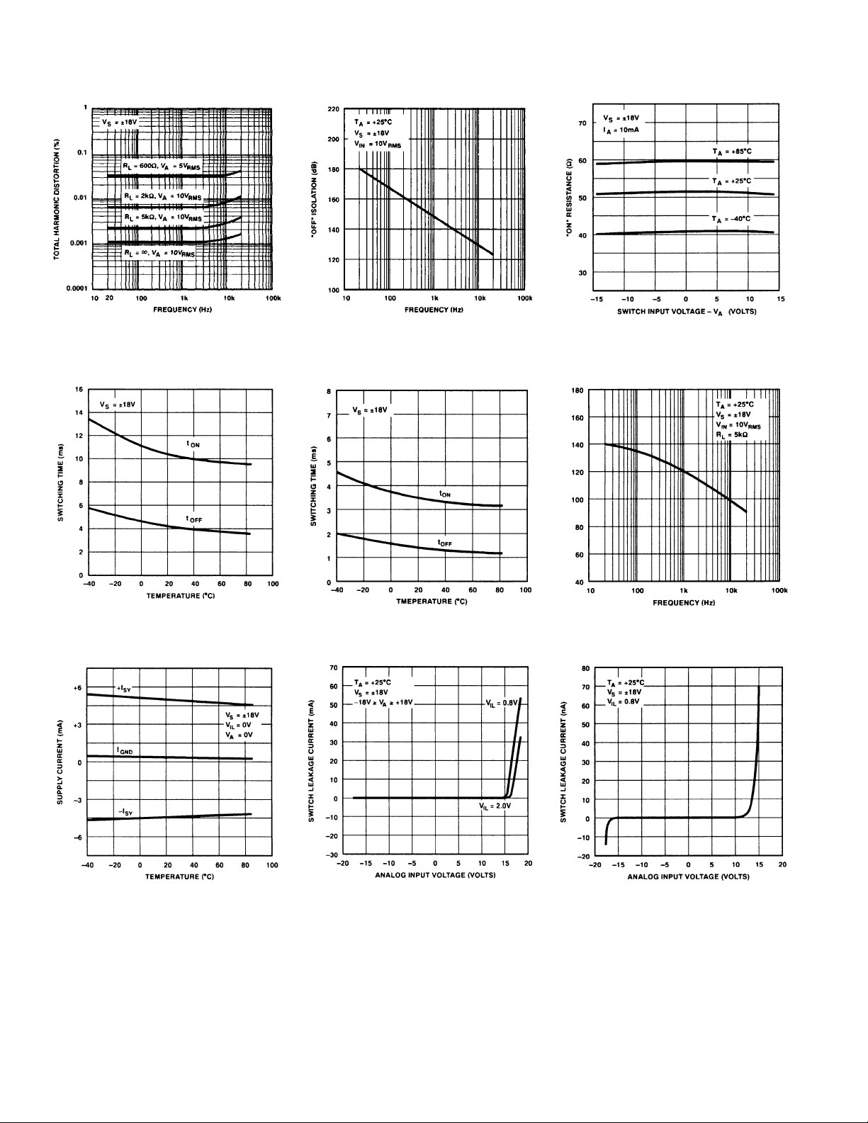
SSM2402/SSM2412–T ypical Performance Characteristics
Total Harmonic Distortion vs.
Frequency
SSM2402 Switching Time
vs. Temperature
“OFF” Isolation vs. Frequency
SSM2412 Switching Time
vs. Temperature
“ON” Resistance vs. Analog Voltage
Channel Separation vs. Frequency
Supply Current vs. Temperature
Overvoltage Characteristics
Leakage Current vs. Analog Voltage
REV. A–4–
Page 5

SSM2402/SSM2412
SSM2402 TON/T
SSM 2412 TON/T
Switching Response
OFF
Switching Response
OFF
TON/T
Switching Response Test Circuit
OFF
Switch ON/OFF Transition Test Circuit
REV. A
“OFF” Isolation Test Circuit
Switching ON/OFF Transition
–5–
Page 6

SSM2402/SSM2412
Switching Time Test Circuit
Simplified Schematic
–6–
REV. A
Page 7

APPLICATIONS INFORMATION
FUNCTIONAL SECTIONS
Each half of the SSM2402/SSM2412 are made up of three major
functional blocks:
1. “T” Switch
Consists of JFET switches S1 and S2 in series as the main
switches and switch S
2. Ramp Generator
as a shunt.
3
Generates a ramp voltage on command of the Control Input
(see Figure 1). A LOW-to-HIGH TTL input at Control
Input initiates a ramp that goes from approximately –7 V to
+7 V in 12 ms. Conversely, a HIGH-to-LOW TTL transition at Control Input will cause a downward ramp from approximately +7 V to –7 V in 12 ms for the SSM2402, and
4 ms for the SSM2412. The Ramp Generator also supplies
the +3 V and –3 V reference levels for Switch Control.
3. Switch Control
The ramp from the Ramp Generator section is applied to two
differential amplifiers (DA
and DA2) in the Switch Control
1
block. (See Simplified Schematic). One amplifier is referenced to –3 V and the other is referenced to +3 V. Switch
Control Outputs are:
—Main Switch Control—Drives two 0.25 mA current
sources that control the inverting inputs of each op amp.
When ON, the current sources cause a gate-to-source voltage of approximately 2.5 V which is sufficient to turn off
S
and S2. When the current sources from Main Switch
1
Control are OFF, each op amp acts as a unity-gain follower (V
= 0) and both switches (S1 and S2) will be ON.
GS
—Shunt Switch Control—Controls the Shunt Switch of
the “T” configuration.
SSM2402/SSM2412
Figure 1. Ramp Generator
SWITCH OPERATION
Unlike conventional analog switches, the SSM2402/SSM2412
are designed to ramp on and off gradually over several milliseconds. The soft transition prevents popping or clicking in audio
systems. Transients are minimized in active filters when the
SSM2402/SSM2412 are used to switch component values.
To see how the SSM2402/SSM2412 switches work, first consider an OFF-to-ON transition. The Control Input is initially
LOW and the Ramp Output is at approximately –7 V. The
Main Switch Control is HIGH which drives current sources Q
3
and Q4 to 0.25 mA each. These currents generate 2.5 V gateto-source back bias for each JFET switch (S
and S2) which
1
holds them OFF.
The Shunt Switch Control is negative which holds the shunt
JFET S
switches S
through S
ON. Undesired feedthrough signals in the series JFET
3
and S2 are shunted to the negative supply rail
1
.
3
Figure 2. Switch Control
When the Control Input goes from LOW to HIGH, the Ramp
Generator slews in the positive direction as shown in Figure 2.
When the ramp goes more positive than –3 V, the Shunt Switch
Control is pulled positive by differential amplifier DA
thereby puts shunt switch S
into the OFF state. Note that S
3
which
2
1
and S2 are still OFF, so at this time all three switches in the
“T” are OFF.
REV. A
–7–
Page 8

SSM2402/SSM2412
When the Ramp Output reaches +3 V, and the drive for the
Main Switch Control output is gated OFF by differential amplifier DA
V
, current sources Q3 and Q4 go to the OFF state and the
1
of each main switch goes to zero. The high speed op amp
GS
followers provide essentially zero gate-to-source voltage over the
full audio signal range; this in turn assures a constant low impedance in the ON state over the full audio signal range. Total
time to turn on the SSM2402 switch is approximately 10.0 ms
and 3.5 ms for the SSM2412.
In systems using a large number of separate switches, there are
advantages to having faster switching into OFF state than into
the ON state. Break-before-make can be maintained at the system level. To see how the SSM2402/SSM2412 guarantee
break-before-make, consider the ON-to-OFF transition.
A Control Input LOW initiates the ON-to-OFF transition. The
Ramp Generator integrates down from approximately +7 V towards –7 V. As the ramp goes through +3 V, the comparator
controlling the Main Switches (S
on current sources Q
and Q4 which thereby puts S1 and S2 into
3
and S2) goes HIGH and turns
1
the OFF state. At this time, all switches in the “T” are OFF.
When the ramp integrates down to –3 V, the Shunt Switch Control changes state and pulls shunt switch S
This completes the ON-to-OFF transition; S
and S
is ON to shunt away any undesired feedthrough. Note
3
though that the ON-to-OFF time for main switches S
into the ON state.
3
and S2 are OFF,
1
and S2 is
1
only the time interval required for the ramp to go from +7 V to
+3 V, about 4 ms for the SSM2402, and 1.5 ms for the
SSM2412. The time to turn on is about 2.5 times as long as the
time to turn off.
OVERVOLTAGE PROTECTION
The SSM2402/SSM2412 are designed to guarantee correct operation with inputs of up to ±14.2 V with ± 18 V supplies. The
switch input should never be forced to go beyond the supply
rails. In the OFF condition, if the inputs exceeds +14.2 V,
there is a risk of turning the respective input pass FET “ON.”
When the input voltage rises to within 3.8 V of the positive
supply, the op amp follower saturates and will not be able to
maintain the full 2.5 V of back bias on the gate-to-source
junction. Under this condition, current will flow from the input
through the shunt FET to the negative supply. This current is
substantial, but is limited by the FET I
. Although this cur-
DSS
rent will not damage the device, there is a danger of also turning on the output pass FET, especially if the output is close to
the negative rail.
This risk of signal “breakthrough” for inputs above +14.2 V can
be el i minated by using a source resistor of 100 Ω–500 Ω in series
with the analog input to provide additional current limiting.
Near the negative supply, transistors Q
and Q4 saturate and
3
can no longer keep the switch OFF. Signal breakthrough cannot happen, but the danger here is latch-up via a path to V–
through the shunt FET. Additional circuitry (not shown) has
been incorporated to turn OFF the shunt FET under these
conditions, and the potential for latch-up is thereby eliminated.
Typical Configuration
The SSM2402/SSM2412 are much more than simple single
solid state switches. The “T” configuration provides superb
OFF-isolation through shunting of feedthrough via shunt switch
S
. Break-before-make is inherent in the design. The ramp pro-
3
vides a controlled gating action that softens the ON/OFF transitions. Distortion is minimized by holding zero gate-to-source
voltage for the two main FET switches, S
and S2, using the two
1
op amp followers. Figure 3 shows a distortion comparison between the SSM2402 and a typical CMOS switch. In summary,
the SSM2402/SSM2412 are designed specifically for high performance audio system usage.
–8–
Figure 3. Comparison of the SSM2402 and
Typical CMOS Switch for Distortion
REV. A
Page 9

SSM2402/SSM2412
DIGITALLY-CONTROLLED ATTENUATOR
Figure 4 shows the usual approach to digitally-controlled attenuation. With S
output. With S
R
and R2. The advantage of this configuration is that the at-
1
closed, the signal passes unattenuated to the
1
open and S2 closed, the signal is attenuated by
1
tenuator current does not have to flow through the switches.
The disadvantage is that the output is undefined during the
switching period, which can be several milliseconds.
The low distortion characteristics of the SSM2402/SSM2412
enable the alternate arrangement of Figure 5 to be used. Now
only one switch is required to change between two gains, and
there is always a signal path to the output. Values for R
will
2
typically be in the low kilohm range.
For more gain steps and higher attenuation, the ladder arrange-
ment of Figure 6 can be used. This enables a wide dynamic
range to be achieved without the need for large value resistors,
which would result in degradation of the noise performance.
Figure 4.
Figure 5.
HIGH PERFORMANCE STEREO ROUTING SWITCHER
The SSM2402 Dual Audio Switch comprises the nucleus for
this 16 channels-to-one high performance stereo audio routing
switcher, which features negligible noise and low distortion over
the frequency range of 20 Hz to 20 kHz. This performance is
achieved even while driving 600 Ω loads at signal levels up to
+30 dBu.
The SSM2402 affords a much simplified electrical design and
printed circuit board layout, along with reduced manufacturing
cost, when compared with discrete JFET circuits of similar performance. The electrical performance of the design described is
vastly superior to CMOS switch designs, which are more prone
to failure resulting from electrical static discharge.
The switching control of the SSM2402 may be activated by
conventional mechanical switches or 5 volt TTL or CMOS logic
circuits. The application shown utilizes a simple mechanical
control switch for illustration purposes only. Many diverse X/Y
control schemes, destination control, or computer controlled
designs can be utilized.
The “T” configuration of the SSM2402 switch provides excellent ON-OFF isolation. The SSM2402 also features ms ramped
turn on and ms ramped turn off for click-free switching. Additionally, the switch has a break-before-make switching sequence.
Both features become significant in large audio switching systems where the audio path can pass through multiple switching
elements. Such controlled switching is very important in large
systems used in broadcast program switching or in production
work.
The application circuit design also employs the SSM2015 balanced input amplifier (Figure 7). The input impedance is high
(≈100 kΩ), balanced or unbalanced. The input circuit incorporates a single pole RFI filter with a cutoff frequency set at
145 kHz. In addition, the input circuit attenuates the signal by
25 dB and extends the common-mode input voltage range to
±98 volts peak, with common-mode rejection greater than
70 dB from 20 Hz to 20 kHz. The SSM2015 is set to produce a
15 dB gain. The signal drive level into the SSM2402 switch is
then +10 dBu with a +20 dBu input level and +14 dBu peak,
well within ideal operating range. Good signal-to-noise is maintained, with generous head-room available by electing to use
±18 V dc power supply voltages.
REV. A
Figure 6.
–9–
Page 10

SSM2402/SSM2412
Figure 7. Switcher Schematic
–10–
REV. A
Page 11

SSM2402/SSM2412
Figure 8. Switcher Functional Block Diagram
The routing switcher bus carries high level unbalanced audio,
but is driven with low impedance sources. With the output impedance of the SSM2015 at virtually 0 Ω and the SSM2402
switch ON, resistance is typically 60 Ω. Bus-to-bus crosstalk is
exceptionally low. For example, assuming 14 pF coupling between buses and 20 kHz signal, the crosstalk (isolation) exceeds
80 dB. The 14 pF would be representative for the 16 × 1 stereo
design shown. Shielding of the buses with a printed circuit
board ground plane and physically isolating the input and output circuits will reduce the crosstalk even further. The “T” configuration of the SSM2402 switch virtually eliminates crosstalk
between the various input signal sources.
The output amplifier incorporates a buffer amplifier that provides 4 dB of gain (nominally), with adjustable output level trim
control. The buffer also isolates the switching bus from the balanced output amplifier circuit. The balanced output is designed
to drive 600 Ω loads and utilizes two SSM2134 IC amplifiers.
The differential design increases drive capability, yet increases
the heat dissipation surface area, and keeps IC package temperature well within safe operating limits, even when driving
600 Ω loads. The SSM2134 is recommended due to its low
noise, wide frequency response, and output drive current
capabilities.
Overall performance of the 16 × 1 stereo switcher is noteworthy.
Input-to-output frequency response is flat to within 1 dB over a
10 Hz to 50 kHz band. Total harmonic distortion plus noise is
less than 0.03%, from 20 Hz to 20 kHz. SMPTE intermodulation distortion is less than 0.02%. The use of ± 18 V dc power
supplies produces a +30 dBm clip level, even when driving
600 Ω loads.
Table I. Circuit Performance Specifications
Max Input Level +30 dBu
Input Impedance, Unbalanced 100 kΩ
Input Impedance, Balanced 200 kΩ
Common-Mode Rejection (20 Hz to 20 kHz) >70 dB
Common-Mode Voltage Limit ±98 V Peak
Max Output Level +30 dBu/dBm
Output Impedance 67 Ω
Gain Control Range ±2 dB
Output Voltage Slew Rate 6 V/µs
Frequency Response (± 0.05 dB) 20 Hz to 20 kHz
Frequency Response (±0.5 dB) 10 Hz to 50 kHz
THD + Noise (20 Hz to 20 kHz, +8 dBu) 0.005%
THD + Noise (20 Hz to 20 kHz, +24 dBu) 0.03%
IMD (SMPTE 60 Hz & 4 kHz, 4:1, +24 dBu) 0.02%
Crosstalk (20 Hz to 20 kHz) >80 dB
S/N Ratio @ 0 dB Gain 135 dB
REV. A
–11–
Page 12

SSM2402/SSM2412
0.210 (5.33)
MAX
0.160 (4.06)
0.115 (2.93)
OUTLINE DIMENSIONS
Dimensions shown in inches and (mm).
14-Pin Epoxy DIP
(P-Suffix)
0.795 (20.19)
0.725 (18.42)
14
17
PIN 1
0.022 (0.558)
0.014 (0.356)
0.100
(2.54)
BSC
8
0.280 (7.11)
0.240 (6.10)
0.060 (1.52)
0.015 (0.38)
0.070 (1.77)
0.045 (1.15)
0.130
(3.30)
MIN
SEATING
PLANE
16-Pin SOL
(S-Suffix)
0.4133 (10.50)
0.3977 (10.00)
0.325 (8.25)
0.300 (7.62)
0.015 (0.381)
0.008 (0.204)
0.195 (4.95)
0.115 (2.93)
0.0118 (0.30)
0.0040 (0.10)
16 9
PIN 1
0.0500
0.0192 (0.49)
(1.27)
0.0138 (0.35)
BSC
0.2992 (7.60)
81
0.1043 (2.65)
0.0926 (2.35)
SEATING
PLANE
0.2914 (7.40)
0.4193 (10.65)
0.3937 (10.00)
0.0125 (0.32)
0.0091 (0.23)
0.0291 (0.74)
0.0098 (0.25)
0.0500 (1.27)
8°
0°
0.0157 (0.40)
x 45°
–12–
PRINTED IN U.S.A.
REV. A
 Loading...