

Page 1
SW1 A
SW1 B
DGND
SW1 CONTROL
SW2 CONTROL
NC
*
SW2 B
SW2 A
SW4 A
SW4 B
V+
SW4 CONTROL
SW3 CONTROL
V–
SW3 B
SW3 A
NC = NO CONNECT
AGND
AGND
AGND
AGND
*
CONNECT TO ANALOG GROUND
FOR BEST NOISE ISOLATION
SW1
1
2
3
4
5
6
7
8
20
19
18
17
16
15
14
13
9
10
12
11
TOP VIEW
(Not to Scale)
O
SSM2404
SW1
SW2 SW3
SW4
a
Quad Audio Switch
SSM2404
FEATURES
“CIickless” Bilateral Audio Switching
Four SPST Switches in a 20-Pin Package
Ultralow THD+N: 0.0008% @ 1 kHz (2 V rms,
= 100 kV)
R
L
Low Charge Injection: 35 pC typ
High OFF Isolation: –100 dB typ (RL = 10 kV @ 1 kHz)
Low Crosstalk: –94 dB typ (R
= 10 kV @ 1 kHz)
L
Low ON Resistance: 28 V typ
Low Supply Current: 900 mA typ
Single or Dual Supply Operation: +11 V to +24 V or
65.5 V to 612 V
Guaranteed Break-Before-Make
TTL and CMOS Compatible Logic Inputs
Low Cost-Per-Switch
GENERAL DESCRIPTION
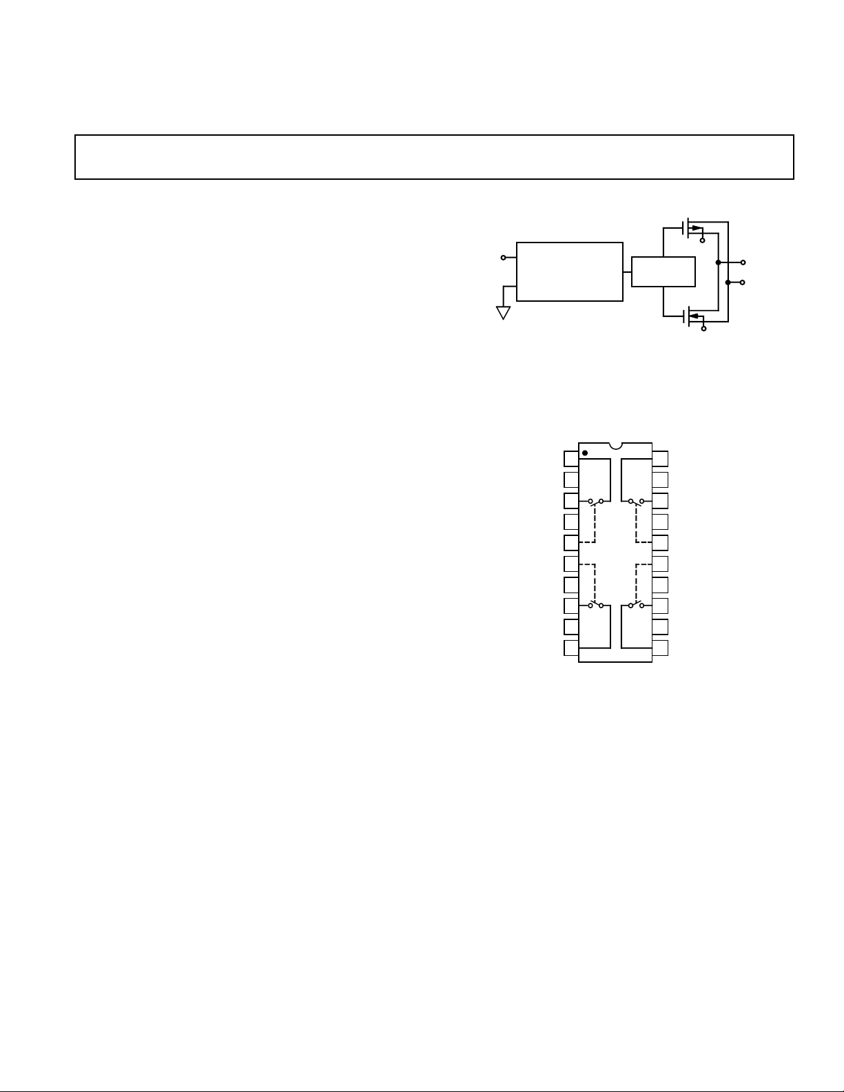
The SSM2404 integrates four SPST analog switches in a single
20-pin package. Developed specifically for high performance
audio applications, distortion and noise are negligible over the
full operating range of 20 Hz to 20 kHz. With very low charge
injection of 35 pC, “clickless” audio switching is possible, even
under the most demanding conditions.
Switch control is realized by conventional TTL or CMOS
logic. Guaranteed “break-before-make” operation assures that
all switches in a large system will open before any switch
reaches the ON state.
Single or dual supply operation is possible. Additional features
include –100 dB OFF isolation, –94 dB crosstalk and 28 Ω ON
resistance. Optional current-mode switching permits an
extended signal-handling range. Although optimized for large
load impedances, the SSM2404 maintains good audio
performance even under low load impedance conditions.
BLOCK DIAGRAM OF ONE SWITCH CHANNEL
CONTROL
DIGITAL
CONTROL
LOGIC INTERFACE
AND
BREAK-BEFORE-MAKE
CONTROL
RAMP
GENERATOR
V–
V+
PIN CONNECTIONS
Epoxy Mini-DIP (P Suffix)
and SOIC (S Suffix)
SW1 A
SW1 B
REV. B
Information furnished by Analog Devices is believed to be accurate and
reliable. However, no responsibility is assumed by Analog Devices for its
use, nor for any infringements of patents or other rights of third parties
which may result from its use. No license is granted by implication or
otherwise under any patent or patent rights of Analog Devices.
One Technology Way, P.O. Box 9106, Norwood, MA 02062-9106, U.S.A.
Tel: 617/329-4700 Fax: 617/326-8703
Page 2
(VS = 612 V, TA = +258C, unless otherwise noted.
SSM2404–SPECIFICATIONS
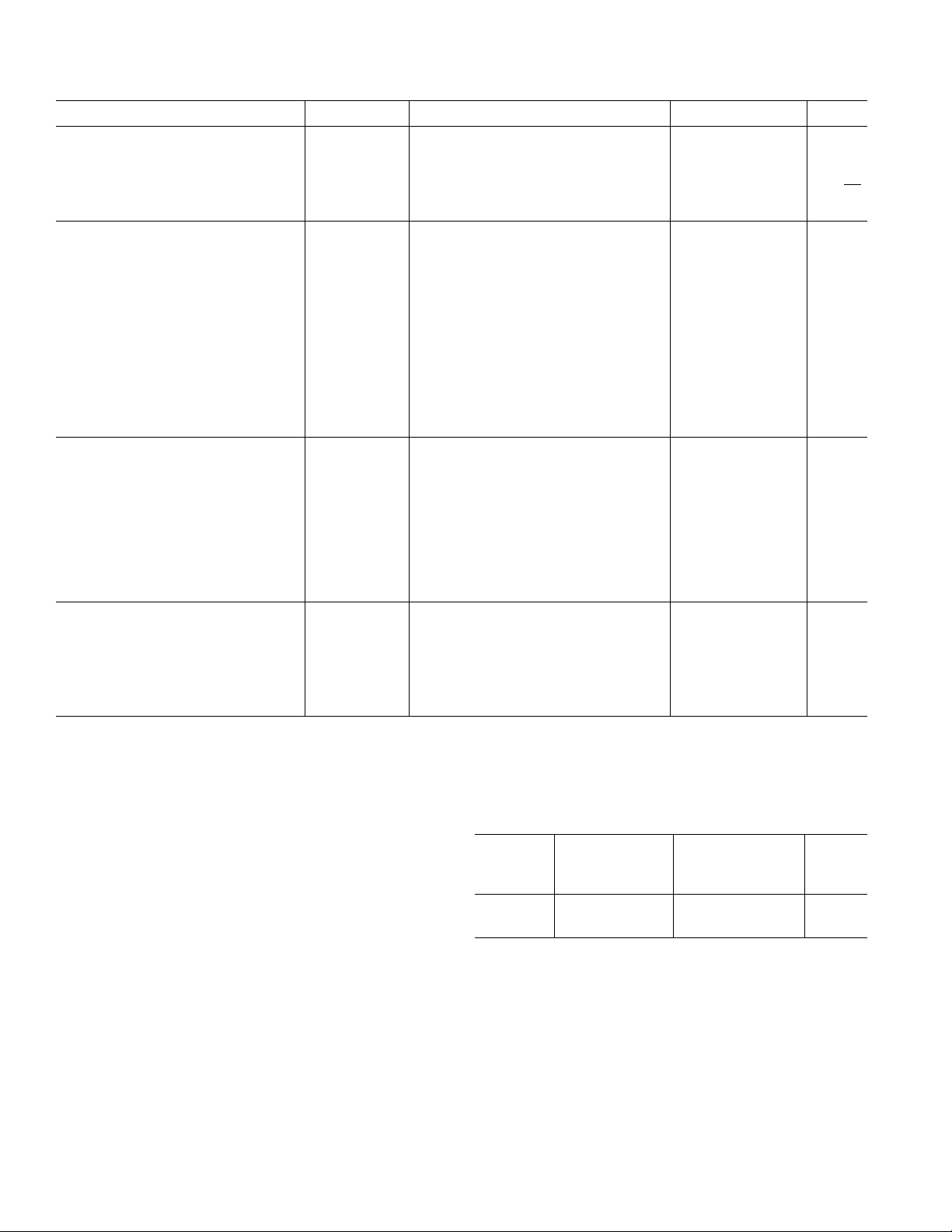
Parameter Symbol Conditions Min Typ Max Units
AUDIO PERFORMANCE
Total Harmonic Distortion Plus Noise THD+N @ 1 kHz, with 80 kHz Filter,
Spectral Noise Density e
Wideband Noise Density en p-p 20 Hz to 20 kHz 0.6 µV p-p
ANALOG SIGNAL SECTION
Analog Voltage Range V
Analog Current Range I
ON Resistance R
Matching RON Match IA = ±10 mA, VA = 0 V 1 %
R
ON
ON Leakage Current I
OFF Leakage Current I
Charge Injection Q 35 pC
ON-State Input Capacitance C
OFF-State Input Capacitance C
OFF Isolation I
Channel-to-Channel Crosstalk C
CONTROL SECTION
Digital Input High V
Digital Input Low V
Turn-On Time
Turn-Off Time
1
2
Break-Before-Make Time Delay t
Logic Input Current
Logic HI V
Logic LO V
POWER SUPPLY
Supply Voltage Range V
Positive Supply Current I
Negative Supply Current I
Ground Current All Channels On –2.0 –0.3 mA
NOTES
1
Turn-on time is measured from the time the logic input reaches the 50% point to the time the output reaches 50% of the final value.
2
Turn-off time is measured from the time the logic input reaches the 50% point to the time the output reaches 50% of the initial value.
Specifications subject to change without notice.
n
A
A
ON
S(ON)
S(OFF)
ON
OFF
SO(OFF)
T
INH
INL
t
ON
t
OFF
ON-tOFF
S
SY+
SY–
Typical specifications apply at TA = +258C.)
= 100 kΩ, VIN = 2 V rms 0.0008 %
R
L
20 Hz to 20 kHz 0.8 nV/√Hz
V
= 2.4 V, IA = ±2 mA ±12 V
INH
V
= 2.4 V, VA = 0 V ±10 mA
INH
IA = ±10 mA, VA = ±10 V dc 28 45 Ω
VA = ±10 V –20 0.1 +20 nA
VA = ±10 V –20 0.1 +20 nA
VA = 5 V rms 31 pF
VA = 5 V rms 17 pF
VA = 50 mV rms, f = 1 kHz, RL = 10 kΩ –100 dB
VA = 50 mV rms, f = 1 kHz, RL = 10 kΩ –94 dB
DGND = 0 V 2.4 V
DGND = 0 V 0 0.8 V
See Test Circuit 8 50 ms
See Test Circuit 5 30 ms
320ms
= 2.4 V –1000 1.3 +1000 nA
INH
= 0.8 V –1000 1.0 +1000 nA
INL
Single Supply +11 +24 V
Dual Supply ±5.5 ±12 V
All Channels On 0.9 5 mA
All Channels On –1.5 –0.6 mA
V
S
ABSOLUTE MAXIMUM RATINGS
Supply Voltage
Single Supply . . . . . . . . . . . . . . . . . . . . . . . . . . . . . . .+27 V
Dual Supply . . . . . . . . . . . . . . . . . . . . . . . . . . . . . . ±13.5 V
Analog Input Voltage (V
Logic Input Voltage (V
) . . . . . . . . . . . . . . . . . . . . . . . . . .V
A
) . . . . . . . . . . . . . . . . . . . . . . V
INL/INH
Maximum Current Through Any Switch . . . . . . . . . . . 20 mA
Operating Temperature Range . . . . . . . . . . . . –40°C to +85°C
Storage Temperature Range . . . . . . . . . . . . –65°C to +150°C
Junction Temperature (T
Lead Temperature (Soldering, 60 sec) . . . . . . . . . . . . +300°C
Thermal Resistance
) . . . . . . . . . . . . . . . . . . . . +150°C
J
1
20-Pin Plastic DIP (P): θJA = 74, θJC = 32 . . . . . . . . . °C/W
20-Pin SOIC (S): θ
NOTE
1
θJA is specified for worst case mounting conditions, i.e., θJA is specified for device
in socket for P-DIP package.
= 90, θJC = 27 . . . . . . . . . . . . . . °C/W
JA
ORDERING GUIDE
Operating
Temperature Package
Model Range Package Option*
S
S
SSM2404P –40°C to +85°C 20-Pin Plastic DIP N-20
SSM2404S –40°C to +85°C 20-Pin SOIC R-20
*N = Plastic DIP, R = SOIC.
–2–
REV. B
Page 3
V = 50mV
0.01
0.001
0.0001
0 ±12±8±4
SUPPLY VOLTAGE – V
THD + N – %
A (IN) RMS
f = 20Hz TO 100kHz
V
50Ω
A (IN)
R = 10kΩ AND 100kΩ
V
OFF ISOLATION = 20 LOG
A (OUT)
V
A (IN)
OFF Isolation Test Circuit
SSM2404
V
A (OUT)
L
LOGIC
INPUT
V
A (IN)
V
A (OUT)
V
A (IN)
CONROL
Test Circuit for tON/t
HIGH
100ns
1.4V
LOW
DC VOLTAGE
OPEN OPEN
tON/t
SWITCH
t
r
100ns
t
f
CLOSED
50%
t
ON
Timing Diagram
OFF
+12V
V+
GND
V–
–12V
Timing Specification, tON/t
OFF
1.4V
V
A (OUT)
LOW
50%
t
OFF
OFF
Switching Response, and ON/OFF Transition Photos
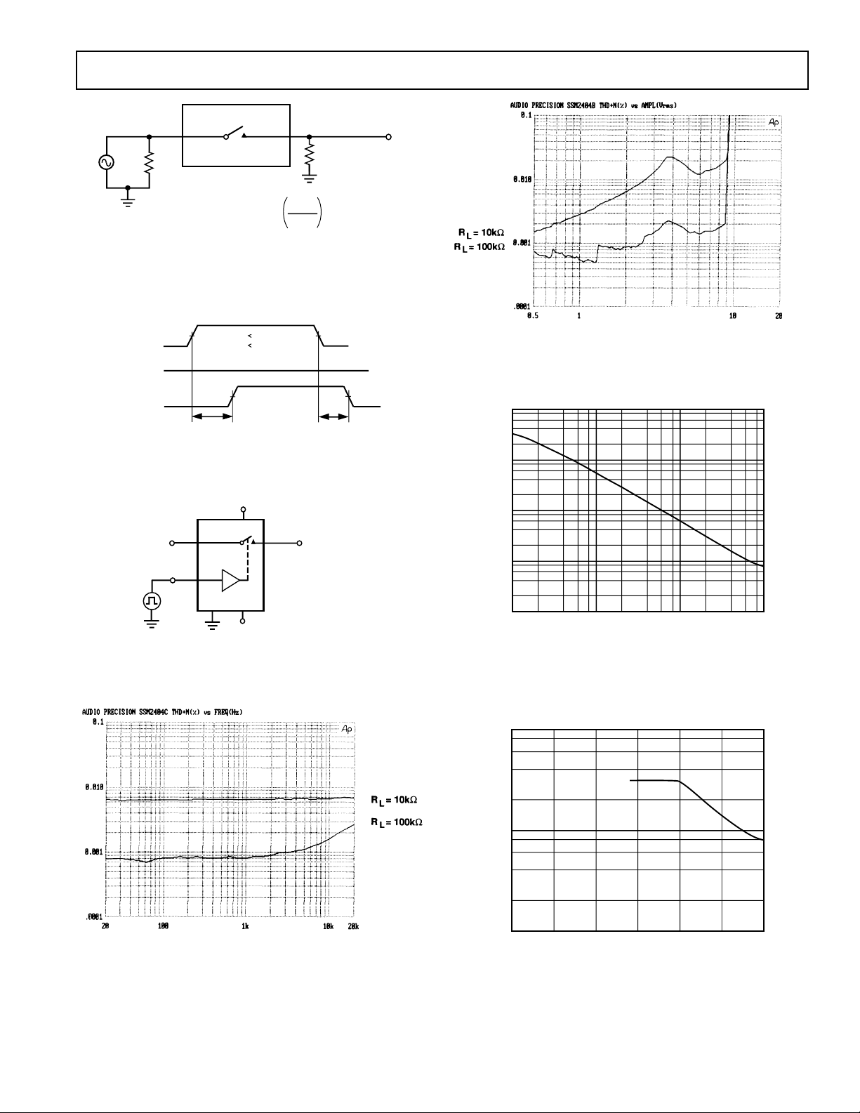
Figure 2. Headroom (VS = ±12 V, f = 1 kHz, with
80 kHz Filter)
1.0
0.1
0.01
THD + N – %
0.001
0.0001
100 1k 100k10k
LOAD RESISTANCE – Ω
Figure 3. THD+N vs. Load (VS = ±12 V, VA = 2 V rms,
f = 1 kHz, with 80 kHz Filter)
Figure 1. THD+N vs. Frequency (VS = ±12 V,
= 2 V rms, with 80 kHz Filter)
V
A
REV. B
Figure 4. THD+N vs. Supply Voltage (VA = 2 V rms,
f = 1 kHz, R
= 100 kΩ, with 80 kHz Filter)
L
–3–
Page 4

SSM2404
Figure 5. Frequency Response (VS = ±12 V,
V
= 1 V rms, RL = 100 kΩ)
A
CH A: 8.00µV FS 1.00µV/DIV
MKR: 20 000Hz
Figure 6. SSM2404 Spectral Noise Density e
[5 Devices (20 Switches) Chained Together]
100
90
0V
10
0V
0%
Figure 7. Square Wave Response (TA = +25°C,
= ±12 V, RL = 100 kΩ, f = 20 kHz)
V
S
10V
10V
0Hz
MKR: 0.11µV/ Hz
25kHz
BW: 150Hz
5µs
n
INPUT
OUTPUT
9.5
9.0
RMS
8.5
8.0
7.5
7.0
OUTPUT VOLTAGE SWING – V
6.5
6.0
100 1k 100k10k
LOAD RESISTANCE – Ω
T = 25°C
A
V = ±12V
S
f = 20kHz
Figure 8. Output Voltage Swing vs. Load Resistance
10
9
8
RMS
7
T = 25°C
6
5
4
3
2
OUTPUT VOLTAGE SWING – V
1
0
±4
±6
SUPPLY VOLTAGE – Volts
±8
A
R = 100kΩ
L
f = 20kHz
0.1% THD + N
±10
±12
Figure 9. Output Voltage Swing vs. Supply Voltage
–20
–30
–40
–50
–60
–70
–80
OFF ISOLATION – dB
–90
–100
–110
–120
100 100k10k1k10
FREQUENCY – Hz
T = 25°C
A
V = ±12V
S
V = 50mV
A
R = 100k
L
R = 10k
RMS
L
Figure 10. OFF-Isolation vs. Frequency
–4–
REV. B
Page 5

SSM2404
50
–20
10
–10
–5
0
–10
40
20
30
1050
V = ±12V
V = 0.8V
R =
∞
S
INL
L
–40°C TO +85°C
ANALOG INPUT VOLTAGE – Volts
SWITCH LEAKAGE CURRENT – nA
20
0
100
6
2
–20
4
–40
12
8
10
14
16
18
806040200
TEMPERATURE – °C
SWITCHING TIME – ms
V = ±12V
V = ±5V
R =
∞
S
A
L
T
ON
T
OFF
1.0
–1.0
100
–0.4
–0.8
–20
–0.6
–40
0.2
–0.2
0
0.4
0.6
0.8
806040200
TEMPERATURE – °C
SUPPLY CURRENT – mA
I
SY+
I
SY–
I
GND
V = ±12V
V = GND
V = 2.4V
S
A
INH
0
–15
–30
–45
–60
–75
–90
CROSSTALK – dB
–105
–120
–135
–150
100 100k10k1k10
R = 100k
L
FREQUENCY – Hz
T = 25°C
A
V = ±12V
S
V = 50mV
A
R = 10k
L
RMS
Figure 11. Channel-to-Channel Crosstalk vs. Frequency
(Worst Case Conditions, as Measured Between
Switches 1 and 4, or 2 and 3)
50
V = ±12V
S
∞
R =
40
30
L
I = 10mA
A
+85°C
+25°C
Figure 14. Leakage Current vs. Analog Voltage
20
ON RESISTANCE – Ω
10
0
–10
Figure 12. ON Resistance vs. Analog Voltage
90
80
70
60
50
40
30
20
10
0
SWITCH LEAKAGE CURRENT – mA
–10
–20
–15
Figure 13. Overvoltage Characteristics
REV. B
ANALOG INPUT VOLTAGE – Volts
–10
ANALOG INPUT VOLTAGE – Volts
0
T = 25°C
A
V = ±12V
S
R =
∞
L
5
1050–5
–40°C
V = 0.8V
IL
10–5
V = 2.4V
IH
15
Figure 15. Switching Time vs. Temperature
Figure 16. Supply Current vs. Temperature
–5–
Page 6

SSM2404
10V
5V
0
5V
0
Figure 17. tON/t
OPEN
(SWITCH OFF)
SSM2404 can also be configured as a 4:1 multiplexer, or by
100
90
ANALOG
OUTPUT
V
A (OUT)
using additional packages, as 8:1 or 16:1 and up. The breakbefore-make feature is guaranteed from part to part allowing
such multiple-package applications.
As Figure 20 shows, the SSM2404 is easy to use, and no additional devices are needed. The load resistors are recommended
10
0%
5ms/div
Switching Response
OFF
100
90
10
0%
50mV
50µs
LOGIC
INPUT
V
INL/INH
CLOSED
(SWITCH ON)
for improved OFF-isolation and charge injection. The ON
resistance of the switch is only 28 Ω typically, which causes very
little signal attenuation even with a load resistor.
IN1
R
L
OUT1
DGND
SW1 CONTROL
SW2 CONTROL
OUT2
R
IN2
L
1
2
SW1 SW4
3
4
TOP VIEW
5
(Not to Scale)
SSM2404
6
7
8
9
SW2 SW3
10
R IS OPTIONAL
L
20
19
18
17
16
15
14
13
12
11
IN4
R
L
OUT4
+12V
SW4 CONTROL
SW3 CONTROL
–12V
OUT3
R
L
SW
CONTROL
IN3
0
1
SWITCH
STATE
OFF
ON
Figure 18. Switch OFF-to-ON Transition (RL = 5 kΩ)
100
90
CLOSED
(SWITCH ON)
10
0%
50mV
50µs
OPEN
(SWITCH OFF)
Figure 19. Switch ON-to-OFF Transition (RL = 5 kΩ)
APPLICATIONS INFORMATION
The SSM2404 integrates four analog CMOS switches with
guaranteed “break-before-make” operation to provide high
quality audio switching. Each switch has complementary
N-channel and P-channel MOSFETs to allow the analog input
voltage range to include the positive and negative rails and
improve linearity. In addition, the topology permits fully
bilateral switching. When using the SSM2404 there is full
flexibility in configuring the switches. For example, they can be
used individually as shown in Figure 20, or as a double-pole,
double-throw (DPDT) switch, which is explained later. The
Figure 20. Basic Circuit Configuration
OPTIMIZING PERFORMANCE
As the performance curves show, the switch is optimized for
high impedance loads. The distortion performance is at its best
when the switch has a load impedance of 100 kΩ or greater as
shown in Figure 1. However, even at lower values of load resistances, the 1 kHz distortion performance is still excellent,
0.006% for a 10 kΩ load. The main trade-off with THD is
OFF-isolation and crosstalk. This is shown in Figures 10 and
11, again with two different load conditions. As these graphs
show, the 10 kΩ load yields approximately a 16 dB improvement in both characteristics.
Thus, the optimum operating point depends on the most critical parameters. When THD is critical then high load impedances should be used; however, when crosstalk and OFFisolation are critical, lower impedances on the order of 10 kΩ
should be used. An additional benefit of using the smaller
load resistor is that any charge injected onto the output will be
shunted to ground through the resistor. If improved OFFisolation is needed, the SSM2404 dual audio switch should be
considered with its excellent 120 dB OFF-isolation at 20 kHz.
It is important that all of the AGND pins be connected to the
system analog ground. These pins isolate the input and output
of each switch. Without connecting these pins, the OFFisolation will degrade significantly.
–6–
REV. B
Page 7

SSM2404
DETAILED SWITCH OPERATION
A simplified circuit schematic with the functional sections is
shown in Figure 21. The TTL interface has an internally
regulated 5 V to ensure TTL logic levels regardless of the supply
voltage. The logic threshold is with respect to the DGND pin,
which can be offset. For example, if DGND is connected to the
negative supply, then the SSM2404 will operate with negative
rail logic. The interface shifts the control logic down to the
negative supply and inverts it to drive N1.
V+
100nA
P3
P2
N2
RAMP GENERATOR
SW1 A
BIAS
N4 P4
–1
C2
15pF
–1
N3
SW1 B
V–
SW
CONTROL
DGND
TTL
INTERFACE
100nA
C1
15pF
N1
BREAK-BEFORE-MAKE
P1
Figure 21. Simplified Schematic
N1 in combination with C1 and the 100 nA current source
provides the break-before-make operation of the switch. When
the switch is on, N1 is off and C1 is charged up to the positive
rail. However, when the SW CONTROL is turned off, then the
gate of N1 is pulled high. This turns N1 on, providing a low
impedance path to quickly discharge C1 to the negative rail,
which quickly “breaks” the switch. On the other hand, when the
SW CONTROL goes high again, the gate of N1 is pulled low,
turning it off. This leaves C1 to be slowly charged up to the
positive rail by the 100 nA current source. The difference in the
discharge and charging times ensures break-before-make
operation, even from device to device.
The voltage on C1 is inverted by P1 to drive the ramp generator
differential pair, consisting of P2, P3 and N2, N3. This differential pair steers the 100 nA of tail current to either charge or
discharge C2. As discussed above, when the switch is on, C1 is
charged up to the positive rail. P1 inverts this, putting a low
voltage equivalent to the negative supply on the gate of P2. The
BIAS voltage is approximately equal to the midpoint of the two
supply voltages. Thus, when P2 is pulled down, it is turned on
and P3 is off. All of the 100 nA flows through N2 and is mirrored by N3. Thus, the 100 nA discharges C2 through N3.
When C2 is pulled low, the inverter turns N4 on by pulling its
gate high, and the second inverter turns P4 on. To turn the
switch off the gate of P2 is pulled above the BIAS so that all
100 nA charges C2 through P3. This is then inverted to turn off
N4 and P4.
The internal ramp has rise and fall times on the order of a few
milliseconds which is sped up by the inverters. As the gate
voltages of N4 and P4 are changing, the ON resistance of each
switch is ramping from its OFF state to 28 Ω and vice versa.
The actual rise and fall times are shown in Figures 18 and 19
for a 5 kΩ load. These times are significantly slower than
typical switches, minimizing the SSM2404’s charge injection
and giving it “clickless” performance.
DOUBLE-POLE DOUBLE-THROW SWITCH
The SSM2404 is ideal as a one-chip solution for a stereo
switch. The schematic in Figure 22 shows the typical configuration. This circuit will select one of two stereo sources, channel
A or B. The switch controls for the left and right input of each
channel are tied together so that both will be turned on or off
simultaneously. An inverter is inserted between the channel A
and B controls so that only one logic signal is needed. The outputs can be configured many different ways, such as an inverting or noninverting amplifier stage, and the 10 kΩ load resistors
are added to improve the OFF-isolation. The performance of
this stereo switch is equivalent to each individual switch, yielding a high quality audio switch that is virtually transparent to
the signal.
V+
17
SSM2404
SWA/SWB
10 8
L
INA
13
L
INB
6
15
4
5
16
11
R
INA
20
R
INB
SW2
SW1
SW2 CONTROL
SW3 CONTROL
DGND
SW1 CONTROL
SW4 CONTROL
SW3
SW4
AGND
14
V–
L
OUT
10kΩ
2
9
12
19
SWA/SWB
13
18
10kΩ
0
1
R
OUT
CHANNEL
SELECTED
B
A
Figure 22. Double-Pole, Double-Throw Stereo Switch
VIRTUAL GROUND SWITCHING
The SSM2404 was built on a CMOS process with a 24 V
operating limit for the total supply voltage across the part. This
leads to a corresponding limit on the analog voltage range. However, to achieve larger signal swings, the SSM2404 should be
configured in the virtual ground mode. As shown in Figure 23,
the output of the SSM2404 is connected to the inverting input
of an amplifier. Since the noninverting input is grounded, the
SSM2404 will also be biased at ground, and large voltage
swings on the circuit’s input will not significantly change the
voltage on the switch. The only limitation is that the current
through the switch needs to be less than ±10 mA, and the voltage
range is limited only by the op amp and its supply voltages.
REV. B
–7–
Page 8

SSM2404
L
INA
L
INB
SW2
SW1
SW2 CONTROL
SW3 CONTROL
DGND
SW1 CONTROL
SW4 CONTROL
R
INA
SW3
SW4
AGND
SSM2404
V–
SWA/SWB
V+
17
10
8
13
2
R
OUT
9
12
19
13
18
14
20
11
16
5
4
15
6
5k
L
OUT
SSM2131
SSM2131
5k
5k
5k
R
INB
5k
5k
Ω
Ω
Ω
Ω
Ω
Ω
0.0500 (1.27)
BSC
0.0192 (0.49)
0.0138 (0.35)
0.0118 (0.30)
0.0040 (0.10)
0.0500 (1.27)
0.0157 (0.40)
0.1043 (2.65)
0.0926 (2.35)
0.0125 (0.32)
0.0091 (0.23)
0.4193 (10.65)
0.3937 (10.00)
0.2992 (7.60)
0.2914 (7.40)
0.5118 (13.00)
0.4961 (12.60)
110
20 11
PIN 1
0
°- 8°
0.0291 (0.74)
0.0098 (0.25)
X
45
°
The circuit was tested with an SSM2131 high slew rate audio
amplifier and the results are shown in Figures 24 and 25. This
configuration yields excellent THD performance that is
primarily determined by the amplifier. Also, the headroom is
now +24 dBu (0 dBu = 0.775 V rms), which is due to the
amplifier’s output voltage swing. Thus, even though the
SSM2404 has a ±12 V limitation on its supplies, it can be used
in systems with much higher voltage ranges. For example, the
double-pole double-throw switch from Figure 22 can be
reconfigured in the virtual ground mode to allow higher voltage
swings, as shown in Figure 26. This application realizes the
excellent performance of Figures 24 and 25 while providing a
low cost switching solution.
C1626–20–1/92
AUDIO
1N914
+12V
SSM2404
R1
5kΩ
IN
SW1 A
13
SW1 B
–12V
R2
5kΩ
+18V
SSM2131
–18V
AUDIO
OUT
Figure 23. Virtual Ground Switching
Figure 24. Virtual Ground Switch THD+N vs. Frequency
(V
= ±12 V, VA = 2 V rms, with 80 kHz Filter)
S
Figure 26. Double-Pole, Double-Throw Stereo Switch
Using Virtual Ground Operation
OUTLINE DIMENSIONS
Dimensions shown in inches and (mm).
Mini-DIP (P Suffix)
PIN 1
0.210
(5.33)
MAX
0.200 (5.05)
0.125 (3.18)
20
1
0.022 (0.558)
0.014 (0.356)
1.060 (26.90)
0.925 (23.50)
0.100 (2.54)
BSC
11
10
0.070 (1.77)
0.045 (1.15)
0.280 (7.11)
0.240 (6.10)
0.060 (1.52)
0.015 (0.38)
0.150
(3.81)
MIN
SEATING
PLANE
0.325 (8.25)
0.300 (7.62)
0.015 (0.381)
0.008 (0.204)
0.195 (4.95)
0.115 (2.93)
Figure 25. Virtual Ground Switch Headroom (VS = ±12 V
for SSM2404; V
80 kHz Filter)
= ±18 V for Op Amp, f = 1 kHz, with
S
–8–
SOIC (S Suffix)
PRINTED IN U.S.A.
REV. B
 Loading...