

Page 1
Low Distortion, 1.5 W Audio
www.BDTIC.com/ADI
FEATURES
1.5 W output with THD + N < 1%
Differential bridge-tied load output
Single-supply operation: 2.7 V to 5.5 V
Functions down to 1.75 V
Wide bandwidth: 4 MHz
Highly stable phase margin: >80°
Low distortion: 0.2% THD + N @ 1 W output
Excellent power supply rejection
APPLICATIONS
Portable computers
Personal wireless communicators
Hands-free telephones
Speaker phones
Intercoms
Musical toys and talking games
GENERAL DESCRIPTION
The SSM22111 is a high performance audio amplifier that
delivers 1 W rms of low distortion audio power into a bridgeconnected 8 Ω speaker load (or 1.5 W rms into a 4 Ω load).
The SSM2211 operates over a wide temperature range and is
specified for single-supply voltages between 2.7 V and 5.5 V.
When operating from batteries, it continues to operate down to
1.75 V. This makes the SSM2211 the best choice for unregulated
applications, such as toys and games.
Featuring a 4 MHz bandwidth and distortion below 0.2% THD
+ N @ 1 W, superior performance is delivered at higher power
or lower speaker load impedance than competitive units.
Furthermore, when the ambient temperature is at 25°C, THD +
N < 1%, and V
delivers a 1.5 W output.
1
Protected by U.S. Patent No. 5,519,576.
Rev. E
Information furnished by Analog Devices is believed to be accurate and reliable. However, no
responsibility is assumed by Analog Devices for its use, nor for any infringements of patents or other
rights of third parties that may result from its use. Specifications subject to change without notice. No
license is granted by implication or otherwise under any patent or patent rights of Analog Devices.
Trademarks and registered trademarks are the property of their respective owners.
= 5 V on a four-layer PCB, the SSM2211
S
Power Amplifier
SSM2211
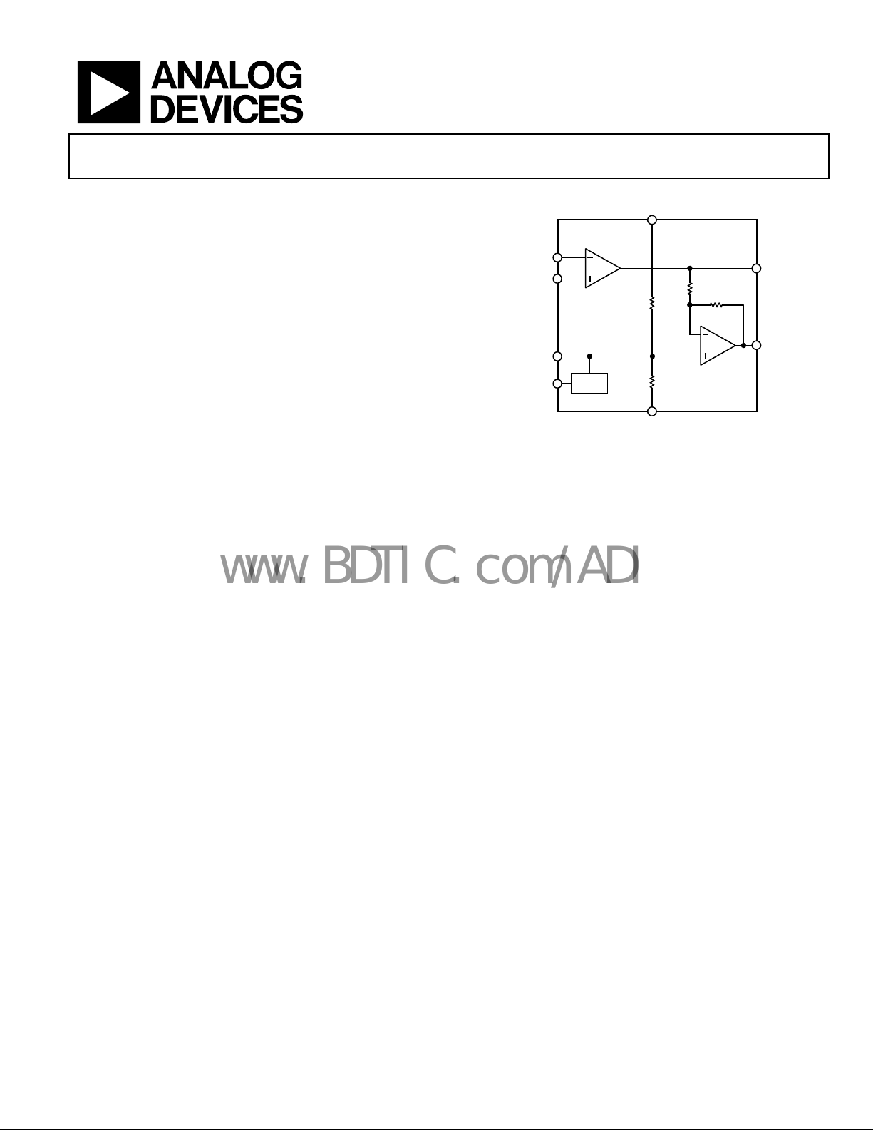
FUNCTIONAL BLOCK DIAGRAM
IN–
IN+
BYPASS
SHUTDOWN
The low differential dc output voltage results in negligible
losses in the speaker winding and makes high value dc blocking
capacitors unnecessary. The battery life is extended by using
shutdown mode, which typically reduces quiescent current
drain to 100 nA.
The SSM2211 is designed to operate over the −40°C to +85°C
temperature range. The SSM2211 is available in 8-lead SOIC
(narrow body) and LFCSP (lead frame chip scale) surfacemount packages. The advanced mechanical packaging of the
LFCSP models ensures lower chip temperature and enhanced
performance relative to standard packaging options.
Applications include personal portable computers, hands-free
telephones and transceivers, talking toys, intercom systems, and
other low voltage audio systems requiring 1 W output power.
One Technology Way, P.O. Box 9106, Norwood, MA 02062-9106, U.S.A.
Tel: 781.329.4700 www.analog.com
Fax: 781.461.3113 ©2008 Analog Devices, Inc. All rights reserved.
BIAS
SSM2211
V– (GND)
Figure 1.
A
V
OUT
V
B
OUT
00358-001
Page 2

SSM2211
www.BDTIC.com/ADI
TABLE OF CONTENTS
Features .............................................................................................. 1
Applications ....................................................................................... 1
Functional Block Diagram .............................................................. 1
General Description ......................................................................... 1
Revision History ............................................................................... 2
Electrical Characteristics ................................................................. 3
Absolute Maximum Ratings ............................................................ 5
Thermal Resistance ...................................................................... 5
ESD Caution .................................................................................. 5
Pin Configurations and Function Descriptions ........................... 6
Typical Performance Characteristics ............................................. 7
Product Overview ........................................................................... 14
Thermal Performance—LFCSP ................................................ 14
Typical Applications ....................................................................... 15
Bridged Output vs. Single-Ended Output Configurations ... 15
Speaker Efficiency and Loudness ............................................. 15
Power Dissipation....................................................................... 16
Output Voltage Headroom ........................................................ 17
Automatic Shutdown-Sensing Circuit ..................................... 17
Shutdown-Circuit Design Example ......................................... 18
Start-Up Popping Noise ............................................................. 18
SSM2211 Amplifier Design Example .................................. 18
Single-Ended Applications ........................................................ 19
Driving Two Speakers Single Endedly ..................................... 19
Evaluation Board ........................................................................ 20
LFCSP PCB Considerations ...................................................... 20
Outline Dimensions ....................................................................... 21
Ordering Guide .......................................................................... 22
REVISION HISTORY
4/08—Rev. D to Rev. E
Changes to Features .......................................................................... 1
Changes to General Description .................................................... 1
Changes to Supply Current in Table 1 and Table 2 ...................... 3
Changes to Supply Current in Table 3 ........................................... 4
Changes to Absolute Maximum Ratings ....................................... 5
Changes to Figure 41 ...................................................................... 14
Changes to Equation 7, Equation 8, and Equation 10 ............... 16
Changes to Figure 47 ...................................................................... 17
Changes to Automatic Shutdown-Sensing Circuit Section ...... 18
Changes to SSM2211Amplifier Design Example Section ......... 19
Changes to Driving Two Speakers Single Endedly Section ...... 20
Changes to Figure 50 ...................................................................... 20
Changes to Evaluation Board Section .......................................... 20
Changes to Figure 51 ...................................................................... 20
Changes to Ordering Guide .......................................................... 22
11/06—Rev. C to Rev. D
Updated Format .................................................................. Universal
Changes to General Description .................................................... 1
Changes to Electrical Characteristics ............................................ 3
Changes to Absolute Maximum Ratings ....................................... 5
Added Table 6 .................................................................................... 6
Changes to Figure 32 ...................................................................... 11
Changes to the Product Overview Section ................................. 14
Changes to the Output Voltage Headroom Section ................... 17
Changes to the Start-Up Popping Noise Section ........................ 18
Changes to the Evaluation Board Section ................................... 20
Updated Outline Dimensions ....................................................... 21
Changes to Ordering Guide .......................................................... 21
10/04—Data Sheet Changed from Rev. B to Rev. C
Updated Format .................................................................. Universal
Changes to General Description ..................................................... 1
Changes to Table 5 ............................................................................. 4
Deleted Thermal Performance—SOIC Section ........................... 8
Changes to Figure 31 ...................................................................... 10
Changes to Figure 40 ...................................................................... 12
Changes to Thermal Performance—LFCSP Section ................. 13
Deleted Figure 52, Renumbered Successive Figures .................. 14
Deleted Printed Circuit Board Layout—SOIC Section ............. 14
Changes to Output Voltage Headroom Section ......................... 16
Changes to Start-Up Popping Noise Section .............................. 17
Changes to Ordering Guide .......................................................... 20
10/02—Data Sheet Changed from Rev. A to Rev. B
Deleted 8-Lead PDIP ......................................................... Universal
Updated Outline Dimensions ....................................................... 15
5/02—Data Sheet Changed from Rev. 0 to Rev. A
Edits to General Description ........................................................... 1
Edits to Package Type ....................................................................... 3
Edits to Ordering Guide ................................................................... 3
Edits to Product Overview ............................................................... 8
Edits to Printed Circuit Board Layout Considerations ............. 13
Added section Printed Circuit Board Layout
Considerations—LFCSP ................................................................ 14
Rev. E | Page 2 of 24
Page 3

SSM2211
www.BDTIC.com/ADI
ELECTRICAL CHARACTERISTICS
VDD = 5.0 V, TA = 25°C, RL = 8 Ω, CB = 0.1 µF, VCM = VDD/2, unless otherwise noted.
Table 1.
Parameter Symbol Conditions Min Typ Max Unit
GENERAL CHARACTERISTICS
Differential Output Offset Voltage V
Output Impedance Z
SHUTDOWN CONTROL
Input Voltage High VIH ISY = <100 mA 3.0 V
Input Voltage Low VIL ISY = normal 1.3 V
POWER SUPPLY
Power Supply Rejection Ratio PSRR VS = 4.75 V to 5.25 V 66 dB
Supply Current ISY V
Supply Current, Shutdown Mode ISD Pin 1 = VDD (see Figure 32), −40°C ≤ TA ≤ +85°C 0.1 1 μA
DYNAMIC PERFORMANCE
Gain Bandwidth Product GBP 4 MHz
Phase Margin ΦM 86 Degrees
AUDIO PERFORMANCE
Total Harmonic Distortion THD + N P = 0.5 W into 8 Ω, f = 1 kHz 0.15 %
Total Harmonic Distortion THD + N P = 1.0 W into 8 Ω, f = 1 kHz 0.2 %
Voltage Noise Density en f = 1 kHz 85
AVD = 2, −40°C ≤ TA ≤ +85°C 4 50 mV
OOS
0.1 Ω
OUT
A = V
OUT
B = 2.5 V, −40°C ≤ TA ≤ +85°C 9.5 20 mA
OUT
nV√Hz
VDD = 3.3 V, TA = 25°C, RL = 8 Ω, CB = 0.1 µF, VCM = VDD/2, unless otherwise noted.
Table 2.
Parameter Symbol Conditions Min Typ Max Unit
GENERAL CHARACTERISTICS
Differential Output Offset Voltage V
Output Impedance Z
SHUTDOWN CONTROL
Input Voltage High VIH ISY = <100 μA 1.7 V
Input Voltage Low VIL ISY = normal 1 V
POWER SUPPLY
Supply Current ISY V
Supply Current, Shutdown Mode ISD Pin 1 = VDD (see Figure 32), −40°C ≤ TA ≤ +85°C 0.1 1 μA
AUDIO PERFORMANCE
Total Harmonic Distortion THD + N P = 0.35 W into 8 Ω, f = 1 kHz 0.1 %
AVD = 2, −40°C ≤ TA ≤ +85°C 5 50 mV
OOS
0.1 Ω
OUT
A = V
OUT
B = 1.65 V, −40°C ≤ TA ≤ +85°C 5.2 20 mA
OUT
Rev. E | Page 3 of 24
Page 4
SSM2211
www.BDTIC.com/ADI
VDD = 2.7 V, TA = 25°C, RL = 8 Ω, CB = 0.1 µF, VCM = VDD/2, unless otherwise noted.
Table 3.
Parameter Symbol Conditions Min Typ Max Unit
GENERAL CHARACTERISTICS
Differential Output Offset Voltage V
Output Impedance Z
SHUTDOWN CONTROL
Input Voltage High VIH ISY = <100 mA 1.5 V
Input Voltage Low VIL ISY = normal 0.8 V
POWER SUPPLY
Supply Current ISY V
Supply Current, Shutdown Mode ISD Pin 1 = VDD (see Figure 32), −40°C ≤ TA ≤ +85°C 0.1 1 μA
AUDIO PERFORMANCE
Total Harmonic Distortion THD + N P = 0.25 W into 8 Ω, f = 1 kHz 0.1 %
AVD = 2 5 50 mV
OOS
0.1 Ω
OUT
A = V
OUT
B = 1.35 V, −40°C ≤ TA ≤ +85°C 4.2 20 mA
OUT
Rev. E | Page 4 of 24
Page 5
SSM2211
www.BDTIC.com/ADI
ABSOLUTE MAXIMUM RATINGS
Absolute maximum ratings apply at TA = 25°C, unless
otherwise noted.
Table 4.
Parameter Rating
Supply Voltage 6 V
Input Voltage VDD
Common-Mode Input Voltage VDD
ESD Susceptibility 2000 V
Storage Temperature Range −65°C to +150°C
Operating Temperature Range −40°C to +85°C
Junction Temperature Range −65°C to +165°C
Lead Temperature, Soldering (60 sec) 300°C
Stresses above those listed under Absolute Maximum Ratings
may cause permanent damage to the device. This is a stress
rating only; functional operation of the device at these or any
other conditions above those indicated in the operational
section of this specification is not implied. Exposure to absolute
maximum rating conditions for extended periods may affect
device reliability.
THERMAL RESISTANCE
is specified for the worst-case conditions, that is, a device
θ
JA
soldered in a circuit board for surface-mount packages.
Table 5. Thermal Resistance
Package Type θJA Unit
8-Lead LFCSP_VD (CP-Suffix)1 50 °C/W
8-Lead SOIC_N (S-Suffix)2 121 °C/W
1
For the LFCSP_VD, θJA is measured with exposed lead frame soldered to the PCB.
2
For the SOIC_N, θJA is measured with the device soldered to a four-layer PCB.
ESD CAUTION
Rev. E | Page 5 of 24
Page 6
SSM2211
www.BDTIC.com/ADI
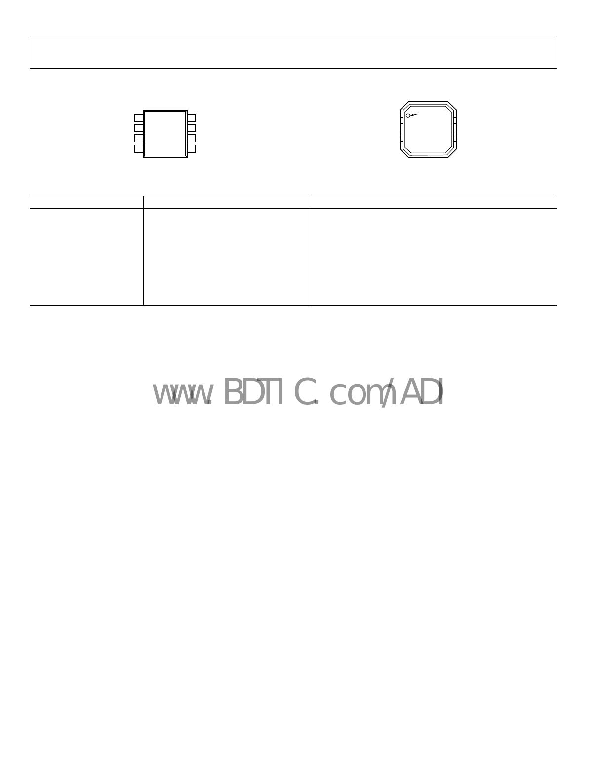
PIN CONFIGURATIONS AND FUNCTION DESCRIPTIONS
PIN 1
1SHUTDOWN
SHUTDOWN
BYPASS
IN+
IN–
1
SSM2211
2
3
TOP VIEW
(Not to Scale)
4
V
B
8
OUT
V–
7
6
V+
V
A
5
OUT
00358-002
2BYPASS
3IN+
4IN–
INDICATO R
SSM2211
TOP VIEW
(Not to Scale)
Figure 2. 8-Lead SOIC_N Pin Configuration (R-8) Figure 3. 8-Lead LFCSP_VD Pin Configuration (CP-8-2)
Table 6. Pin Function Descriptions
Pin No. Mnemonic Description
1 SHUTDOWN Shutdown Enable.
2 BYPASS Bypass Capacitor.
3 IN+ Noninverting Input.
4 IN− Inverting Input.
5 V
A Output A.
OUT
6 V+ Positive Supply.
7 V− Negative Supply.
8 V
B Output B.
OUT
8V
7V–
6V+
5V
OUT
OUT
B
A
00358-003
Rev. E | Page 6 of 24
Page 7
SSM2211
www.BDTIC.com/ADI
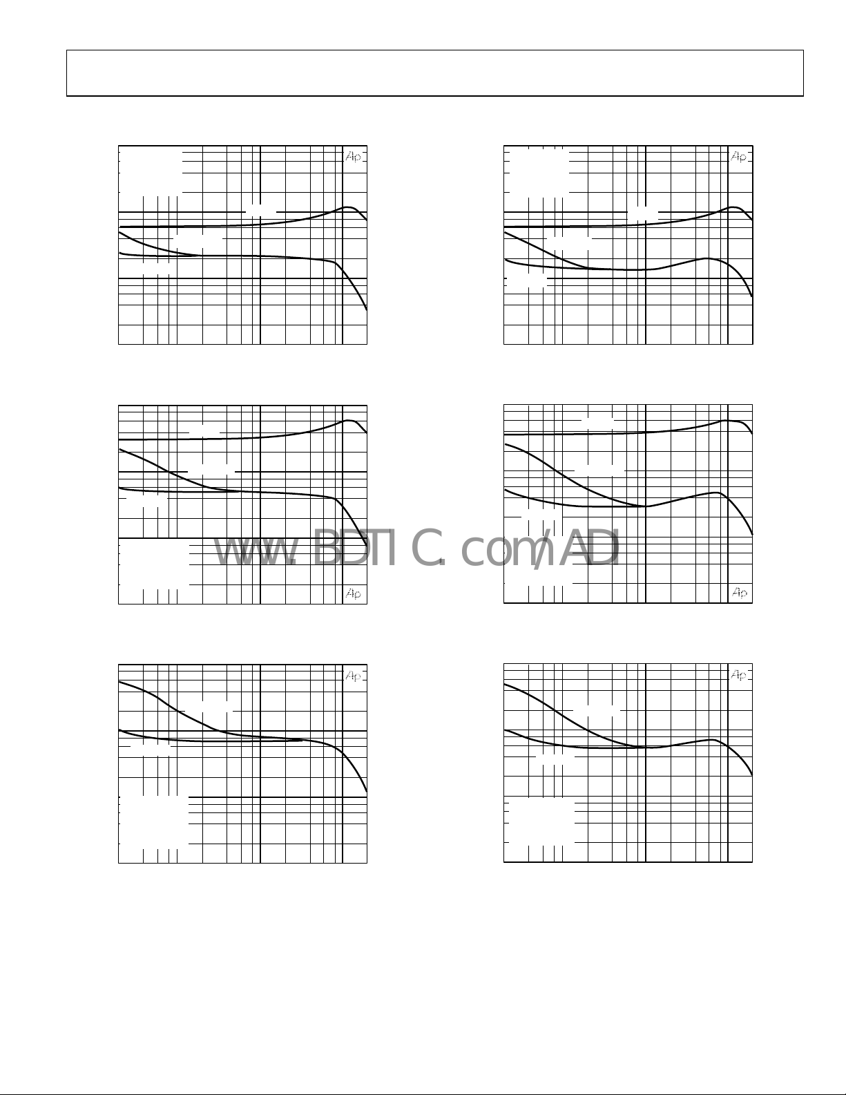
TYPICAL PERFORMANCE CHARACTERISTICS
10
1
TA = 25°C
V
= 5V
DD
A
= 2 (BTL)
VD
R
= 8Ω
L
P
= 500mW
L
CB = 0
10
1
TA = 25°C
V
= 5V
DD
A
= 2 (BTL)
VD
R
= 8Ω
L
P
= 1W
L
CB = 0
CB = 0.1μF
THD + N (%)
CB = 1μF
0.1
0.01
20 100 20k
FREQUENCY (Hz)
1k 10k
Figure 4. THD + N vs. Frequency
10
CB = 0
1
CB = 1μF
THD + N (%)
0.1
TA = 25°C
V
= 5V
DD
A
= 10 (BTL)
VD
R
= 8Ω
L
P
= 500mW
L
0.01
20 100 20k
CB = 0.1μF
1k 10k
FREQUENCY (Hz)
Figure 5. THD + N vs. Frequency
10
00358-004
00358-005
CB = 0.1μF
THD + N (%)
0.1
CB = 1μF
0.01
20 100 20k
FREQUENCY (Hz)
1k 10k
Figure 7. THD + N vs. Frequency
10
CB = 0
1
THD + N (%)
CB = 1μF
0.1
TA = 25°C
V
= 5V
DD
A
= 10 (BTL)
VD
R
= 8Ω
L
P
= 1W
L
0.01
20 100 20k
CB = 0.1μF
1k 10k
FREQUENCY (Hz)
Figure 8. THD + N vs. Frequency
10
00358-007
00358-008
CB = 0.1μF
1
CB = 1μF
THD + N (%)
0.1
TA = 25°C
V
= 5V
DD
A
= 20 (BTL)
VD
R
= 8Ω
L
P
= 500mW
L
0.01
20 100 20k
FREQUENCY (Hz)
1k 10k
00358-006
Figure 6. THD + N vs. Frequency
Rev. E | Page 7 of 24
CB = 0.1μF
1
CB = 1μF
THD + N (%)
0.1
TA = 25°C
V
= 5V
DD
A
= 20 (BTL)
VD
R
= 8Ω
L
P
= 1W
L
0.01
20 100 20k
FREQUENCY (Hz)
1k 10k
Figure 9. THD + N vs. Frequency
00358-009
Page 8
SSM2211
www.BDTIC.com/ADI
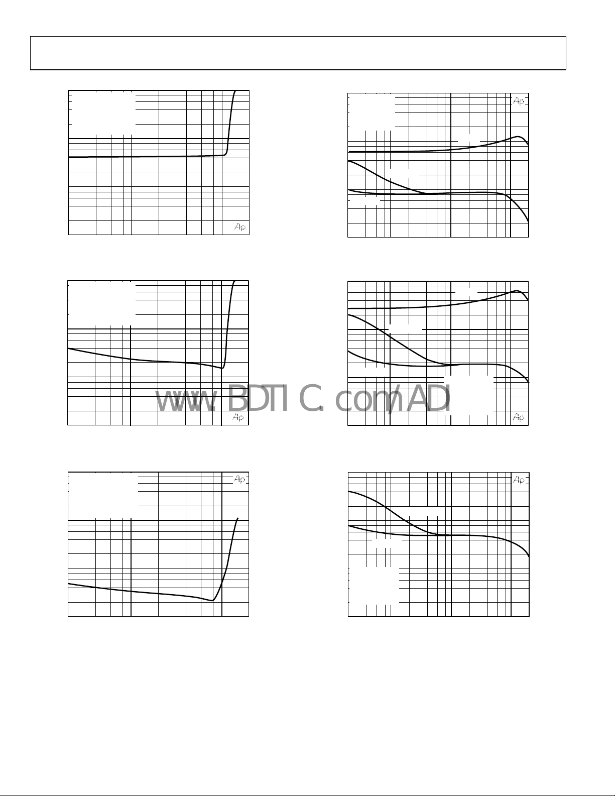
10
TA = 25°C
V
= 5V
DD
A
= 2 (BTL)
VD
R
= 8Ω
L
FREQUENCY = 20Hz
C
= 0.1μF
B
1
10
1
TA = 25°C
V
= 3.3V
DD
A
= 2 (BTL)
VD
R
= 8Ω
L
P
= 350mW
L
CB = 0
THD + N (%)
0.1
0.01
20n 0.1 2
10
TA = 25°C
= 5V
V
DD
= 2 (BTL)
A
VD
= 8Ω
R
L
FREQUENCY = 1kHz
C
= 0.1μF
B
1
THD + N (%)
0.1
0.01
20n 0.1 2
10
TA = 25°C
V
= 5V
DD
A
= 2 (BTL)
VD
R
= 8Ω
L
FREQUENCY = 20kHz
C
= 0.1μF
B
1
P
(W)
OUTPUT
Figure 10. THD + N vs. P
P
(W)
OUTPUT
Figure 11. THD + N vs. P
OUTPUT
OUTPUT
THD + N (%)
0.1
CB = 1μF
1
00358-010
0.01
20 100 20k
CB = 0.1μF
FREQUENCY (Hz)
1k 10k
00358-013
Figure 13. THD + N vs. Frequency
10
CB = 0
1
THD + N (%)
1
00358-011
CB = 1μF
0.1
0.01
20 100 20k
CB = 0.1μF
TA = 25°C
V
DD
A
VD
R
= 8Ω
L
P
= 350mW
L
FREQUENCY (Hz)
1k 10k
= 3.3V
= 10 (BTL)
00358-014
Figure 14. THD + N vs. Frequency
10
1
CB = 0.1μF
THD + N (%)
0.1
0.01
20n 0.1 2
P
(W)
OUTPUT
Figure 12. THD + N vs. P
OUTPUT
1
00358-012
Rev. E | Page 8 of 24
CB = 1μF
THD + N (%)
0.1
TA = 25°C
V
= 3.3V
DD
A
= 20 (BTL)
VD
R
= 8Ω
L
P
= 350mW
L
0.01
20 100 20k
FREQUENCY (Hz)
1k 10k
Figure 15. THD + N vs. Frequency
00358-015
Page 9

SSM2211
www.BDTIC.com/ADI
10
1
THD + N (%)
0.1
TA = 25°C
V
= 3.3V
DD
A
= 2 (BTL)
VD
R
= 8Ω
L
FREQUENCY = 20Hz
C
= 0.1μF
B
10
1
THD + N (%)
0.1
TA = 25°C
= 2.7V
V
DD
A
= 2 (BTL)
VD
= 8Ω
R
L
= 250mW
P
L
CB = 1μF
CB = 0
CB = 0.1μF
0.01
20n 0.1 2
10
TA = 25°C
= 3.3V
V
DD
= 2 (BTL)
A
VD
= 8Ω
R
L
FREQUENCY = 1kHz
C
= 0.1μF
B
1
THD + N (%)
0.1
0.01
20n 0.1 2
10
TA = 25°C
V
= 3.3V
DD
= 2 (BTL)
A
VD
R
= 8Ω
L
FREQUENCY = 20kHz
C
= 0.1μF
B
1
P
(W)
OUTPUT
Figure 16. THD + N vs. P
P
(W)
OUTPUT
Figure 17. THD + N vs. P
OUTPUT
OUTPUT
1
00358-016
0.01
20 100 20k
FREQUENCY (Hz)
1k 10k
00358-019
Figure 19. THD + N vs. Frequency
10
CB = 0
1
THD + N (%)
0.1
1
00358-017
0.01
20 100 20k
CB = 0.1μF
CB = 1μF
FREQUENCY (Hz)
1k 10k
TA = 25°C
= 2.7V
V
DD
A
= 10 (BTL)
VD
= 8Ω
R
L
= 250mW
P
L
00358-020
Figure 20. THD + N vs. Frequency
10
CB = 0.1μF
1
THD + N (%)
0.1
0.01
20n 0.1 2
P
(W)
OUTPUT
Figure 18. THD + N vs. P
OUTPUT
1
00358-018
Rev. E | Page 9 of 24
THD + N (%)
0.1
0.01
CB = 1μF
TA = 25°C
= 2.7V
V
DD
= 20 (BTL)
A
VD
= 8Ω
R
L
P
= 250mW
L
20 100 20k
FREQUENCY (Hz)
1k 10k
Figure 21. THD + N vs. Frequency
00358-021
Page 10

SSM2211
www.BDTIC.com/ADI
10
TA = 25°C
V
= 2.7V
DD
A
= 2 (BTL)
VD
R
= 8Ω
L
FREQUENCY = 20Hz
1
THD + N (%)
0.1
0.01
20n 0.1 2
P
(W)
OUTPUT
Figure 22. THD + N vs. P
OUTPUT
1
00358-022
10
TA = 25°C
V
= 5V
DD
A
= 10 SINGLE ENDED
VD
C
= 0.1μF
B
C
= 1000μF
C
1
RL = 8Ω
P
= 250mW
THD + N (%)
0.1
RL = 32Ω
P
= 60mW
O
0.01
20 100 20k
O
1k 10k
FREQUENCY (Hz)
Figure 25. THD + N vs. Frequency
00358-025
10
TA = 25°C
V
= 2.7V
DD
A
= 2 (BTL)
VD
R
= 8Ω
L
FREQUENCY = 1kHz
1
THD + N (%)
0.1
0.01
20n 0.1 2
10
TA = 25°C
V
= 2.7V
DD
A
= 2 (BTL)
VD
R
= 8Ω
L
FREQUENCY = 20kHz
1
THD + N (%)
0.1
P
(W)
OUTPUT
Figure 23. THD + N vs. P
OUTPUT
10
TA = 25°C
V
= 3.3V
DD
A
= 10 SINGLE ENDED
VD
C
= 0.1μF
B
C
= 1000μF
C
1
RL = 8Ω
P
= 85mW
THD + N (%)
0.1
RL = 32Ω
P
= 20mW
O
1
00358-023
0.01
20 100 20k
Figure 26. THD + N vs. Frequency
10
TA = 25°C
V
= 2.7V
DD
A
= 10 SINGLE ENDED
VD
C
= 0.1μF
B
C
= 1000μF
C
1
THD + N (%)
0.1
O
= 65mW
O
1k 10k
FREQUENCY (Hz)
RL = 8Ω
P
00358-026
0.01
20n 0.1 2
P
(W)
OUTPUT
Figure 24. THD + N vs. P
OUTPUT
1
00358-024
Rev. E | Page 10 of 24
RL = 32Ω
P
= 15mW
O
0.01
20 100 20k
FREQUENCY (Hz)
1k 10k
Figure 27. THD + N vs. Frequency
00358-027
Page 11

SSM2211
A
www.BDTIC.com/ADI
10
TA = 25°C
A
= 2 (BTL)
VD
R
= 8Ω
L
FREQUENCY = 20Hz
C
= 0.1μF
B
1
VDD = 2.7V
4.0
3.5
3.0
2.5
T
= 150°C
J,MAX
FREE AIR, NO HEAT SINK
= 121°C/W
SOIC θ
JA
LFCSP θ
8-LEAD LFCSP
= 50°C/W
JA
THD + N (%)
0.1
0.01
20n 0.1 2
Figure 28. THD + N vs. P
10
TA = 25°C
A
= 2 (BTL)
VD
R
= 8Ω
L
FREQUENCY = 1kHz
C
= 0.1μF
B
1
THD + N (%)
0.1
0.01
20n 0.1 2
Figure 29. THD + N vs. P
10
TA = 25°C
A
= 2 (BTL)
VD
R
= 8Ω
L
FREQUENCY = 20kHz
C
= 0.1μF
B
1
VDD = 3.3V
P
OUTPUT
VDD = 2.7V
P
OUTPUT
VDD = 2.7V
(W)
VDD = 3.3V
(W)
VDD = 3.3V
OUTPUT
OUTPUT
VDD = 5V
1
VDD = 5V
1
00358-028
00358-029
2.0
1.5
1.0
8-LEAD SOIC
MAXIMUM POWER DISSIPATION (W)
0.5
0
–40 –30 –20 –10 0 10 30 7020 40 50 60 9080 110100 120
AMBIENT TEMPERATURE (°C)
00358-031
Figure 31. Maximum Power Dissipation vs. Ambient Temperature
10k
8k
)
6k
4k
SUPPLY CURRENT (µ
2k
0
05
1234
SHUTDOWN VO LTAGE AT PIN 1 (V)
TA = 25°C
V
= 5V
DD
00358-032
Figure 32. Supply Current vs. Shutdown Voltage at Pin 1
14
TA = 25°C
12
R
= OPEN
L
10
8
THD + N (%)
0.1
OUTPUT
VDD = 5V
0.01
20n 0.1 2
P
OUTPUT
(W)
Figure 30. THD + N vs. P
1
00358-030
Rev. E | Page 11 of 24
6
4
SUPPLY CURRENT (mA)
2
0
01 6
2345
SUPPLY VOLTAGE (V)
Figure 33. Supply Current vs. Supply Voltage
00358-033
Page 12

SSM2211
www.BDTIC.com/ADI
1.6
1.4
1.2
25
VDD = 2.7V
SAMPLE SIZE = 300
20
1.0
0.8
0.6
OUTPUT POWER (W)
0.4
0.2
0
48 4812 16 20 24 28 32 36 40 44
Figure 34. P
80
60
40
20
0
GAIN (dB)
–20
–40
–60
–80
100 1k 100M
2.7V
LOAD RESISTANCE (Ω)
vs. Load Resistance
OUTPUT
10k 100k 1M 10M
FREQUENCY (Hz)
3.3V
Figure 35. Gain and Phase Shift vs. Frequency (Single Amplifier)
15
10
NUMBER OF UNITS
5V
00358-034
5
0
–20 –15 25–10 –5 0 10 15 205
OUTPUT OFFSET VOLTAGE (mV)
00358-036
Figure 36. Output Offset Voltage Distribution
180
135
90
45
0
–45
–90
–135
–180
PHASE SHIFT (Degrees)
00358-035
20
VDD = 3.3V
SAMPLE SIZE = 300
16
12
8
NUMBER OF UNIT S
4
0
–30 –20 30–10 0 10 20
OUTPUT OFF SET VOLTAGE (mV)
00358-037
Figure 37. Output Offset Voltage Distribution
Rev. E | Page 12 of 24
Page 13

SSM2211
www.BDTIC.com/ADI
20
16
12
VDD = 3.3V
VDD = 5V
SAMPLE SIZE = 300
SAMPLE SIZE = 300
–50
–55
TA = 25°C
V
= 5V± 100mV
DD
C
= 15μF
B
A
= 2
VD
8
NUMBER OF UNIT S
4
0
–30 –20 30
–10 0 10 20
OUTPUT OFFSET VOLTAGE (mV)
Figure 38. Output Offset Voltage Distribution
600
500
400
300
NUMBER OF UNITS
200
100
0
6 7 8 9 10 11 12 13 14 15
SUPPLY CURRENT (mA)
VDD = 5V
SAMPLE SIZE = 1,700
Figure 39. Supply Current Distribution
–60
PSRR (dB)
–65
00358-038
–70
20 100 30k1k 10k
FREQUENCY (Hz)
00358-040
Figure 40. PSRR vs. Frequency
00358-039
Rev. E | Page 13 of 24
Page 14

SSM2211
Ω
www.BDTIC.com/ADI
PRODUCT OVERVIEW
The SSM2211 is a low distortion speaker amplifier that can run
from a 2.7 V to 5.5 V supply. It consists of a rail-to-rail input
and a differential output that can be driven within 400 mV of
either supply rail while supplying a sustained output current of
350 mA. The SSM2211 is unity-gain stable, requiring no
external compensation capacitors, and can be configured for
gains of up to 40 dB. Figure 41 shows the simplified schematic.
20k
V+
6
IN–
20kΩ
4
A1
3
50kΩ
2
SSM2211
50kΩ
50kΩ
A2
5
8
A
V
OUT
V
B
OUT
Pin 4 and Pin 3 are the inverting and noninverting terminals
to A1. An offset voltage is provided at Pin 2, which should be
connected to Pin 3 for use in single-supply applications. The
output of A1 appears at Pin 5. A second operational amplifier,
A2, is configured with a fixed gain of A
= −1 and produces an
V
inverted replica of Pin 5 at Pin 8. The SSM2211 outputs at Pin 5
and Pin 8 produce a bridged configuration output to which a
speaker can be connected. This bridge configuration offers the
advantage of a more efficient power transfer from the input to
the speaker. Because both outputs are symmetric, the dc bias at
Pin 5 and Pin 8 are exactly equal, resulting in zero dc differential
voltage across the outputs. This eliminates the need for a coupling
capacitor at the output.
THERMAL PERFORMANCE—LFCSP
The LFCSP offers the SSM2211 user even greater choices when
considering thermal performance criteria. For the 8-lead,
3 mm × 3 mm LFCSP, the θ
performance improvement over most other packaging options.
is 50°C/W. This is a significant
JA
0.1µF
50kΩ
7
Figure 41. Simplified Schematic
BIAS
CONTROL
1
SHUTDOWN
00358-041
Rev. E | Page 14 of 24
Page 15

SSM2211
A
www.BDTIC.com/ADI
TYPICAL APPLICATIONS
R
F
5V
C
S
5
8
1
7
–
+
SPEAKER
8V
00358-042
UDIO
INPUT
C
C
R
I
Figure 42. Typical Configuration
4
–
SSM2211
3
+
2
C
B
6
Figure 42 shows how the SSM2211 is connected in a typical
application. The SSM2211 can be configured for gain much like
a standard operational amplifier. The gain from the audio input
to the speaker is
R
F
A ×= 2
V
(1)
R
I
The 2× factor results from Pin 8 having an opposite polarity of
Pin 5, providing twice the voltage swing to the speaker from the
bridged-output (BTL) configuration.
C
is a supply bypass capacitor used to provide power supply
S
filtering. Pin 2 is connected to Pin 3 to provide an offset voltage
for single-supply use, with C
providing a low ac impedance to
B
ground to enhance power-supply rejection. Because Pin 4 is a
virtual ac ground, the input impedance is equal to R
. CC is the
I
input coupling capacitor, which also creates a high-pass filter
with a corner frequency of
1
HP
(2)
CRf×π=2
I
C
Because the SSM2211 has an excellent phase margin, a feedback
capacitor in parallel with R
to band limit the amplifier is not
F
required, as it is in some competitor products.
BRIDGED OUTPUT VS. SINGLE-ENDED OUTPUT CONFIGURATIONS
The power delivered to a load with a sinusoidal signal can be
expressed in terms of the peak voltage of the signal and the
resistance of the load as
2
V
PK
P×=
L
2
By driving a load from a BTL configuration, the voltage swing
across the load doubles. Therefore, an advantage in using a BTL
configuration becomes apparent from Equation 3, as doubling
the peak voltage results in four times the power delivered to the
load. In a typical application operating from a 5 V supply, the
maximum power that can be delivered by the SSM2211 to an
8 Ω speaker in a single-ended configuration is 250 mW. By
(3)
R
L
driving this speaker with a bridged output, 1 W of power can be
delivered. This translates to a 12 dB increase in sound pressure
level from the speaker.
Driving a speaker differentially from a BTL offers another
advantage in that it eliminates the need for an output coupling
capacitor to the load. In a single-supply application, the quiescent
voltage at the output is half of the supply voltage. If a speaker is
connected in a single-ended configuration, a coupling capacitor
is needed to prevent dc current from flowing through the speaker.
This capacitor also needs to be large enough to prevent low
frequency roll-off. The corner frequency is given by
1
(4)
CRf×
C
where R
=
−
dB3
π2
L
is the speaker resistance and CC is the coupling
L
capacitance.
For an 8 Ω speaker and a corner frequency of 20 Hz, a 1000 µF
capacitor is needed, which is physically large and costly. By
connecting a speaker in a BTL configuration, the quiescent
differential voltage across the speaker becomes nearly zero,
eliminating the need for the coupling capacitor.
SPEAKER EFFICIENCY AND LOUDNESS
The effective loudness of 1 W of power delivered into an 8 Ω
speaker is a function of speaker efficiency. The efficiency is
typically rated as the sound pressure level (SPL) at 1 meter in
front of the speaker with 1 W of power applied to the speaker.
Most speakers are between 85 dB and 95 dB SPL at 1 meter at
1 W. Ta ble 7 shows a comparison of the relative loudness of
different sounds.
Table 7. Typical Sound Pressure Levels
Source of Sound SPL (dB)
Threshold of Pain 120
Heavy Street Traffic 95
Cabin of Jet Aircraft 80
Average Conversation 65
Average Home at Night 50
Quiet Recording Studio 30
Threshold of Hearing 0
Consequently, Tabl e 7 demonstrates that 1 W of power into a
speaker can produce quite a bit of acoustic energy.
Rev. E | Page 15 of 24
Page 16

SSM2211
www.BDTIC.com/ADI
POWER DISSIPATION
Another important advantage in using a BTL configuration is
the fact that bridged-output amplifiers are more efficient than
single-ended amplifiers in delivering power to a load. Efficiency
is defined as the ratio of the power from the power supply to the
power delivered to the load
P
L
=η
P
SY
An amplifier with a higher efficiency has less internal power
dissipation, which results in a lower die-to-case junction
temperature compared with an amplifier that is less efficient.
This is important when considering the amplifier maximum
power dissipation rating vs. ambient temperature. An internal
power dissipation vs. output power equation can be derived to
fully understand this.
The internal power dissipation of the amplifier is the internal
voltage drop multiplied by the average value of the supply
current. An easier way to find internal power dissipation is to
measure the difference between the power delivered by the
supply voltage source and the power delivered into the load.
The waveform of the supply current for a bridged-output
amplifier is shown in Figure 43.
V
OUT
V
PEAK
TIME
T
I
SY
The power dissipated internally by the amplifier is simply the
difference between Equation 6 and Equation 3. The equation
for internal power dissipated, P
, expressed in terms of power
DISS
delivered to the load and load resistance, is
V
22
P −×
=
DISS
DD
R
π
L
PP
(7)
LL
The graph of this equation is shown in Figure 44.
1.5
VDD = 5V
RL = 4Ω
1.0
0.5
POWER DISSIPATION (W)
RL = 16Ω
0
0 1.5
Figure 44. Power Dissipation vs. Output Power with V
0.5 1.0
OUTPUT POWER (W)
RL = 8Ω
DD
00358-044
= 5 V
Because the efficiency of a bridged-output amplifier (Equation 3
divided by Equation 6) increases with the square root of P
, the
L
power dissipated internally by the device stays relatively flat and
actually decreases with higher output power. The maximum
power dissipation of the device can be found by differentiating
Equation 7 with respect to load power and setting the derivative
equal to zero. This yields
I
DD, PEAK
I
DD, AVG
T
Figure 43. Bridged Amplifier Output Voltage and Supply Current vs. Time
TIME
00358-043
By integrating the supply current over a period, T, and then
dividing the result by T, the I
can be found. Expressed in
DD,AVG
terms of peak output voltage and load resistance
V
2
PEAK
I
= (5)
AVGDD
,
R
π
L
Therefore, power delivered by the supply, neglecting the bias
current for the device, is
VV
×
2
DD
PEAK
P
=
SY
R
π
(6)
L
and occurs when
Using Equation 9 and the power derating curve in Figure 31,
the maximum ambient temperature can be found easily. This
ensures that the SSM2211 does not exceed its maximum
junction temperature of 150°C. The power dissipation for a
single-ended output application where the load is capacitively
coupled is given by
The graph of Equation 10 is shown in Figure 45.
Rev. E | Page 16 of 24
2
∂
P
DISS
∂
P
L
P
,
MAXDISS
P −×
DISS
V
DD
=
π
V
2
DD
=
2
R
π
22
V
=
DD
R
π
L
1
PR
LL
2
01
=−×
(8)
(9)
L
PP
(10)
LL
Page 17

SSM2211
www.BDTIC.com/ADI
0.35
0.30
0.25
0.20
0.15
0.10
POWER DISSIPATION (W)
0.05
0
VDD = 5V
0 0.40.1
RL = 16Ω
0.2 0.3
OUTPUT POWER (W)
RL = 4Ω
RL = 8Ω
00358-045
Figure 45. Power Dissipation vs. Single-Ended Output Power
= 5 V
with V
DD
The maximum power dissipation for a single-ended output is
2
V
P
MAXDISS
,
DD
= (11)
2
R
π2
L
OUTPUT VOLTAGE HEADROOM
The outputs of both amplifiers in the SSM2211 can come within
400 mV of either supply rail while driving an 8 Ω load. As
compared with equivalent competitor products, the SSM2211
has a higher output voltage headroom. This means that the
SSM2211 can deliver an equivalent maximum output power
while running from a lower supply voltage. By running at a lower
supply voltage, the internal power dissipation of the device is
reduced, as shown in Equation 9. This extended output
headroom, along with the LFCSP, allows the SSM2211 to
operate in higher ambient temperatures than competitor
devices.
The SSM2211 is also capable of providing amplification even at
supply voltages as low as 2.7 V. The maximum power available at
the output is a function of the supply voltage. Therefore, as the
supply voltage decreases, so does the maximum power output
from the device. The maximum output power vs. supply voltage
at various BTL resistances is shown in Figure 46. The maximum
output power is defined as the point at which the output has 1%
total harmonic distortion (THD + N).
To find the minimum supply voltage needed to achieve a
specified maximum undistorted output power use Figure 46.
For example, an application requires only 500 mW to be output
for an 8 Ω speaker. With the speaker connected in a bridgedoutput configuration, the minimum supply voltage required
is 3.3 V.
1.6
1.4
@ 1% THD (W)
OUT
MAX P
1.2
1.0
0.8
0.6
0.4
0.2
0
1.5 5.02.0
2.5 3.0 3.5 4.0 4. 5
SUPPLY VOLTAGE (V)
RL = 4Ω
= 8Ω
R
L
RL = 16Ω
00358-046
Figure 46. Maximum Output Power vs. VSY
Shutdown Feature
The SSM2211 can be put into a low power consumption shutdown mode by connecting Pin 1 to 5 V. In shutdown mode,
the SSM2211 has an extremely low supply current of less than
10 nA. This makes the SSM2211 ideal for battery-powered
applications.
Connect Pin 1 to ground for normal operation. Connecting Pin 1
to V
mutes the outputs and puts the device into shutdown
DD
mode. A pull-up or pull-down resistor is not required. Pin 1
should always be connected to a fixed potential, either V
DD
or
ground, and never be left floating. Leaving Pin 1 unconnected
can produce unpredictable results.
AUTOMATIC SHUTDOWN-SENSING CIRCUIT
Figure 47 shows a circuit that can be used to take the SSM2211
in and out of shutdown mode automatically. This circuit can
be set to turn the SSM2211 on when an input signal of a certain
amplitude is detected. The circuit also puts the device into low
power shutdown mode if an input signal is not sensed within
a certain amount of time. This can be useful in a variety of
portable radio applications, where power conservation is critical.
IN–
C2
V
DD
V
DD
R5
R6
–
AD8500
+
R1 R3
R2
R7
V
DD
R4
D1
C1
4
SSM2211
1
R8
V
A
OUT
5
V
B
OUT
8
A1
Rev. E | Page 17 of 24
NOTES
1. ADDITIO NAL PINS O MITTED FOR CLARIT Y.
Figure 47. Automatic Shutdown Circuit
00358-047
Page 18

SSM2211
W
www.BDTIC.com/ADI
The input signal to the SSM2211 is also connected to the noninverting terminal of A2. R1, R2, and R3 set the threshold
voltage at which the SSM2211 is to be taken out of shutdown
mode. The diode, D1, half-wave rectifies the output of A2,
discharging C1 to ground when an input signal greater than the
set threshold voltage is detected. R4 controls the charge time of
C1, which sets the time until the SSM2211 is put back into
shutdown mode after the input signal is no longer detected.
R5 and R6 are used to establish a voltage reference point equal
to half of the supply voltage. R7 and R8 set the gain of the
SSM2211. A 1N914 or equivalent diode is required for D1, and
A2 must be a rail-to-rail output amplifier, such as AD8500 or
equivalent. This ensures that C1 discharges sufficiently to bring
the SSM2211 out of shutdown mode.
To find the appropriate component values, the gain of A2 must
be determined by
V
SY
A
=
MINV,
(12)
V
THS
where:
V
is the single supply voltage.
SY
is the threshold voltage.
V
THS
A
must be set to a minimum of 2 for the circuit to work
V
properly.
Next, choose R1 and set R2 to
⎛
⎜
R1R2
1
⎜
⎝
⎞
2
⎟
−=
(13)
⎟
A
V
⎠
Find R3 as
×
R2R1
R3
=
()
A
V
R2R2
+
(14) 1−
C1 can be arbitrarily set but should be small enough to prevent
A2 from becoming capacitively overloaded. R4 and C1 control
the shutdown rate. To prevent intermittent shutdown with low
frequency input signals, the minimum time constant must be
10
C1R4
where f
≥×
is the lowest input frequency expected.
LOW
(15)
f
LO
SHUTDOWN-CIRCUIT DESIGN EXAMPLE
In this example, a portable radio application requires the SSM2211
to be turned on when an input signal greater than 50 mV is
detected. The device needs to return to shutdown mode within
500 ms after the input signal is no longer detected. The lowest
frequency of interest is 200 Hz, and a 5 V supply is used.
The minimum gain of the shutdown circuit, from Equation 12, is
A
= 100. R1 is set to 100 kΩ. Using Equation 13 and Equation 14,
V
R2 = 98 kΩ and R3 = 4.9 MΩ. C1 is set to 0.01 µF, and based on
Equation 15, R4 is set to 10 MΩ. To minimize power supply
current, R5 and R6 are set to 10 MΩ. The previous procedure
provides an adequate starting point for the shutdown circuit.
Some component values may need to be adjusted empirically to
optimize performance.
START-UP POPPING NOISE
During power-up or release from shutdown mode, the midrail
bypass capacitor, C
starts up. By adjusting the charging time constant of C
up pop noise can be pushed into the subaudible range, greatly
reducing start-up popping noise. On power-up, the midrail
bypass capacitor is charged through an effective resistance of
25 kΩ. To minimize start-up popping, the charging time constant
for C
needs to be greater than the charging time constant for
B
the input coupling capacitor, C
× 25 kΩ > CC × R1 (16)
C
B
For an application where R1 = 10 kΩ and C
be at least 0.1 µF to minimize start-up popping noise.
SSM2211 Amplifier Design Example
Maximum output power: 1 W
Input impedance: 20 kΩ
Load impedance: 8 Ω
Input level: 1 V rms
Bandwidth: 20 Hz − 20 kHz ± 0.25 dB
The configuration shown in Figure 42 is used. The first thing to
determine is the minimum supply rail necessary to obtain the
specified maximum output power. From Figure 46, for 1 W of
output power into an 8 Ω load, the supply voltage must be at
least 4.6 V. A supply rail of 5 V can be easily obtained from a
, determines the rate at which the SSM2211
B
, the start-
B
.
C
= 0.22 µF, CB must
C
Rev. E | Page 18 of 24
Page 19

SSM2211
()(
)
A
www.BDTIC.com/ADI
voltage reference. The extra supply voltage also allows the
SSM2211 to reproduce peaks in excess of 1 W without clipping
the signal. With V
= 5 V and RL = 8 Ω, Equation 9 shows that
DD
the maximum power dissipation for the SSM2211 is 633 mW.
From the power derating curve in Figure 31, the ambient
temperature must be less than 50°C for the SOIC and 121°C for
the LFCSP.
The required gain of the amplifier can be determined from
Equation 17 as
RP
×
A
=
V
LL
8.2=
V
rmsIN,
(17)
From Equation 1
A
R
V
F
=
R
I
2
or RF = 1.4 × RI. Because the desired input impedance is 20 kΩ,
R
= 20 kΩ and R2 = 28 kΩ.
I
The final design step is to select the input capacitor. When
adding an input capacitor, C
, to create a high-pass filter, the
C
corner frequency needs to be far enough away for the design to
meet the bandwidth criteria. For a first-order filter to achieve a
pass-band response within 0.25 dB, the corner frequency must
be at least 4.14× away from the pass-band frequency. Therefore,
(4.14 × f
) < 20 Hz. Using Equation 2, the minimum size of an
HP
input capacitor can be found.
>
C
C
Therefore, C
1
×
> 1.65 µF. Using a 2.2 µF is a practical choice for CC.
C
⎛
k20π2
⎜
⎜
⎝
(18)
Hz20
⎞
⎟
⎟
144
.
⎠
The gain bandwidth product for each internal amplifier in the
SSM2211 is 4 MHz. Because 4 MHz is much greater than 4.14 ×
20 kHz, the design meets the upper frequency bandwidth criteria.
The SSM2211 can also be configured for higher differential
gains without running into bandwidth limitations. Equation 16
shows an appropriate value for C
to reduce start-up popping
B
noise.
C
B
Selecting C
k20F22..
k25
to be 2.2 µF for a practical value of capacitor
B
F761
=> (19)
minimizes start-up popping noise.
To summarize the final design
V
= 5 V
DD
R1 = 20 kΩ
R
= 28 kΩ
F
= 2.2 µF
C
C
C
= 2.2 µF
B
T
= 85°C
A, MAX
SINGLE-ENDED APPLICATIONS
There are applications in which driving a speaker differentially
is not practical, for example, a pair of stereo speakers where the
negative terminal of both speakers is connected to ground.
Figure 48 shows how this can be accomplished.
10kΩ
10kΩ
5V
5V
6
AUDIO
AUDIO
INPUT
INPUT
10kΩ
10kΩ
0.47μF
0.47μF
0.1μF
0.1μF
Figure 48. Single-Ended Output Application
4
4
–
–
SSM2211
SSM2211
3
3
+
+
2
2
6
5
5
8
8
1
1
7
7
470μF
470μF
+
+
–
–
250mW
250mW
SPEAKER
SPEAKER
(8Ω)
(8Ω)
00358-048
00358-048
It is not necessary to connect a dummy load to the unused
output to help stabilize the output. The 470 µF coupling capacitor creates a high-pass frequency cutoff of 42 Hz, as given in
Equation 4, which is acceptable for most computer speaker
applications. The overall gain for a single-ended output configuration is A
= RF/R1, which for this example is equal to 1.
V
DRIVING TWO SPEAKERS SINGLE ENDEDLY
It is possible to drive two speakers single endedly with both
outputs of the SSM2211.
20kΩ
5V
UDIO
INPUT
20kΩ
1μF
0.1μF
Figure 49. SSM2211 Used as a Dual-Speaker Amplifier
4
–
SSM2211
3
+
2
6
5
8
1
7
Each speaker is driven by a single-ended output. The trade-off
is that only 250 mW of sustained power can be put into each
speaker. In addition, a coupling capacitor must be connected in
series with each of the speakers to prevent large dc currents
from flowing through the 8 Ω speakers. These coupling
capacitors produce a high-pass filter with a corner frequency
given by Equation 4. For a speaker load of 8 Ω and a coupling
capacitor of 470 µF, this results in a −3 dB frequency of 42 Hz.
Because the power of a single-ended output is one-quarter that
of a BTL, both speakers together are still half as loud (−6 dB
SPL) as a single speaker driven with a BTL.
470μF
470μF
–
LEFT
SPEAKER
(8Ω)
+
+
RIGHT
SPEAKER
(8Ω)
–
00358-049
Rev. E | Page 19 of 24
Page 20

SSM2211
V
www.BDTIC.com/ADI
The polarity of the speakers is important because each output is
180° out of phase with the other. By connecting the negative
terminal of Speaker 1 to Pin 5 and the positive terminal of
Speaker 2 to Pin 8, proper speaker phase can be established.
The maximum power dissipation of the device, assuming both
loads are equal, can be found by doubling Equation 11. If the
loads are different, use Equation 11 to find the power dissipation caused by each load, and then take the sum to find the total
power dissipated by the SSM2211.
EVALUATION BOARD
An evaluation board for the SSM2211 is available. For more
information, call 1-800-ANALOGD.
1
2
SSM2211
3
4
R
20kΩ
0.1µF
+
+
6
7
F
C1
OUT
C1
C2
0.1µF
10µF
J1
8
5
J2
/2) present at
DD
A and V
OUT
V
OUT
R
L
1W 8Ω
V
OUT
IN
B, as well.
B
A
R1
51kΩ
SHUTDOWN
ON
AUDIO
INPUT
CW
C
1µF
+
R
I
IN
20kΩ
VOLUME
20kΩ POT.
Figure 50. Evaluation Board Schematic
The voltage gain of the SSM2211 is given by Equation 20.
R
F
A ×= 2
V
(20)
R
I
If desired, the input signal can be attenuated by turning the
10 kΩ potentiometer in the CW (clockwise) direction. C
isolates the input common-mode voltage (V
Pin 2 and Pin 3. With V+ = 5 V, there is a 2.5 V common-mode
voltage present at both output terminals, V
Caution: The ground lead of the oscilloscope probe, or any
other instrument used to measure the output signal, must not
be connected to either output because this shorts out one of the
amplifier outputs and may damage the device.
A safe method of displaying the differential output signal using
a grounded scope is shown in Figure 51. Connect Channel A
probe to the V
the V
A post. Invert Channel B, and add the two channels
OUT
B terminal post. Connect Channel B probe to
OUT
together. Most multichannel oscilloscopes have this feature built
in. If you must connect the ground lead of the test instrument
to either of the output signal pins, a power-line isolation
transformer must be used to isolate the instrument ground
from the power supply ground.
0358-050
Recall that
RPV ×=
Therefore, for P
= 1 W and RL = 8 Ω, V = 2.8 V rms or
OUT
8 V pp. If the available input signal is 1.4 V rms or more, use
the PCB as is, with R
increase the value of R
= RI = 20 kΩ. If more gain is needed,
F
.
F
When the closed-loop gain required by your source level is
determined, it can develop 1 W across the 8 Ω load resistor with
the normal input signal level, replace the resistor with a speaker.
The speaker can be connected across the V
OUT
A and V
OUT
B posts
for bridged-mode operation only after the 8 Ω load resistor is
removed. For no phase inversion, V
B must be connected to
OUT
the positive (+) terminal of the speaker.
V
B
SSM2211
5
2.5V
COMMON
MODE
8
8Ω
1W
OUT
GND
V
OUT
PROBES
A
CH A
CH B
CH B
INV. ON
OSCILLOSCOPE
DISPLAY
A+B
Figure 51. Using an Oscilloscope to Display the Bridged-Output Voltage
To use the SSM2211 in a single-ended-output configuration,
replace J1 and J2 jumpers with electrolytic capacitors of a suitable
value, with the negative terminals to the output Terminal V
and Terminal V
B. The single-ended loads can then be returned
OUT
OUT
A
to ground. Note that the maximum output power is reduced to
250 mW (one-quarter of the rated maximum), due to the maximum swing in the nonbridged mode being one-half and power
being proportional to the square of the voltage. For frequency
response down to 3 dB at 100 Hz, a 200 µF capacitor is required
with 8 Ω speakers.
The SSM2211 evaluation board also comes with a shutdown
switch, which allows the user to switch between on (normal
operation) and the power-conserving shutdown mode.
LFCSP PCB CONSIDERATIONS
The LFCSP is a plastic encapsulated package with a copper lead
frame substrate. This is a leadless package with solder lands on
the bottom surface of the package, instead of conventional
formed perimeter leads. A key feature that allows the user to
reach the quoted θ
paddle (DAP) on the bottom surface of the package. When
soldered to the PCB, the DAP can provide efficient conduction
of heat from the die to the PCB. To achieve optimum package
performance, consideration should be given to the PCB pad
design for both the solder lands and the DAP. For further
information, the user is directed to the Amkor Technology
document, Application Notes for Surface Mount Assembly of
Amkor’s MicroLead Frame (MLF) Packages. This can be
downloaded from the Amkor Technology website.
performance is the exposed die attach
JA
00358-051
Rev. E | Page 20 of 24
Page 21

SSM2211
R
www.BDTIC.com/ADI
OUTLINE DIMENSIONS
5.00 (0.1968)
4.80 (0.1890)
4.00 (0.1574)
3.80 (0.1497)
0.25 (0.0098)
0.10 (0.0040)
COPLANARITY
0.10
CONTROLL ING DIMENSI ONS ARE IN MILLIMETERS; INCH DI MENSIONS
(IN PARENTHESES) ARE ROUNDED-OFF MILLIMETER EQUIVALENTS FOR
REFERENCE ONLY AND ARE NOT APPROPRI ATE FOR USE IN DESIGN.
85
1
1.27 (0.0500)
SEATING
PLANE
COMPLIANT TO JEDEC STANDARDS MS-012-A A
BSC
6.20 (0.2440)
5.80 (0.2284)
4
1.75 (0.0688)
1.35 (0.0532)
0.51 (0.0201)
0.31 (0.0122)
8°
0°
0.25 (0.0098)
0.17 (0.0067)
Figure 52. 8-Lead Standard Small Outline Package [SOIC_N]
Narrow Body, S-Suffix
(R-8)
Dimensions shown in millimeters and (inches)
INDICATOR
0.90 MAX
0.85 NOM
SEATING
PLANE
PIN 1
12° MAX
3.00
BSC SQ
TOP
VIEW
0.30
0.23
0.18
0.70 MAX
0.65 TYP
2.75
BSC SQ
0.20 REF
0.05 MAX
0.01 NOM
0.60 MAX
0.50
BSC
Figure 53. 8-Lead Lead Frame Chip Scale Package [LFCSP_VD]
3 mm × 3 mm Body, Very Thin, Dual Lead
(CP-8-2)
Dimensions shown in millimeters
0.50 (0.0196)
0.25 (0.0099)
1.27 (0.0500)
0.40 (0.0157)
0.50
0.40
0.30
8
5
1
4
1.60
1.45
1.30
1.50
REF
45°
060506-A
PIN 1
INDICATO
1.89
1.74
1.59
Rev. E | Page 21 of 24
Page 22

SSM2211
www.BDTIC.com/ADI
ORDERING GUIDE
Model Temperature Range Package Description Package Option Branding
SSM2211CP-R2 –40°C to +85°C 8-Lead LFCSP_VD CP-8-2 B5A
SSM2211CP-REEL –40°C to +85°C 8-Lead LFCSP_VD CP-8-2 B5A
SSM2211CP-REEL7 –40°C to +85°C 8-Lead LFCSP_VD CP-8-2 B5A
SSM2211CPZ-R2
SSM2211CPZ-REEL
SSM2211CPZ-REEL7 –40°C to +85°C 8-Lead LFCSP_VD CP-8-2 B5A#
SSM2211S –40°C to +85°C 8-Lead SOIC_N R-8 (S-Suffix)
SSM2211S-REEL –40°C to +85°C 8-Lead SOIC_N R-8 (S-Suffix)
SSM2211S-REEL7 –40°C to +85°C 8-Lead SOIC_N R-8 (S-Suffix)
SSM2211SZ
SSM2211SZ-REEL
SSM2211SZ-REEL7
SSM2211-EVAL Evaluation Board
SSM2211-EVALZ
1
Z = RoHS Compliant Part; # denotes RoHS compliant product may be top or bottom marked.
1
1
–40°C to +85°C 8-Lead LFCSP_VD CP-8-2 B5A#
1
–40°C to +85°C 8-Lead SOIC_N R-8 (S-Suffix)
1
–40°C to +85°C 8-Lead SOIC_N R-8 (S-Suffix)
1
–40°C to +85°C 8-Lead SOIC_N R-8 (S-Suffix)
1
Evaluation Board
–40°C to +85°C 8-Lead LFCSP_VD CP-8-2 B5A#
Rev. E | Page 22 of 24
Page 23

SSM2211
www.BDTIC.com/ADI
NOTES
Rev. E | Page 23 of 24
Page 24

SSM2211
www.BDTIC.com/ADI
NOTES
©2008 Analog Devices, Inc. All rights reserved. Trademarks and
registered trademarks are the property of their respective owners.
D00358-0-4/08(E)
Rev. E | Page 24 of 24
 Loading...