

Page 1
+OUT FORCE
– OUT FORCE
– OUT SENSE
+OUT SENSE
10kΩ
10kΩ
50Ω
50Ω
V
IN
GND
ALL RESISTORS 30kΩ
UNLESS OTHERWISE
INDICATED
a
REV. C
One Technology Way, P.O. Box 9106, Norwood, MA 02062-9106, U.S.A.
Tel: 781.329.4700
www.analog.com
Fax: 781.461.3113
©1991–2011 Analog Devices, Inc. All rights reserved.
Balanced Line Driver
SSM2142
FEATURES
Transformer-Like Balanced Output
Drives 10 V RMS Into a 600 V Load
Stable When Driving Large Capacitive Loads and Long
Cables
Low Distortion
0.006% typ 20 Hz–20 kHz, 10 V RMS into 600 V
High Slew Rate
15 V/ms typ
Low Gain Error
(Differential or Single-Ended); 0.7% typ
Outputs Short-Circuit Protected
Available In Space-Saving 8-Pin Mini-DIP Package
Low Cost
APPLICATIONS
Audio Mix Consoles
Distribution Amplifiers
Graphic and Parametric Equalizers
Dynamic Range Processors
Digital Effects Processors
Telecommunications Systems
Industrial Instrumentation
Hi-Fi Equipment
GENERAL DESCRIPTION
The SSM2142 is an integrated differential-output buffer
amplifier that converts a single-ended input signal to a balanced
output signal pair with high output drive. By utilizing low noise
thermally matched thin film resistors and high slew rate
amplifiers, the SSM2142 helps maintain the sonic quality of
audio systems by eliminating power line hum, RF interference,
voltage drops, and other externally generated noise commonly
encountered with long audio cable runs. Excellent rejection of
common-mode noise and offset errors is achieved by laser
trimming of the onboard resistors, assuring high gain accuracy.
The carefully designed output stage of the SSM2142 is capable
of driving difficult loads, yielding low distortion performance
despite extremely long cables or loads as low as 600 Ω, and is
stable over a wide range of operating conditions.
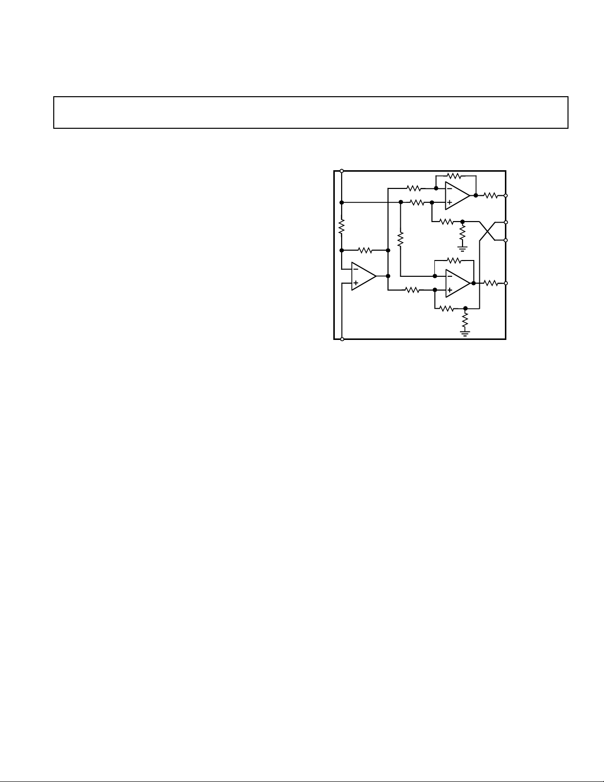
FUNCTIONAL BLOCK DIAGRAM
Based on a cross-coupled, electronically balanced topology, the
SSM2142 mimics the performance of fully balanced
transformer-based solutions for line driving. However, the
SSM2142 maintains lower distortion and occupies much less
board space than transformers while achieving comparable
common-mode rejection performance with reduced parts count.
The SSM2142 in tandem with the SSM2141 differential
receiver establishes a complete, reliable solution for driving and
receiving audio signals over long cables. The SSM2141 features
an Input Common-Mode Rejection Ratio of 100 dB at 60 Hz.
Specifications demonstrating the performance of this typical
system are included in the data sheet.
Information furnished by Analog Devices is believed to be accurate and
reliable. However, no responsibility is assumed by Analog Devices for its
use, nor for any infringements of patents or other rights of third parties
which may result from its use. No license is granted by implication or
otherwise under any patent or patent rights of Analog Devices.
Page 2
(VS = 618 V, –408C ≤ TA ≤ +858C, operating in differential mode unless otherwise
– FORCE
– SENSE
GROUND
V
IN
+ FORCE
+ SENSE
+V
–V
NC
NC
NC
NC
NC
NC
NC
NC
1
2
3
4
5
6
7
8
16
15
14
13
12
11
10
9
REV. C
–38
–35
SSM2142–SPECIFICATIONS
noted. Typical characteristics apply to operation at TA = +258C.)
Parameter Symbol Conditions Min Typ Max Units
INPUT IMPEDANCE Z
INPUT CURRENT I
IN
IN
VIN = ±7.071 V ±750 ±900 µA
10 kΩ
GAIN, DIFFERENTIAL 5.8 5.98 dB
GAIN, SINGLE-ENDED Single-Ended Mode 5.7 5.94 dB
GAIN ERROR, DIFFERENTIAL RL = 600 Ω 0.7 2 %
POWER SUPPLY REJECTION
RATIO STATIC PSRR VS = ±13 V to ±18 V 60 80 dB
OUTPUT COMMON-MODE REJECTION OCMR See Test Circuit; f = 1 kHz –45 dB
OUTPUT SIGNAL BALANCE RATIO SBR See Test Circuit; f = 1 kHz –40 dB
TOTAL HARMONIC DISTORTION
Plus Noise THD+N 20 Hz to 20 kHz, 0.006 %
VO = 10 V rms, RL = 600 Ω
SIGNAL-TO-NOISE RATIO SNR VIN = 0 V –93.4 dBu
HEADROOM HR CLIP Level = 10.5 V rms +93.4 dBu
SLEW RATE SR 15 V/µs
OUTPUT COMMON-MODE
VOLTAGE OFFSET
1
V
OOS
RL = 600 Ω –250 25 250 mV
DIFFERENTIAL OUTPUT
VOLTAGE OFFSET V
OOD
RL = 600 Ω –50 15 50 mV
DIFFERENTIAL OUTPUT
VOLTAGE SWING VIN = ±7.071 V ±13.8 ±14.14 V
OUTPUT IMPEDANCE Z
SUPPLY CURRENT I
OUTPUT CURRENT, SHORT CIRCUIT I
NOTES
1
Output common-mode offset voltage can be removed by inserting dc blocking capacitors in the sense lines. See Applications Information.
Specifications subject to change without notice.
SY
SC
O
Unloaded, VIN = 0 V 5.5 7.0 mA
45 50 55 Ω
60 70 mA
ABSOLUTE MAXIMUM RATINGS*
Supply Voltage . . . . . . . . . . . . . . . . . . . . . . . . . . . . . . . . ±18 V
Storage Temperature . . . . . . . . . . . . . . . . . . –60°C to +150°C
Lead Temperature (Soldering, 60 sec) . . . . . . . . . . . . +300°C
Junction Temperature . . . . . . . . . . . . . . . . . . . . . . . . +150°C
Operating Temperature Range . . . . . . . . . . . . –40°C to +85°C
Output Short Circuit Duration (Both Outputs) . . . . Indefinite
*Stresses above those listed under “Absolute Maximum Ratings” may cause
permanent damage to the device. These are stress ratings only; the functional
operation of the device at these or any other conditions above those indicated in the
operational sections of this specification is not implied. Exposure to absolute
maximum rating conditions for extended periods may affect device reliability.
–2–
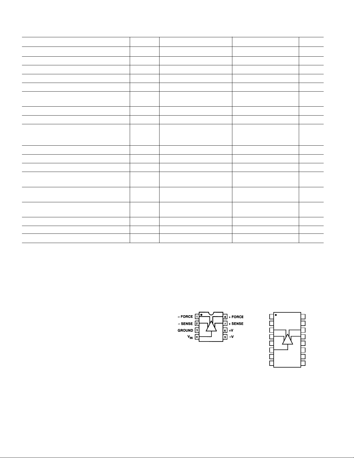
PIN CONNECTIONS
8-Pin Plastic DIP
(P Suffix)
16-Pin Wide Body SOL
(S Suffix)
Page 3
SSM2142
10
12
FREQUENCY – kHz
10
8
6
4
2
0
20 30 50 100
OUTPUT VOLTAGE SWING – V rms
T
A
= +25°C
V
S
= ±18V
R
L
= 600Ω
DIFF. MODE
0.1% DISTORTION
0.01% DISTORTION
±2
SUPPLY VOLTAGE – Volts
6.5
SUPPLY CURRENT – mA
±6 ±10 ±14 ±18
T
A
= +25°C
V
IN
= 0V
NO LOAD
6.0
5.5
5.0
4.5
4.0
3.5
300
300
600
+18V
–18V
V = 10V p–p
IN
∆V
OUT
V
IN
SBR = 20 LOG
V
OUT
2
1
3
4
5
6
7
8
V
Ω
Ω
Ω
REV. C
300Ω
V
OUT
V
300Ω
1
2
3
= 0V
V
S
4
OCMR = 20 LOG
8
7
+18V
6
–18V
5
V
= 10V p–p
CMR
∆V
OUT
V
CMR
600Ω
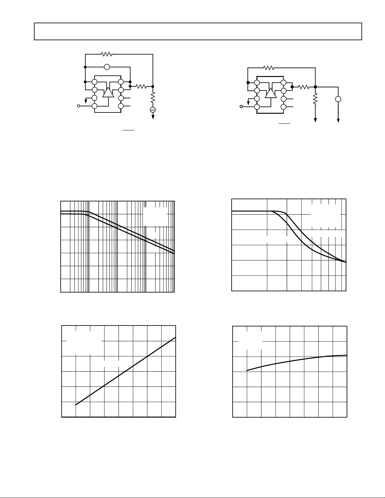
Figure 1. Output CMR Test Circuit
Typical Performance Characteristics
140
120
100
80
60
40
20
POWER SUPPLY REJECTION – dB
0
10
100 1k 10k 100k
FREQUENCY – Hz
Figure 3. Power Supply Rejection vs. Frequency
12
= +25°C
T
A
= 600Ω
R
L
10
DIFF. MODE
FREQ. = 20kHz
8
0.1% DISTORTION
6
TA = +25°C
= ±18V
V
S
∆V
= ±1V
S
–PSR
+PSR
Figure 2. Signal Balance Ratio (BBC Method) Test Circuit
Figure 4. Maximum Output Voltage Swing vs. Frequency
OUTPUT VOLTAGE SWING – V rms
Figure 5. Output Voltage Swing vs. Supply Voltage
4
2
0
±2
±6 ±10 ±14 ±18
SUPPLY VOLTAGE – Volts
Figure 6. Supply Current vs. Supply Voltage
–3–
Page 4

SSM2142
REV. C
THD PERFORMANCE
The following data, taken from the THD test circuit on an
Audio Precision System One using the internal 80 kHz noise
filter, demonstrates the typical performance of a balanced pair
system based on the SSM2142/SSM2141 chip set. Both differential and single-ended modes of operation are shown, under
a number of output load conditions which simulate various
application situations. Note also that there is no adverse effect
on system performance when using the optional series feedback
capacitors, which reject dc cable offsets in order to maintain
optimal ac noise rejection. The large signal transient response of
the system to a 100 kHz square wave input is also shown,
demonstrating the stability of the SSM2142 under load.
+18V
10µF*
6
4
V
IN
7
8
SSM
3
2142
1
2
5
10µF*
–18V
*USED ONLY IN THD PLOTS AS NOTED.
ALL CABLE MEASUREMENTS USE BELDEN 8451 CABLE.
A
C
R
L
R2
R1
SSM
B
2141
V
OUT
Figure 9. THD+N vs. Frequency at Point B
(Differential Mode)
Figure 7. THD Test Circuit
Figure 10. THD+N vs. Frequency at Point A
(Single Ended)
Figure 8. THD+N vs. Frequency at Point B
(Differential Mode)
Figure 11. THD+N vs. Frequency at Point C
(SSM2141 Output)
–4–
Page 5

100
REV. C
90
10
0%
Figure 12. 100 kHz Square Wave Observed at Point B
(Differential Mode). V
100
90
10
0%
= 10 V rms, R1 = R2 = ∞, RL = 600
O
Ω
Figure 13. 100 kHz Square Wave at Point B (Differential
Mode). V
= 10 V rms, R1 = R2 = ∞, RL = 600 Ω, with
O
Series Feedback Capacitors
+15V
+15V
6
4
V
IN
7
8
SSM
2142
3
–15V
1
2
5
SHIELDED
TWISTED-PAIR
CABLE
7
3
2
SSM
2141/
2143
–15V
5
V
OUT
6
1
4
Figure 14. Typical Application of the SSM2142 and
SSM2141
APPLICATIONS INFORMATION
The SSM2142 is designed to provide excellent common-mode
rejection, high output drive, and low signal distortion and noise
in a balanced line-driving system. The differential output stage
consists of twin cross-coupled unity gain buffer amplifiers with
SSM2142
on-chip 50 Ω series damping resistors. The impedances in the
output buffer pair are precisely balanced by laser trimming
during production. This results in the high gain accuracy
needed to obtain good common-mode noise rejection, and
excellent separation between the offset error voltages common
to the cable pair and the desired differential input signal. As
shown in the test circuit, it is suggested that a suitable balanced,
high input-impedance differential amplifier such as the
SSM2141 be used at the receiving end for best system
performance. The SSM2141 receiver output is configured for a
gain of one half following the 6 dB gain of the SSM2142, in
order to maintain an overall system gain of unity.
In applications encountering a large dc offset on the cable or
those wishing to ensure optimal rejection performance by
avoiding differential offset error sources, dc blocking capacitors
may be employed at the sense outputs of the SSM2142. As
shown in the test circuit, these components should present as
little impedance as possible to minimize low-frequency errors,
such as 10 µF NP (or tantalum if the polarity of the offset is
known).
SYSTEM GROUNDING CONSIDERATIONS
Due to ground currents, supply variations, and other factors,
the ground potentials of the circuits at each end of a signal cable
may not be exactly equal. The primary purpose of a balanced
pair line is to reject this voltage difference, commonly called
“longitudinal error.” A measure of the ability of the system to
reject longitudinal error voltage is output common-mode
rejection. In order to obtain the optimal OCMR and noise
rejection performance available with the SSM2142, the user
should observe the following precautions:
1. The quality of the differential output is directly dependent
upon the accuracy of the input voltage presented to the
device. Input voltage errors developed across the impedance
of the source must be avoided in order to maintain system
performance. The input of the SSM2142 should be driven
directly by an operational amplifier or buffer offering low
source impedance and low noise.
2. The ground input should be in close proximity to the singleended input’s source common. Ground offset errors encountered in the source circuitry also impair system performance.
3. Make sure that the SSM2142 is adequately decoupled with
0.1 µF bypass capacitors located close to each supply pin.
4. Avoid the use of passive circuitry in series with the SSM2142
outputs. Any reactive difference in the line pair will cause
significant imbalances and affect the gain error of the device.
Snubber networks or series load resistors are not required to
maintain stability in SSM2142 based systems, even when
driving signals over extremely long cables.
5. Efforts should be made to maintain a physical balance in the
arrangement of the signal pair wiring. Capacitive differences
due to variations in routing or wire length may cause unequal
noise pickup between the pair, which will degrade the system
OCMR. Shielded twisted-pair cable is the preferred choice in
all applications. The shield should not be utilized as a signal
conductor. Grounding the shield at one end, near the output
common, avoids ground loop currents flowing in the shield
which increase noise coupling and longitudinal errors.
–5–
Page 6

SSM2142
REV. C
THE CABLE PAIR
The SSM2142 is capable of driving a 10 V rms signal into
600 Ω and will remain stable despite cable capacitances of up to
0.16 µF in either balanced or single-ended configurations. Low
impedance shielded audio cable such as the standard Belden
8451 or similar is recommended, especially in applications
traversing considerable distances. The user is cautioned that the
so-called “audiophile” cables may incur four times the capacitance per unit length of the standard industrial-grade product.
In situations of extreme load and/or distance, adding a second
parallel cable allows the user to trade off half of the total line
resistance against a doubling in capacitive load.
SINGLE-ENDED OPERATION
The SSM2142 is designed to be compatible with existing
balanced-pair interface systems. Just as in transformer-based
circuits, identical but opposite currents are generated by the
output pair which can be ground-referenced if desired and
transmitted on a single wire. Single-ended operation requires
that the unused side of the output pair be grounded to a solid
return path in order to avoid voltage offset errors at the nearby
input common. The signal quality obtained in these systems is
directly dependent on the quality of the ground at each end of
the wire. Also note that in single-ended operation the gain
through the device is still 6 dB, and that the SSM2142 incurs
no significant degradation in signal distortion or output drive
capability, although the noise rejection inherent in balancedpair systems is lost.
POWER SUPPLY SEQUENCING
A problem occasionally encountered in the interface system environment involves irregular application of the supplies. The
user is cautioned that applying power erratically can inadvertently bias parts of the circuit into a latch-up condition. The
small geometries of an integrated circuit are easily breached and
damaged by short-risetime spikes on a supply line, which usually demonstrate considerable overshoot. The questionable
practice of exchanging components or boards while under
power can create such an undesirable sequence as well. Possible
options which offer improved board-level device protection
include: additional bypass capacitors, high-current reversebiased steering diodes between both supplies and ground, various transient surge suppression devices, and safety grounding
connectors.
Likewise, power should be applied to the device before the
output is connected to “live” systems which may carry voltages
of sufficient magnitude to turn on the output devices of the
SSM2142 and damage the device. In any case, of course, the
user must always observe the absolute maximum ratings shown
in the specifications.
PRINTED IN U.S.A.
–6–
Page 7

SSM2142
C
OUTLINE DIMENSIONS
0.400 (10.16)
0.365 (9.27)
0.355 (9.02)
0.210 (5.33)
0.150 (3.81 )
0.130 (3.30 )
0.115 (2.92)
0.022 (0.5 6)
0.018 (0.4 6)
0.014 (0.3 6)
MAX
8
1
0.100 (2.5 4)
0.070 (1.7 8)
0.060 (1.5 2)
0.045 (1.1 4)
BSC
5
4
0.280 (7. 11)
0.250 (6.35)
0.240 (6.10)
0.015
(0.38)
MIN
SEATING
PLANE
0.005 (0.13)
MIN
0.060 (1.5 2)
MAX
0.015 (0.3 8)
GAUGE
PLANE
0.325 (8.2 6)
0.310 (7.8 7)
0.300 (7.6 2)
0.430 (10.92)
MAX
0.195 (4.95 )
0.130 (3.30 )
0.115 (2.92)
0.014 (0.36)
0.010 (0.25)
0.008 (0.20)
CONTROLLING DIMENSIONSARE IN INCHES ; MILLIMETER DIMENSIONS
(IN PARENTHESES) ARE ROUNDED-O FF INCH EQUIVALENTS FOR
REFERENCE ONLYAND ARE NOT APPROPRIATE FOR USE IN DESIGN.
CORNER LEADS MAY BE CONFIGURED AS WHOLE OR HALF LEADS.
COMPLIANT TO JED EC STANDARDS MS - 001
070606-A
Figure 1. 8-Lead Plastic Dual In-Line Package [PDIP]
Narrow Body
(N-8)
Dimensions shown in inches and (millimeters)
10.50 (0.4134)
10.10 (0.3976)
BSC
9
7.60 (0.2992)
7.40 (0.2913)
8
10.65 (0.4193)
10.00 (0.3937)
2.65 (0.1043)
2.35 (0.0925)
SEATING
PLANE
8°
0°
0.33 (0.0130)
0.20 (0.0079)
0
0
.
7
.
2
(
5
0
(
5
0
)
.
0
2
9
5
)
.
0
0
9
8
1.27 (0.0500)
0.40 (0.0157)
45°
03-27-2007-B
0.30 (0.0118)
0.10 (0.0039)
OPLANARITY
0.10
16
1
1.27 (0.0500)
0.51 (0.0201)
0.31 (0.0122)
CONTROLLING DIMENSIONS ARE IN MILLIMETERS; INCH DIMENSIONS
(IN PARENTHESES) ARE ROUNDED-OFF MILLIMETER EQUIVALENTS FOR
REFERENCE ONLY AND ARE NOT APPROPRIATE FOR USE IN DESIGN.
COMPLIANT TO JEDEC STANDARDS MS-013-AA
Figure 2. 16-Lead Standard Small Outline Package [SOIC_W]
Wide Body
(RW-16)
Dimensions shown in millimeters and (inches)
ORDERING GUIDE
Model1 Temperature Range Package Descriptions Package Option
SSM2142PZ −40°C to +85°C 8-Lead PDIP N-8
SSM2142SZ −40°C to +85°C 16-Lead SOIC_W RW-16
SSM2142SZ-REEL −40°C to +85°C 16-Lead SOIC_W RW-16
1
Z = RoHS Compliant Part.
Rev. C | Page 7 of 8
Page 8

SSM2142
REVISION HISTORY
5/11—Rev. B to Rev. C
Changes to Output Common-Mode Rejection Parameter and
Output Signal Balance Ratio Parameter in
SSM2142—Specifications Table ...................................................... 2
Updated Outline Dimensions ......................................................... 7
Changes to Ordering Guide ............................................................ 7
©1991–2011 Analog Devices, Inc. All rights reserved. Trademarks and
registered trademarks are the property of their respective owners.
D01496-0-5/11(C)
Rev. C | Page 8 of 8
 Loading...