

Page 1
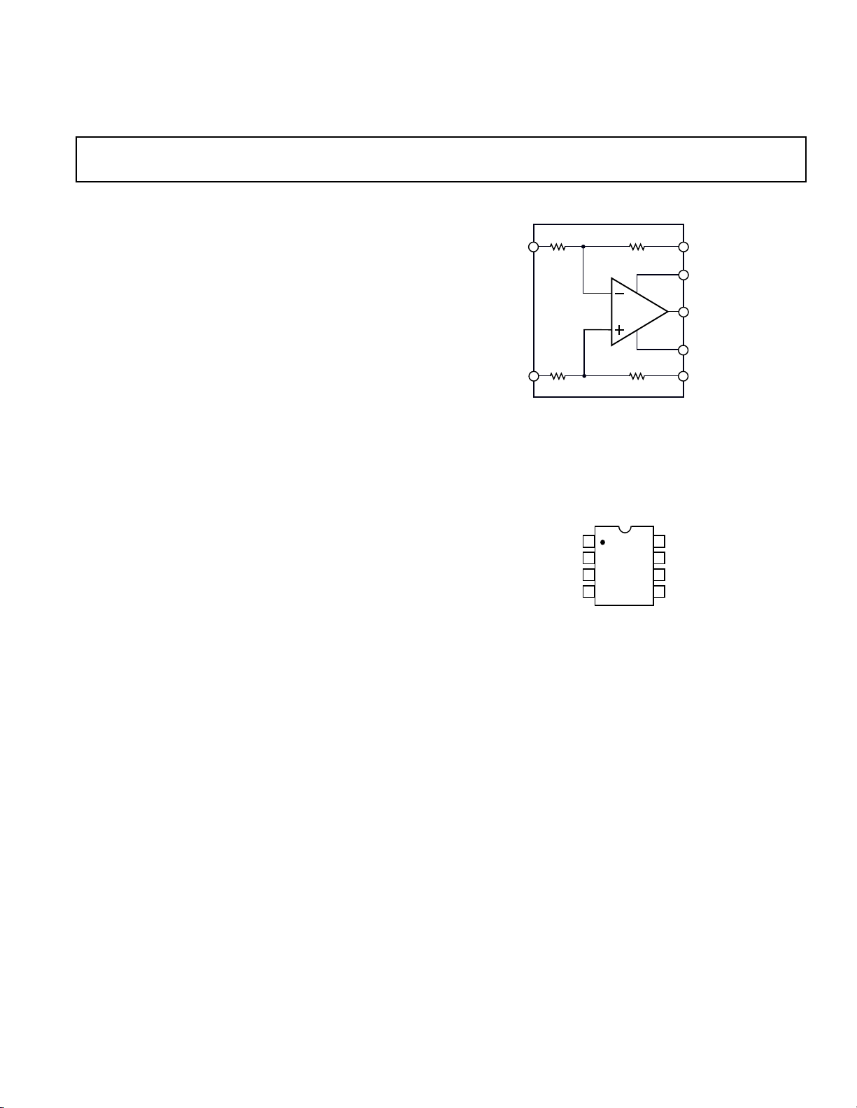
SSM2141
–IN
+IN
SENSE
+V
CC
OUTPUT
–V
EE
REFERENCE
25kΩ 25kΩ
25kΩ25kΩ
1
3
2
5
7
6
4
1
2
3
4
8
7
6
5
TOP VIEW
(Not to Scale)
NC = NO CONNECT
SSM2141
REFERENCE
SENSE
OUTPUT
V+
NC
–IN
+IN
V–
High Common-Mode Rejection
C
781/461-3113
a
FEATURES
High Common-Mode Rejection
DC: 100 dB typ
60 Hz: 100 dB typ
20 kHz: 70 dB typ
40 kHz: 62 dB typ
Low Distortion: 0.001% typ
Fast Slew Rate: 9.5 V/ms typ
Wide Bandwidth: 3 MHz typ
Low Cost
Complements SSM2142 Differential Line Driver
APPLICATIONS
Line Receivers
Summing Amplifiers
Buffer Amplifiers–Drives 600 V Load
GENERAL DESCRIPTION
The SSM2141 is an integrated differential amplifier intended to
receive balanced line inputs in audio applications requiring a
high level of noise immunity and optimum common-mode
rejection. The SSM2141 typically achieves 100 dB of commonmode rejection (CMR), whereas implementing an op amp with
four off-the-shelf precision resistors will typically achieve only
40 dB of CMR—inadequate for high-performance audio.
The SSM2141 achieves low distortion performance by
maintaining a large slew rate of 9.5 V/µs and high open-loop
gain. Distortion is less than 0.002% over the full audio
bandwidth. The SSM2141 complements the SSM2142
balanced line driver. Together, these devices comprise a fully
integrated solution for equivalent transformer balancing of
audio signals without the problems of distortion, EMI fields,
and high cost.
Additional applications for the SSM2141 include summing
signals, differential preamplifiers, and 600 Ω low distortion
buffer amplifiers. For similar performance with G = 1/2, see
SSM2143.
Differential Line Receiver
SSM2141
FUNCTIONAL BLOCK DIAGRAM
PIN CONNECTIONS
8-Pin Plastic Mini-DIP
(P Suffix)
Narrow Body SO
(S Suffix)
REV.
Information furnished by Analog Devices is believed to be accurate and
reliable. However, no responsibility is assumed by Analog Devices for its
use, nor for any infringements of patents or other rights of third parties
which may result from its use. No license is granted by implication or
otherwise under any patent or patent rights of Analog Devices.
One Technology Way, P.O. Box 9106, Norwood, MA 02062-9106, U.S.A.
Tel: 617/329-4700 Fax:
Page 2
SSM2141–SPECIFICA TIONS
C
ELECTRICAL CHARACTERISTICS
(@ VS = 618 V, TA = +258C, unless otherwise noted)
SSM2141
Parameter Symbol Conditions Min Typ Max Units
OFFSET VOLTAGE V
OS
VCM = 0 V –1000 25 1000 µV
GAIN ERROR No Load, VIN = ±10 V, RS = 0 Ω 0.001 0.01 %
INPUT VOLTAGE RANGE IVR (Note 1) ±10 V
COMMON-MODE REJECTION CMR VCM = ±10 V 80 100 dB
POWER SUPPLY REJECTION RATIO PSRR VS = ±6 V to ±18 V 0.7 15 µV/V
OUTPUT SWING V
SHORT-CIRCUIT CURRENT LIMIT I
O
SC
RL = 2 kΩ±13 ±14.7 V
Output Shorted to Ground +45/–15 mA
SMALL-SIGNAL BANDWIDTH (–3 dB) BW RL = 2 kΩ 3 MHz
SLEW RATE SR RL = 2 kΩ 6 9.5 V/µs
TOTAL HARMONIC DISTORTION R
= 100 kΩ 0.001 %
L
THD RL = 600 Ω 0.01
CAPACITIVE LOAD DRIVE CAPABILITY C
SUPPLY CURRENT I
NOTES
1
Input Voltage Range Guaranteed by CMR test.
Specifications subject to change without notice
L
SY
No Oscillation 300 pF
No Load 2.5 3.5 mA
ELECTRICAL CHARACTERISTICS
(@ VS = 618 V, –408C ≤ TA ≤ +858C)
Parameter Symbol Conditions Min Typ Max Units
OFFSET VOLTAGE V
OS
VCM = 0 V –2500 200 2500 µV
GAIN ERROR No Load, VIN = ±10 V, RS = 0 Ω 0.002 0.02 %
INPUT VOLTAGE RANGE IVR (Note 1) ±10 V
COMMON-MODE REJECTION CMR VCM = ±10 V 75 90 dB
POWER SUPPLY REJECTION RATIO PSRR VS = ±6 V to ±18 V 1.0 20 µV/V
OUTPUT SWING V
O
RL = 2 kΩ±13 ±14.7 V
SLEW RATE SR RL = 2 kΩ 9.5 V/µs
SUPPLY CURRENT I
NOTES
1
Input Voltage Range Guaranteed by CMR test.
Specifications subject to change without notice
SY
No Load 2.6 4.0 mA
–2–
REV.
Page 3
SSM2141
C
ABSOLUTE MAXIMUM RATINGS
Supply Voltage . . . . . . . . . . . . . . . . . . . . . . . . . . . . . . . ±18 V
Input Voltage
1
. . . . . . . . . . . . . . . . . . . . . . . . Supply Voltage
1
Output Short-Circuit Duration . . . . . . . . . . . . . . Continuous
Storage Temperature Range
P Package . . . . . . . . . . . . . . . . . . . . . . . –65°C to +150°C
Lead Temperature (Soldering, 60 sec) . . . . . . . . . . . . +300°C
Junction Temperature . . . . . . . . . . . . . . . . . . . . . . . . +150°C
Operating Temperature Range . . . . . . . . . . . . –40°C to +85°C
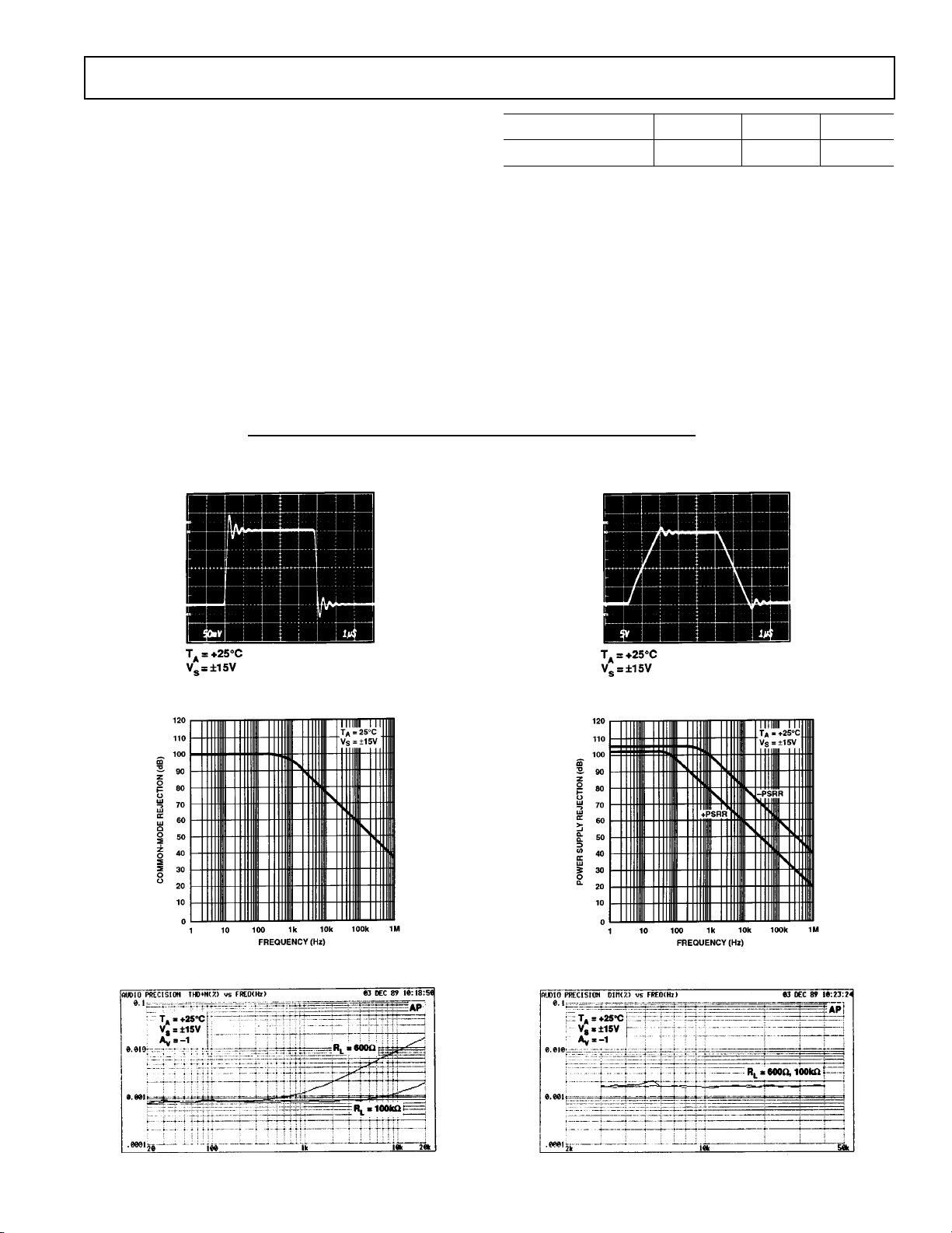
Typical Performance Characteristics
Package Type u
2
JA
u
JC
Units
8-Pin Plastic DIP (P) 103 43 °C/W
NOTES
1
For supply voltages less than ±18 V, the absolute maximum input voltage is equal
to the supply voltage.
2
θJA is specified for worst case mounting conditions, i.e., θJA is specified for device
in socket for P-DIP package.
Small Signal Transient Response
Common-Mode Rejection vs. Frequency
Large Signal Transient Response
Power Supply Rejection vs. Frequency
REV.
Total Harmonic Distortion vs. Frequency
–3–
Dynamic Intermodulation Distortion vs. Frequency
Page 4

SSM2141–
C
Typical Performance Characteristics
Input Offset Voltage vs. Temperature
Gain Error vs. Temperature
Closed-Loop Gain vs. Frequency
Slew Rate vs. Temperature
Closed-Loop Output Impedance
vs. Frequency
Supply Current vs. Temperature
Supply Current vs. Supply Voltage
Maximum Output Voltage vs.
Output Current (Source)
Maximum Output Voltage vs.
Output Current (Sink)
REV. –4–
Page 5

SSM2141
5mV
1S
+1µV
0V
–1µV
0.1 TO 10Hz PEAK-TO-PEAK NOISE
10mV
2mS
+10µV
0V
–10µV
NOTE: EXTERNAL AMPLIFIER GAIN = 1000;
THEREFORE, VERTICAL SCALE = 10µV/DIV.
TA = +25°C
V
S
= ±15V
C
Voltage Noise Density vs. Frequency
10mV
TA = +25°C
V
= ±15V
S
NOTE: EXTERNAL AMPLIFIER GAIN = 1000;
THEREFORE, VERTICAL SCALE = 10µV/DIV.
1mS
+10µV
0V
–10µV
Voltage Noise from 0 kHz to 1 kHz
APPLICATIONS INFORMATION
The SSM2141 represents a versatile analog building block. In
order to capitalize on fast settling time, high slew rate, and high
CMR, proper decoupling and grounding techniques must be
employed. For decoupling, place 0.1 µF capacitor located within
close proximity from each supply pin to ground.
Low Frequency Voltage Noise
Voltage Noise from 0 kHz to 10 kHz
REV.
Slew Rate Test Circuit
–5–
Page 6

SSM2141
C
MAINTAINING COMMON-MODE REJECTION
In order to achieve the full common-mode rejection capability
of the SSM2141, the source impedance must be carefully
controlled. Slight imbalances of the source resistance will result
in a degradation of DC CMR—even a 5 Ω imbalance will
degrade CMR by 20 dB. Also, the matching of the reactive
source impedance must be matched in order to preserve the
CMRR over frequency.
Figure 1. Precision Difference Amplifier. Rejects
[E
+
E2]
Common-Mode Signal =
1
2
by 100 dB
Figure 5. Suitable Instrumentation Amplifier
Requirements can be Addressed by Using an
Input Stage Consisting of A1, A2, R1 and R
2
Figure 2. Precision Unity Gain Inverting Amplifier
Figure 3. Precision Summing Amplifier
Figure 4. Precision Summing Amplifier with Gain
–6–
REV.
Page 7

SSM2141
OUTLINE DIMENSIONS
0.400 (10.16)
0.365 (9.27)
0.355 (9.02)
0.210 (5.33)
0.150 (3.81)
0.130 (3.30)
0.115 (2.92)
0.022 (0.56)
0.018 (0.46)
0.014 (0.36)
MAX
8
1
0.100 (2.54)
0.070 (1.78)
0.060 (1.52)
0.045 (1.14)
BSC
5
4
0.280 (7.11)
0.250 (6.35)
0.240 (6.10)
0.015
(0.38)
MIN
SEATING
PLANE
0.005 (0.13)
MIN
0.060 (1.52)
MAX
0.015 (0.38)
GAUGE
PLANE
0.325 (8.26)
0.310 (7.87)
0.300 (7.62)
0.430 (10.92)
MAX
0.195 (4.95)
0.130 (3.30)
0.115 (2.92)
0.014 (0.36)
0.010 (0.25)
0.008 (0.20)
CONTROLL ING DIMENSIONS ARE IN INCHES; M I LLIMETER DIMENSIONS
(IN PARENTHESES) ARE ROUNDED-OFF INCH EQUI VALENTS FOR
REFERENCE ON LY AND ARE NOT APPROP RIATE FOR USE IN DESIGN.
CORNER LEADS MAY BE CONFIGURED AS WHO L E O R HAL F L EADS .
COMPLIANT TO JEDEC STANDARDS MS-001
070606-A
Figure 6. 8-Lead Plastic Dual In-Line Package [PDIP]
Narrow Body
(N-8)
Dimensions shown in inches and (millimeters)
5.00(0.1968)
4.80(0.1890)
4.00 (0.1574)
3.80 (0.1497)
0.25 (0.0098)
0.10 (0.0040)
COPLANARITY
0.10
CONTROLLING DIMENSIONS ARE IN MILLIMETERS; INCH DIMENSIONS
(IN PARENTHESES)ARE ROUNDED-OFF MILLIMETER EQUIVALENTS FOR
REFERENCE ONLYAND ARE NOT APPROPRIATE FOR USE IN DESIGN.
85
1
1.27 (0.0500)
SEATING
PLANE
COMPLIANT TO JEDEC STANDARDS MS-012-AA
BSC
6.20 (0.2441)
5.80 (0.2284)
4
1.75 (0.0688)
1.35 (0.0532)
0.51 (0.0201)
0.31 (0.0122)
8°
0°
0.25 (0.0098)
0.17 (0.0067)
0.50 (0.0196)
0.25 (0.0099)
1.27 (0.0500)
0.40 (0.0157)
45°
012407-A
Figure 7.8-Lead Standard Small Outline Package [SOIC_N]
Narrow Body
(R-8)
Dimensions shown in millimeters and (inches)
REV. C –7–
Page 8

SSM2141
ORDERING GUIDE
Model1 Temperature Range Package Description Package Option
SSM2141PZ −40°C ≤ TA ≤ +85°C 8-Lead PDIP N-8
SSM2141SZ −40°C ≤ TA ≤ +85°C 8-Lead SOIC_N R-8
SSM2141SZ-REEL −40°C ≤ TA ≤ +85°C 8-Lead SOIC_N R-8
1
Z = RoHS Compliant Part.
REVISION HISTORY
6/11—Rev. B to Rev. C
Updated Outline Dimensions ......................................................... 7
Changes to Ordering Guide ............................................................ 8
5/91—Rev. A to Rev. B
©2007 Analog Devices, Inc. All rights reserved. Trademarks and
registered trademarks are the property of their respective owners.
D10008-0-6/11(C)
–8– REV. C
 Loading...