

Page 1

TABLE OF CONTENTS
GENERAL DESCRIPTION.................................................................................................................1
1
2 FEATURES ........................................................................................................................................2
3 ORDERING INFORMATION..............................................................................................................2
4 BLOCK DIAGRAM.............................................................................................................................3
5 DIE ARRANGEMENT ........................................................................................................................4
6 PIN DESCRIPTION ............................................................................................................................9
6.1 RES#............................................................................................................................................9
6.2 PS0 ..............................................................................................................................................9
6.3 PS1 ..............................................................................................................................................9
6.4 CS#..............................................................................................................................................9
6.5 D/C#.............................................................................................................................................9
6.6 R/W(WR#)....................................................................................................................................9
6.7 E(RD#).........................................................................................................................................9
6.8 D0 -D7...........................................................................................................................................9
6.9 VDD...............................................................................................................................................9
6.10 RVSS...........................................................................................................................................10
6.11 CVSS...........................................................................................................................................10
6.12 VSS.............................................................................................................................................10
6.13 VCI..............................................................................................................................................10
6.14 V
6.15 V
.............................................................................................................................................10
out
L5, VL4, VL3
and VL2...................................................................................................................10
6.16 COM0 – COM63........................................................................................................................10
6.17 ICONS........................................................................................................................................10
6.18 COL0 – COL103........................................................................................................................10
i
Page 2

6.19
CL..............................................................................................................................................10
6.20 M................................................................................................................................................11
6.21 MID0~MID2................................................................................................................................11
6.22 SYNC.........................................................................................................................................11
6.23 MODE........................................................................................................................................11
6.24 TEST_IN0~1..............................................................................................................................11
6.25 TEST0~14..................................................................................................................................11
6.26 N/C.............................................................................................................................................11
6.27 Dummy......................................................................................................................................11
7 FUNCTIONAL BLOCK DESCRIPTIONS ........................................................................................12
7.1 Command Decoder and Command Interface........................................................................12
7.2 MPU Parallel 6800-series Interface ........................................................................................12
7.3 MPU Parallel 8080-series Interface ........................................................................................12
7.4 MPU Serial 4-wire Interface.....................................................................................................13
7.5 MPU Serial 3-wire interface.....................................................................................................13
7.6 Graphic Display Data RAM (GDDRAM)..................................................................................13
7.7 Oscillator Circuit......................................................................................................................13
7.8 LCD Driving Voltage Generator and Regulator....................................................................14
7.9 169 Bit Latch ............................................................................................................................14
7.10 Level selector...........................................................................................................................14
7.11 HV Buffer Cell (Level Shifter)..................................................................................................14
7.12 Default Setting after Reset......................................................................................................15
7.13 LCD Panel Driving Waveform................................................................................................. 16
COMMAND TABLE....................................................................................................................................20
7.14 Read Status Byte .....................................................................................................................25
7.15 Data Read / Write .....................................................................................................................25
8 COMMAND DESCRIPTIONS ..........................................................................................................26
ii
Page 3

8.1
Set Display On/Off ...................................................................................................................26
8.2 Set Display Start Line..............................................................................................................26
8.3 Set Page Address ....................................................................................................................26
8.4 Set Higher Column Address...................................................................................................26
8.5 Set Lower Column Address....................................................................................................26
8.6 Set Temperature Coefficient (TC) Value................................................................................26
8.7 Set Segment Re-map...............................................................................................................26
8.8 Set Normal/Reverse Display...................................................................................................26
8.9 Set Entire Display On/Off........................................................................................................26
8.10 Set LCD Bias ............................................................................................................................26
8.11 Software Reset.........................................................................................................................27
8.12 Set COM Output Scan Direction.............................................................................................27
8.13 Set Power Control Register ....................................................................................................27
8.14 Set Internal Regulator Resistors Ratio..................................................................................27
8.15 Set Contrast Control Register ................................................................................................28
8.16 Set frame frequency ................................................................................................................29
8.17 Set Multiplex Ratio...................................................................................................................29
8.18 Set Power Save Mode..............................................................................................................29
8.19 Exit Power Save Mode.............................................................................................................29
8.20 Set N-line Inversion .................................................................................................................29
8.21 Exit N-line Inversion ................................................................................................................29
8.22 Set DC-DC Converter Factor...................................................................................................29
8.23 Set Icon Enable........................................................................................................................29
8.24 Start Internal Oscillator...........................................................................................................29
8.25 Set Display Data Length..........................................................................................................29
8.26 Set Test Mode ..........................................................................................................................29
8.27 Status register Read................................................................................................................30
8.28 Set Gray Scale Mode (White/Light Gray/Dark Gray/Black)..................................................30
iii
Page 4

8.29
Set PWM and FRC....................................................................................................................30
EXTENDED COMMANDS.....................................................................................................................30
8.30 OTP setting and programming...............................................................................................31
8.31 Enable External Oscillator Input ............................................................................................33
9 MAXIMUM RATINGS.......................................................................................................................34
10 DC CHARACTERISTICS .................................................................................................................35
11 AC CHARACTERISTICS .................................................................................................................37
12 APPLICATION EXAMPLES ............................................................................................................44
iv
Page 5

TABLE OF FIGURES
Figure 1 - Block Diagram .............................................................................................................................. 3
Figure 2 – SSD1858 Pin Assignment ........................................................................................................... 4
Figure 3 – Display Data Read with the insertion of Dummy Read.............................................................. 12
Figure 4 - Oscillator Circuitry.......................................................................................................................13
Figure 5 - SSD1858 Graphic Display Data RAM (GDDRAM) Address Map (with vertical scroll value 30H &
MODE=L) ............................................................................................................................................. 17
Figure 6 - SSD1858 Graphic Display Data RAM (GDDRAM) Address Map (with vertical scroll value 30H &
MODE=H) ............................................................................................................................................18
Figure 7 - LCD Display Example “0” ........................................................................................................... 19
Figure 8 - LCD Driving Signal from SSD1858............................................................................................. 19
Figure 9 - Contrast Control Voltage Range Curve (TC=-0.14%/oC; VDD=2.775V; V
=3.5V) .....................28
CI
Figure 10 - Contrast Control Flow...............................................................................................................28
Figure 11 - OTP programming circuitry....................................................................................................... 31
Figure 12 - Flow chart of OTP program ...................................................................................................... 32
Figure 13 - Frame Frequency at different VDD( Temp = 25
o
C).................................................................. 37
Figure 14 – Parallel 6800-series Interface Timing Characteristics (PS0 = H, PS1 = H)............................. 38
Figure 15 - Parallel 6800-series Interface Timing Characteristics (PS0 = H, PS1 = H) .............................39
Figure 16 - Parallel 8080-series Interface Timing Characteristics (PS0 = H, PS1 = L) .............................. 40
Figure 17 - Parallel 8080-series Interface Timing Characteristics (PS0 = H, PS1 = L) .............................. 41
Figure 18- Serial Timing Characteristics (PS0 = L) .................................................................................... 42
Figure 19 - Serial Timing Characteristics (PS0 = L) ................................................................................... 43
LIST OF TABLE
Table 1 - Ordering Information......................................................................................................................2
Table 2 - SSD1858 Series Die Pad Coordinates .......................................................................................... 5
Table 3 - PS0 & PS1 Interface......................................................................................................................9
Table 4 - V
> VL5 > VL4 > VL3 > VL2 > V
out
Relationship ............................................................................ 10
SS
Table 5 – Mode setting................................................................................................................................11
Table 6 -Modes of Operation ......................................................................................................................13
Table 7 - COMMAND TABLE......................................................................................................................20
Table 8 – Extended Command Table ......................................................................................................... 24
Table 9 - Read Status Byte......................................................................................................................... 25
Table 10 - Address Increment Table........................................................................................................... 25
Table 11 - Commands Required for R/W (WR#) Actions on RAM ............................................................. 25
Table 12 - Maximum Ratings (Voltage Referenced to V
) ........................................................................ 34
SS
Table 13 - DC Characteristics (Unless otherwise specified, Voltage Referenced to VSS, VDD = 1.8 to 3.3V,
= -40 to 85°°°°C).................................................................................................................................. 35
T
A
Table 14 - AC Characteristics (Unless otherwise specified, Voltage Referenced to VSS, V
DD, VCI
= 2.7V, TA
= -40 to 85°°°°C) ......................................................................................................................................37
Table 15 – Parallel Timing Characteristics (T
Table 16 – Parallel Timing Characteristics (T
Table 17 - Parallel Timing Characteristics (T
Table 18 - Parallel Timing Characteristics (T
Table 19 – Serial Timing Characteristics (T
Table 20 – Serial Timing Characteristics (T
= -40 to 85°°°°C, V
A
= -40 to 85°°°°C, V
A
= -40 to 85°C, V
A
= -40 to 85°C, V
A
= -40 to 85°°°°C, V
A
= -40 to 85°°°°C, V
A
= 1.8V, V
DD
= 2.7, V
DD
= 1.8V, V
DD
= 2.7V, V
DD
= 2.7V, V
DD
= 1.8V, V
DD
=0V) ................................. 38
SS
=0V).................................... 39
SS
=0V) .................................. 40
SS
=0V) .................................. 41
SS
=0V) .................................... 42
SS
=0V) .................................... 43
SS
v
Page 6

SOLOMON SYSTECH LIMITED
SOLOMON SYSTECH LIMITED
SOLOMON SYSTECH LIMITEDSOLOMON SYSTECH LIMITED
SEMICONDUCTOR TECHNICAL DATA
SSD1858
Advanced Information
LCD Segment / Common Driver with Controller
CMOS
1 General Description
SSD1858 is a single-chip CMOS 4 gray scale LCD driver with controller for liquid crystal dot-matrix
graphic display system. SSD1858 consists of 169 high voltage driving output pins for driving maximum
104 Segments, 64 Commons and 1 icon driving Commons. SSD1858 supports two display modes 96x65
or 104x65 by pin select.
SSD1858 displays data directly from its internal 104x65x2 bits Graphic Display Data RAM
(GDDRAM). Data/Commands are sent from general MCU through a hardware selectable 6800-/8080series compatible Parallel Interface or 3/4 wires Serial Peripheral Interface
SSD1858 embeds a DC-DC Converter, a LCD Voltage Regulator, an On-Chip Bias Divider,
integrated bias capacitors, integrated booster capacitors and an On-Chip oscillator which reduce the
number of external components. With the special design on minimizing power consumption and
die/package layout, SSD1858 is suitable for any portable battery-driven applications requiring a long
operation period and a compact size.
.
This document contains information on a new product. Specifications and information herein are subject to change without
notice.
Copyright 2002 SOLOMON Systech Limited
Rev 1.1
09/2002
Page 7

2 FEATURES
104x64 4 gray scale levels Graphic Display with an Icon Line
Programmable Multiplex ratio (partial display) [16Mux - 65Mux]
Single Supply Operation, 1.8 V - 3.3V
Low Current Sleep Mode (<1.0uA)
On-Chip Voltage Generator / External Power Supply
Software selectable 2X / 3X / 4X / 5X On-Chip DC-DC Converter, with Integrated Capacitors
On-Chip Oscillator
Software Selectable On-Chip Bias Dividers, with Integrated Capacitors
Programmable 1/4, 1/5, 1/6, 1/7, 1/8, 1/9 bias ratio
Maximum +12.0V LCD Driving Output Voltage
Hardware pin selectable for 8-bit 6800-series Parallel Interface, 8-bit 8080-series Parallel
Interface, 3-wire Serial Peripheral Interface or 4-wire Serial Peripheral Interface
On-Chip 104 x 65 x 2 Graphic Display Data RAM
Re-mapping of Row and Column Drivers
Vertical Scrolling
Display Offset Control
64 Levels Internal Contrast Control
External Contrast Control
Maximum 17MHz SPI or 15MHz PPI operation
Selectable LCD Driving Voltage Temperature Coefficients (5 settings) [-0.14%/
o
C (POR)]
Programmable Frame Frequency
One time programmable (OTP) capability for Vout adjusts.
3 ORDERING INFORMATION
Table 1 - Ordering Information
Ordering Part Number Seg Com Package Form
SSD1858Z 104 /96 64 + 1 Gold Bump Die
SSD1858
Rev 1.1
09/2002
SOLOMON
2
Page 8
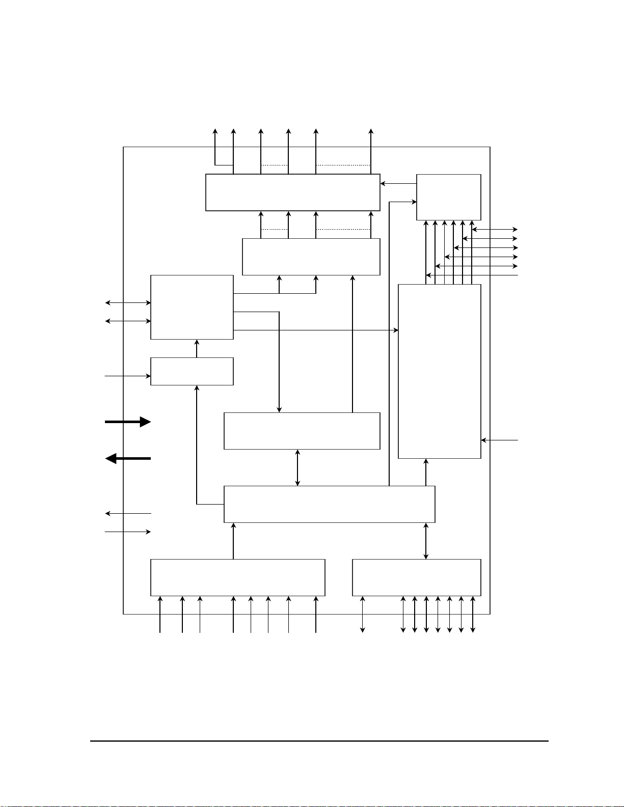
4 BLOCK DIAGRAM
M
SYNC
CL
TEST_IN0~1
TEST0~14
V
SS
V
DD
Display Timing
Generator
Oscillator
RES# PS0 PS1 CS# D/C# R/W E MODE
(WR#) (RD#)
ICONS COL0~COL103
Command Interface
COM0 to
COM63
HV Buffer Cell Level Shifter
169 Bit Latch
104 X 65 X 2 Bits
Command Decoder
LCD Driving
Voltage Generator
2X / 3X / 4X / 5X
DC/DC Converter,
Voltage Regulator,
Bias Divider,
Contrast Control,
Compensation
Parallel / Serial Interface
D
7 D6
(SDA) (SCK)
D5 D4 D
Level Selector
Vout
VL5
VL4
VL3
VL2
Vss
Temperature
VCI
3 D2 D1 D0
3
SSD1858
Rev 1.1
09/2002
Figure 1 - Block Diagram
SOLOMON
Page 9

I
5 DIE ARRANGEMENT
188
Pad355
DUMMY
DUMMY
DUMMY
DUMMY
DUMMY
DUMMY
DUMMY
DUMMY
DUMMY
DUMMY
DUMMY
DUMMY
DUMMY
DUMMY
DUMMY
DUMMY
DUMMY
DUMMY
DUMMY
DUMMY
DUMMY
DUMMY
DUMMY
DUMMY
DUMMY
DUMMY
DUMMY
DUMMY
COM16
COM15
:
:
:
:
COM1
COM0
ICONR
COL0
COL1
:
:
:
:
:
:
:
:
:
:
COL102
COL103
COM32
COM33
:
:
:
:
COM48
COM49
DUMMY
KEY4
DUMMY
COM17
COM18
KEY3
Centre: 5344.35, 237.9
Centre: -5349.9, 237.9
DUMMY
DUMMY
COM50
COM19 : : : : : COM29
y
COM51
COM52 : : : : : COM62
COM30
COM31
DUMMY
DUMMY
DUMMY
DUMMY
DUMMY
DUMMY
DUMMY
DUMMY
TEST14
CL
M
CL
SYNC
VOUT
VOUT
:
VOUT
VOUT
VSS
VSS
:
VSS
VSS
CVSS
CVSS
:
CVSS
CVSS
RVSS
RVSS
VCI
VCI
:
VCI
VCI
VDD
VDD
:
VDD
VDD
VL5
VL4
VL3
VL2
TEST13
TEST12
TEST11
TEST10
TEST9
TEST8
TEST7
TEST6
TEST5
TEST4
TEST3
TEST2
TEST1
TEST_IN1
VSS
MODE
VDD
TEST_IN0
VSS
MID2
VDD
MID1
VSS
MID0
VDD
D/C#
D/C#
D/C#
RES#
VSS
CS#
CS#
VDD
D0
D7
D7
D7
D6
D6
D6
D5
D4
D3
D2
D1
D0
D7
D7
VDD
E(RD#)
E(RD#)
R/W(WR#)
R/W(WR#)
VSS
D/C#
D/C#
D/C#
RES#
VDD
CS#
CS#
VSS
PS1
VSS
PS0
VDD
SYNC
M
CL
TEST0
DUMMY
DUMMY
DUMMY
DUMMY
DUMMY
DUMMY
30 x VOUT
9 x VSS
15 x CVSS
20 x VC
11 x VDD
x
KEY5
Centre: -5372.48, 143.78
Centre: 3819.2, -419.2
KEY2
Size: 99.75µ x 99.75µ
Centre: 5360.-4, 449.7
KEY1
Centre: -5360.40,-449.7
COM63
ICONL
DUMMY
DUMMY
Figure 2 – SSD1858 Pin Assignment
Note:
Pad168
1. Diagram showing the die face up.
2. Coordinates are reference to center of the
chip.
3. Unit of coordinates and Size of all
alignment marks are in um.
4. All alignment keys do not contain gold
bump.
25 25 25
100
25 25 25
100
75
18
100
Die size: 11.66 x 1.41 mm2
Die Thickness: 533±25µm
Pad1
Bump Height: Normally 18µm
Bump co-planarity < 3 µm (within die)
25
25
100
25
25
100
50
100
SSD1858
Rev 1.1
SOLOMON
4
09/2002
Page 10

Table 2 - SSD1858 Series Die Pad Coordinates
Pad #
1 DUMMY -5601.45 -619.05 51 D/C# -2256.45 -619.05 101 VCI 1103.85 -619.05
2 DUMMY -5534.55 -619.05 52 VDD -2189.55 -619.05 102 VCI 1170.75 -619.05
3 DUMMY -5467.65 -619.05 53 MID0 -2122.65 -619.05 103 VCI 1237.65 -619.05
4 DUMMY -5400.75 -619.05 54 VSS -2055.75 -619.05 104 VCI 1304.55 -619.05
5 DUMMY -5333.85 -619.05 55 MID1 -1988.85 -619.05 105 VCI 1371.45 -619.05
6 DUMMY -5266.95 -619.05 56 VDD -1921.95 -619.05 106 VCI 1438.35 -619.05
7 TEST0 -5200.05 -619.05 57 MID2 -1855.05 -619.05 107 VCI 1505.25 -619.05
8 CL -5133.15 -619.05 58 VSS -1788.15 -619.05 108 VCI 1572.15 -619.05
9 M -5066.25 -619.05 59
10 SYNC -4999.35 -619.05 60 VDD -1654.35 -619.05 110 VCI 1705.95 -619.05
11 VDD -4932.45 -619.05 61 MODE -1587.45 -619.05 111 VCI 1772.85 -619.05
12 PS0 -4865.55 -619.05 62 VSS -1520.55 -619.05 112 RVSS 1839.75 -619.05
13 VSS -4798.65 -619.05 63
14 PS1 -4731.75 -619.05 64 TEST1 -1386.75 -619.05 114 CVSS 1973.55 -619.05
15 VSS -4664.85 -619.05 65 TEST2 -1319.85 -619.05 115 CVSS 2040.45 -619.05
16 CS# -4597.95 -619.05 66 TEST3 -1252.95 -619.05 116 CVSS 2107.35 -619.05
17 CS# -4531.05 -619.05 67 TEST4 -1186.05 -619.05 117 CVSS 2174.25 -619.05
18 VDD -4464.15 -619.05 68 TEST5 -1119.15 -619.05 118 CVSS 2241.15 -619.05
19 RES# -4397.25 -619.05 69 TEST6 -1052.25 -619.05 119 CVSS 2308.05 -619.05
20 D/C# -4330.35 -619.05 70 TEST7 -985.35 -619.05 120 CVSS 2374.95 -619.05
21 D/C# -4263.45 -619.05 71 TEST8 -918.45 -619.05 121 CVSS 2441.85 -619.05
22 D/C# -4196.55 -619.05 72 TEST9 -851.55 -619.05 122 CVSS 2508.75 -619.05
23 VSS -4129.65 -619.05 73 TEST10 -784.65 -619.05 123 CVSS 2575.65 -619.05
24 R/W(WR#) -4062.75 -619.05 74 TEST11 -717.75 -619.05 124 CVSS 2642.55 -619.05
25 R/W(WR#) -3995.85 -619.05 75 TEST12 -650.85 -619.05 125 CVSS 2709.45 -619.05
26 E(RD#) -3928.95 -619.05 76 TEST13 -576.30 -619.05 126 CVSS 2776.35 -619.05
27 E(RD#) -3862.05 -619.05 77 VL2 -509.40 -619.05 127 CVSS 2843.25 -619.05
28 VDD -3795.15 -619.05 78 VL3 -442.50 -619.05 128 CVSS 2910.15 -619.05
29 D7 -3728.25 -619.05 79 VL4 -375.60 -619.05 129 VSS 2977.05 -619.05
30 D7 -3661.35 -619.05 80 VL5 -308.70 -619.05 130 VSS 3043.95 -619.05
31 D0 -3594.45 -619.05 81 VDD -234.15 -619.05 131 VSS 3110.85 -619.05
32 D1 -3527.55 -619.05 82 VDD -167.25 -619.05 132 VSS 3177.75 -619.05
33 D2 -3460.65 -619.05 83 VDD -100.35 -619.05 133 VSS 3244.65 -619.05
34 D3 -3393.75 -619.05 84 VDD -33.45 -619.05 134 VSS 3311.55 -619.05
35 D4 -3326.85 -619.05 85 VDD 33.45 -619.05 135 VSS 3378.45 -619.05
36 D5 -3259.95 -619.05 86 VDD 100.35 -619.05 136 VSS 3445.35 -619.05
37 D6 -3193.05 -619.05 87 VDD 167.25 -619.05 137 VSS 3512.25 -619.05
38 D6 -3126.15 -619.05 88 VDD 234.15 -619.05 138 VOUT 3586.80 -619.05
39 D6 -3059.25 -619.05 89 VDD 301.05 -619.05 139 VOUT 3653.70 -619.05
40 D7 -2992.35 -619.05 90 VDD 367.95 -619.05 140 VOUT 3720.60 -619.05
41 D7 -2925.45 -619.05 91 VDD 434.85 -619.05 141 VOUT 3787.50 -619.05
42 D7 -2858.55 -619.05 92 VCI 501.75 -619.05 142 VOUT 3854.40 -619.05
43 D0 -2791.65 -619.05 93 VCI 568.65 -619.05 143 VOUT 3921.30 -619.05
44 VDD -2724.75 -619.05 94 VCI 635.55 -619.05 144 VOUT 3988.20 -619.05
45 CS# -2657.85 -619.05 95 VCI 702.45 -619.05 145 VOUT 4055.10 -619.05
46 CS# -2590.95 -619.05 96 VCI 769.35 -619.05 146 VOUT 4122.00 -619.05
47 VSS -2524.05 -619.05 97 VCI 836.25 -619.05 147 VOUT 4188.90 -619.05
48 RES# -2457.15 -619.05 98 VCI 903.15 -619.05 148 VOUT 4255.80 -619.05
49 D/C# -2390.25 -619.05 99 VCI 970.05 -619.05 149 VOUT 4322.70 -619.05
50 D/C# -2323.35 -619.05 100 VCI 1036.95 -619.05 150 VOUT 4389.60 -619.05
Pad
Name
X-pos Y-pos Pad #
Pad
Name
TEST_IN0
TEST_IN1
X-pos Y-pos Pad #
-1721.25 -619.05 109 VCI 1639.05 -619.05
-1453.65 -619.05 113 RVSS 1906.65 -619.05
Pad
Name
X-pos Y-pos
5
SSD1858
Rev 1.1
09/2002
SOLOMON
Page 11

Pad # Pad
Name
151 VOUT 4456.50 -619.05 201 COM6 COM6 COM6 4716.45 619.05
152 VOUT 4523.40 -619.05 202 COM5 COM5 COM5 4649.55 619.05
153 VOUT 4590.30 -619.05 203 COM4 COM4 COM4 4582.65 619.05
154 VOUT 4657.20 -619.05 204 COM3 COM3 COM3 4515.75 619.05
155 VOUT 4724.10 -619.05 205 COM2 COM2 COM2 4448.85 619.05
156 VOUT 4791.00 -619.05 206 COM1 COM1 COM1 4381.95 619.05
157 VOUT 4857.90 -619.05 207 COM0 COM0 COM0 4315.05 619.05
158 SYNC 4932.45 -619.05 208 ICONR ICONR ICONR 4248.15 619.05
159 CL 4999.35 -619.05 209 DUMMY DUMMY DUMMY 4181.25 619.05
160 M 5066.25 -619.05 210 DUMMY DUMMY DUMMY 4114.35 619.05
161 CL 5133.15 -619.05 211 DUMMY DUMMY DUMMY 4047.45 619.05
162 TEST14 5200.05 -619.05 212 DUMMY DUMMY DUMMY 3980.55 619.05
163 DUMMY 5266.95 -619.05 213 DUMMY DUMMY DUMMY 3913.65 619.05
164 DUMMY 5333.85 -619.05 214 DUMMY DUMMY DUMMY 3846.75 619.05
165 DUMMY 5400.75 -619.05 215 DUMMY DUMMY DUMMY 3779.85 619.05
166 DUMMY 5467.65 -619.05 216 DUMMY DUMMY DUMMY 3712.95 619.05
167 DUMMY 5534.55 -619.05 217 DUMMY DUMMY DUMMY 3646.05 619.05
168 DUMMY 5601.45 -619.05 218 DUMMY DUMMY DUMMY 3579.15 619.05
169 DUMMY 5741.55 -615.90 219 DUMMY DUMMY DUMMY 3512.25 619.05
170 DUMMY 5741.55 -549.00 220 COL0 N/C SEG0 3445.35 619.05
171 COM31 5741.55 -482.10 221 COL1 N/C SEG1 3378.45 619.05
172 COM30 5741.55 -415.20 222 COL2 N/C SEG2 3311.55 619.05
173 COM29 5741.55 -348.30 223 COL3 N/C SEG3 3244.65 619.05
174 COM28 5741.55 -281.40 224 COL4 SEG0 SEG4 3177.75 619.05
175 COM27 5741.55 -214.50 225 COL5 SEG1 SEG5 3110.85 619.05
176 COM26 5741.55 -147.60 226 COL6 SEG2 SEG6 3043.95 619.05
177 COM25 5741.55 -80.70 227 COL7 SEG3 SEG7 2977.05 619.05
178 COM24 5741.55 -13.80 228 COL8 SEG4 SEG8 2910.15 619.05
179 COM23 5741.55 53.10 229 COL9 SEG5 SEG9 2843.25 619.05
180 COM22 5741.55 120.00 230 COL10 SEG6 SEG10 2776.35 619.05
181 COM21 5741.55 186.90 231 COL11 SEG7 SEG11 2709.45 619.05
182 COM20 5741.55 253.80 232 COL12 SEG8 SEG12 2642.55 619.05
183 COM19 5741.55 320.70 233 COL13 SEG9 SEG13 2575.65 619.05
184 COM18 5741.55 387.60 234 COL14 SEG10 SEG14 2508.75 619.05
185 COM17 5741.55 454.50 235 COL15 SEG11 SEG15 2441.85 619.05
186 DUMMY 5741.55 521.40 236 COL16 SEG12 SEG16 2374.95 619.05
187 DUMMY 5741.55 588.30 237 COL17 SEG13 SEG17 2308.05 619.05
188 DUMMY 5586.15 619.05 238 COL18 SEG14 SEG18 2241.15 619.05
189 DUMMY 5519.25 619.05 239 COL19 SEG15 SEG19 2174.25 619.05
190 DUMMY 5452.35 619.05 240 COL20 SEG16 SEG20 2107.35 619.05
191 COM16 5385.45 619.05 241 COL21 SEG17 SEG21 2040.45 619.05
192 COM15 5318.55 619.05 242 COL22 SEG18 SEG22 1973.55 619.05
193 COM14 5251.65 619.05 243 COL23 SEG19 SEG23 1906.65 619.05
194 COM13 5184.75 619.05 244 COL24 SEG20 SEG24 1839.75 619.05
195 COM12 5117.85 619.05 245 COL25 SEG21 SEG25 1772.85 619.05
196 COM11 5050.95 619.05 246 COL26 SEG22 SEG26 1705.95 619.05
197 COM10 4984.05 619.05 247 COL27 SEG23 SEG27 1639.05 619.05
198 COM9 4917.15 619.05 248 COL28 SEG24 SEG28 1572.15 619.05
199 COM8 4850.25 619.05 249 COL29 SEG25 SEG29 1505.25 619.05
200 COM7 4783.35 619.05 250 COL30 SEG26 SEG30 1438.35 619.05
X-pos Y-pos
Pad
#
Pad
Name
SIGNAL
MODE=1
SIGNAL
MODE=0
X-pos Y-pos
SSD1858
Rev 1.1
09/2002
SOLOMON
6
Page 12

Pad # Pad
Name
251 COL31 SEG27 SEG31 1371.45 619.05 301 COL81 SEG77 SEG81 -1973.55 619.05
252 COL32 SEG28 SEG32 1304.55 619.05 302 COL82 SEG78 SEG82 -2040.45 619.05
253 COL33 SEG29 SEG33 1237.65 619.05 303 COL83 SEG79 SEG83 -2107.35 619.05
254 COL34 SEG30 SEG34 1170.75 619.05 304 COL84 SEG80 SEG84 -2174.25 619.05
255 COL35 SEG31 SEG35 1103.85 619.05 305 COL85 SEG81 SEG85 -2241.15 619.05
256 COL36 SEG32 SEG36 1036.95 619.05 306 COL86 SEG82 SEG86 -2308.05 619.05
257 COL37 SEG33 SEG37 970.05 619.05 307 COL87 SEG83 SEG87 -2374.95 619.05
258 COL38 SEG34 SEG38 903.15 619.05 308 COL88 SEG84 SEG88 -2441.85 619.05
259 COL39 SEG35 SEG39 836.25 619.05 309 COL89 SEG85 SEG89 -2508.75 619.05
260 COL40 SEG36 SEG40 769.35 619.05 310 COL90 SEG86 SEG90 -2575.65 619.05
261 COL41 SEG37 SEG41 702.45 619.05 311 COL91 SEG87 SEG91 -2642.55 619.05
262 COL42 SEG38 SEG42 635.55 619.05 312 COL92 SEG88 SEG92 -2709.45 619.05
263 COL43 SEG39 SEG43 568.65 619.05 313 COL93 SEG89 SEG93 -2776.35 619.05
264 COL44 SEG40 SEG44 501.75 619.05 314 COL94 SEG90 SEG94 -2843.25 619.05
265 COL45 SEG41 SEG45 434.85 619.05 315 COL95 SEG91 SEG95 -2910.15 619.05
266 COL46 SEG42 SEG46 367.95 619.05 316 COL96 SEG92 SEG96 -2977.05 619.05
267 COL47 SEG43 SEG47 301.05 619.05 317 COL97 SEG93 SEG97 -3043.95 619.05
268 COL48 SEG44 SEG48 234.15 619.05 318 COL98 SEG94 SEG98 -3110.85 619.05
269 COL49 SEG45 SEG49 167.25 619.05 319 COL99 SEG95 SEG99 -3177.75 619.05
270 COL50 SEG46 SEG50 100.35 619.05 320 COL100 N/C SEG100 -3244.65 619.05
271 COL51 SEG47 SEG51 33.45 619.05 321 COL101 N/C SEG101 -3311.55 619.05
272 COL52 SEG48 SEG52 -33.45 619.05 322 COL102 N/C SEG102 -3378.45 619.05
273 COL53 SEG49 SEG53 -100.35 619.05 323 COL103 N/C SEG103 -3445.35 619.05
274 COL54 SEG50 SEG54 -167.25 619.05 324 DUMMY DUMMY DUMMY -3512.25 619.05
275 COL55 SEG51 SEG55 -234.15 619.05 325 DUMMY DUMMY DUMMY -3579.15 619.05
276 COL56 SEG52 SEG56 -301.05 619.05 326 DUMMY DUMMY DUMMY -3646.05 619.05
277 COL57 SEG53 SEG57 -367.95 619.05 327 DUMMY DUMMY DUMMY -3712.95 619.05
278 COL58 SEG54 SEG58 -434.85 619.05 328 DUMMY DUMMY DUMMY -3779.85 619.05
279 COL59 SEG55 SEG59 -501.75 619.05 329 DUMMY DUMMY DUMMY -3846.75 619.05
280 COL60 SEG56 SEG60 -568.65 619.05 330 DUMMY DUMMY DUMMY -3913.65 619.05
281 COL61 SEG57 SEG61 -635.55 619.05 331 DUMMY DUMMY DUMMY -3980.55 619.05
282 COL62 SEG58 SEG62 -702.45 619.05 332 DUMMY DUMMY DUMMY -4047.45 619.05
283 COL63 SEG59 SEG63 -769.35 619.05 333 DUMMY DUMMY DUMMY -4114.35 619.05
284 COL64 SEG60 SEG64 -836.25 619.05 334 DUMMY DUMMY DUMMY -4181.25 619.05
285 COL65 SEG61 SEG65 -903.15 619.05 335 COM32 COM32 COM32 -4248.15 619.05
286 COL66 SEG62 SEG66 -970.05 619.05 336 COM33 COM33 COM33 -4315.05 619.05
287 COL67 SEG63 SEG67 -1036.95 619.05 337 COM34 COM34 COM34 -4381.95 619.05
288 COL68 SEG64 SEG68 -1103.85 619.05 338 COM35 COM35 COM35 -4448.85 619.05
289 COL69 SEG65 SEG69 -1170.75 619.05 339 COM36 COM36 COM36 -4515.75 619.05
290 COL70 SEG66 SEG70 -1237.65 619.05 340 COM37 COM37 COM37 -4582.65 619.05
291 COL71 SEG67 SEG71 -1304.55 619.05 341 COM38 COM38 COM38 -4649.55 619.05
292 COL72 SEG68 SEG72 -1371.45 619.05 342 COM39 COM39 COM39 -4716.45 619.05
293 COL73 SEG69 SEG73 -1438.35 619.05 343 COM40 COM40 COM40 -4783.35 619.05
294 COL74 SEG70 SEG74 -1505.25 619.05 344 COM41 COM41 COM41 -4850.25 619.05
295 COL75 SEG71 SEG75 -1572.15 619.05 345 COM42 COM42 COM42 -4917.15 619.05
296 COL76 SEG72 SEG76 -1639.05 619.05 346 COM43 COM43 COM43 -4984.05 619.05
297 COL77 SEG73 SEG77 -1705.95 619.05 347 COM44 COM44 COM44 -5050.95 619.05
298 COL78 SEG74 SEG78 -1772.85 619.05 348 COM45 COM45 COM45 -5117.85 619.05
299 COL79 SEG75 SEG79 -1839.75 619.05 349 COM46 COM46 COM46 -5184.75 619.05
300 COL80 SEG76 SEG80 -1906.65 619.05 350 COM47 COM47 COM47 -5251.65 619.05
SIGNAL
MODE=1
SIGNAL
MODE=0
X-pos Y-pos Pad #
Pad
Name
SIGNAL
MODE=1
SIGNAL
MODE=0
X-pos Y-pos
7
SSD1858
Rev 1.1
09/2002
SOLOMON
Page 13

SSD1858 IC
Y
Pad # Signal X-pos Y-pos
351 COM48 -5318.55 619.05
352 COM49 -5385.45 619.05
353 DUMMY -5452.35 619.05
354 DUMMY -5519.25 619.05
355 DUMMY -5586.15 619.05
356 DUMMY -5741.55 588.30
357 DUMMY -5741.55 521.40
358 COM50 -5741.55 454.50
359 COM51 -5741.55 387.60
360 COM52 -5741.55 320.70
361 COM53 -5741.55 253.80
362 COM54 -5741.55 186.90
363 COM55 -5741.55 120.00
364 COM56 -5741.55 53.10
365 COM57 -5741.55 -13.80
366 COM58 -5741.55 -80.70
367 COM59 -5741.55 -147.60
368 COM60 -5741.55 -214.50
369 COM61 -5741.55 -281.40
370 COM62 -5741.55 -348.30
371 COM63 -5741.55 -415.20
372 ICONL -5741.55 -482.10
373 DUMMY -5741.55 -549.00
374 DUMMY -5741.55 -615.90
Pad355
Pad1
SSD1858
Pad168
Rev 1.1
09/2002
Pad188
X Y Unit Remark
Pad Pitch 66.9 66.9 um Min.
Pad
Space 24.9 24.9 um Min.
Pad # X Y Unit
Pad Size 1 - 168 42 60 um
X
169 - 187 60 42 um
188 - 355 42 60 um
356 - 374 60 42 um
SOLOMON
8
Page 14

6 PIN DESCRIPTION
6.1 RES#
This pin is reset signal input. When the pin is low, initialization of the chip is executed.
6.2 PS0
This pin uses together with PS1 to determine the interface protocol between the driver and MCU.
Refer to PS1 pin descriptions for more details.
6.3 PS1
This pin uses together with PS0 to determine the interface protocol between the driver and MCU
according to the following table.
Table 3 - PS0 & PS1 Interface
PS0 PS1 Interface
L L 3-wire SPI (write only)
L H 4-wire SPI (write only)
H L 8080 parallel interface (read and write allowed)
H H 6800 parallel interface (read and write allowed)
6.4 CS#
This pin is chip select input. The chip is enabled for display data/command transfer only when CS# is
low.
6.5 D/C#
This input pin is to identify display data/command cycle. When the pin is high, the data written to the
driver will be written into display RAM. When the pin is low, the data will be interpreted as command.
6.6 R/W(WR#)
This pin is microprocessor interface signal. When interfacing to an 6800-series microprocessor, the
signal indicates read mode when high and write mode when low. When interfacing to an 8080microprocessor, a data write operation is initiated when R/W(WR#) is low and the chip is selected.
6.7 E(RD#)
This pin is microprocessor interface signal. When interfacing to an 6800-series microprocessor, a data
operation is initiated when E(RD#) is high and the chip is selected. When interfacing to an 8080microprocessor, a data read operation is initiated when E(RD#) is low and the chip is selected.
6.8 D0 -D7
These pins are 8-bit bi-directional data bus to be connected to the microprocessor’s data bus. When
serial mode is selected, D
is the serial data input SDA and D6 is the serial clock input SCK.
7
6.9 VDD
Power supply pin.
9
SSD1858
Rev 1.1
09/2002
SOLOMON
Page 15
6.10 RVSS
Ground reference of Vref.
6.11 CVSS
Ground reference of analog circuitry.
6.12 VSS
Ground reference of logic circuitry.
6.13 VCI
Reference voltage input for internal DC-DC converter. The voltage of generated VCC equals to the
multiple factor (2X, 3X, 4X or 5X) times V
Note: Voltage at this input pin must be larger than or equal to V
with respect to VSS.
CI
DD
.
6.14 V
out
This is the most positive voltage supply pin of the chip. It can be supplied externally or generated by
the internal regulator.
6.15 V
L5, VL4, VL3
and VL2
LCD driving voltages. They can be supplied externally or generated by the internal bias divider. They
have the following relationship:
V
> VL5 > VL4 > VL3 > VL2 > V
out
SS
Table 4 - V
1 : a bias
V
(a-1)/a * V
L5
V
(a-2)/a * V
L4
V
2/a * V
L3
V
1/a * V
L2
> VL5 > VL4 > VL3 > VL2 > V
out
out
out
out
out
Relationship
SS
a is equals to 9 at POR.
6.16 COM0 – COM 63
These pins provide the row driving signal COM0 - COM63 to the LCD panel. See figure 5 and figure 6
about the COM signal mapping in different multiplex ratio N.
6.17 ICONS
This pin is the special icons line COM signal output.
6.18 COL0 – COL103
These pins provide the LCD column driving signal. Their voltage level is VSS during sleep mode.
6.19 CL
This pin is the external clock input for the device which is enabled by using an extended command.
Under normal operation, this pin should be left opened and internal oscillator will be used after power
on reset.
SSD1858
Rev 1.1
09/2002
SOLOMON
10
Page 16

6.20 M
This pin is used for cascade purpose only. Under normal operation, it should be left open.
6.21 MID0~MID2
These pins are used for setting the ID code of LCD panel manufacturer. These pins should be
connected to V
or VDD when NOT IN USE.
SS
6.22 SYNC
This pin is used for cascade purpose only. Under normal operation, it should be left open.
6.23 MODE
This pin is used for setting the display size.
Table 5 – Mode setting
MODE Remarks:
H SSD1858 96x65 display mode
L SSD1858 104x65 display mode
6.24 TEST_IN0~1
These pins is used for internal only and should be connected to Vss.
6.25 TEST0~14
These pins is used for internal only and should be left open, any connection is not allowed.
6.26 N/C
These No Connection pins should NOT be connected to any signal pins nor shorted together. They
should be left open.
6.27 Dummy
There are the floating dummy pads without any internal circuitry connection.
11
SSD1858
Rev 1.1
09/2002
SOLOMON
Page 17

7 FUNCTIONAL BLOCK DESCRIPTIONS
7.1 Command Decoder and Command Interface
This module determines whether the input data is interpreted as data or command. Data is
directed to this module based upon the input of the D/C# pin. If D/C# is high, data is written to
Graphic Display Data RAM (GDDRAM). If D/C# is low, the input at D
command and it will be decoded and written to the corresponding command register.
Reset is of the same function as Power ON Reset (POR). Once RES# receives a negative reset
pulse of about 1us, all internal circuitry will be back to its initial status. Refer to Command
Description section for more information.
7.2 MPU Parallel 6800-series Interface
The parallel interface consists of 8 bi-directional data pins (D0 - D7), R/W(WR#), D/C#, E(RD#)
and CS#. R/W(W R#) input High indicates a read operation from the Graphic Display Data RAM
(GDDRAM) or the status register. R/W(WR#) input Low indicates a write operation to Display
Data RAM or Internal Command Registers depending on the status of RS input. The E(RD#)
and CS# input serves as data latch signal (clock) when they are high and low respectively.
Refer to Figure 14 of parallel timing characteristics for Parallel Interface Timing Diagram of
6800-series microprocessors.
In order to match the operating frequency of display RAM with that of the microprocessor, some
pipeline processing is internally performed which requires the insertion of a dummy read before
the first actual display data read. This is shown in Figure 3 below.
-D7 is interpreted as a
0
R/W(WR)
E(R D)
N n
write column address
dummy rea d
Figure 3 – Display Data Read with the insertion of Dummy Read
7.3 MPU Parallel 8080-series Interface
The parallel interface consists of 8 bi-directional data pins (D0 - D7), R/W(WR#), E(RD#), D/C#
and CS#. The CS# input serves as data latch signal (clock) when it is low. Whether it is display
data or status register read is controlled by D/C#. R/W(WR#) and E(RD#) input indicates a write
or read cycle when CS# is low. Refer to Figure 16 of parallel timing characteristics for Parallel
Interface Timing Diagram of 8080-series microprocessor.
Similar to 6800-series interface, a dummy read is also required before the first actual display
data read.
SSD1858
Rev 1.1
09/2002
n+1
data read1 data read 2
n+2data bus
data read 3
SOLOMON
12
Page 18

7.4 MPU Serial 4-wire Interface
The serial interface consists of serial clock SCK, serial data SDA, D/C# and CS#. SDA is shifted
into an 8-bit shift register on every rising edge of SCL in the order of D
sampled on every eighth clock and the data byte in the shift register is written to the Display
Data RAM or command register in the same clock. No extra clock or command is required to
end the transmission.
7.5 MPU Serial 3-wire interface
Operation is similar to 4-wire serial interface while D/C# is not been used. The Display Data
Length instruction is used to indicate that a specified number display data byte(s) (1-256) are to
be transmitted. Next byte after the display data string is handled as a command.
It should be noted that if there is a signal glitch at SCK that causing an out of synchronization in
the serial communication, a hardware reset pulse at RES# pin is required to initialize the chip
for re-synchronization.
Table 6 -Modes of Operation
6800 Parallel 8080 Parallel Serial
Data Read Yes Yes No
Data W rite Yes Yes Yes
Command Read Status only Status only No
Command Write Yes Yes Yes
, D6, ... D0. D/C# is
7
7.6 Graphic Display Data RAM (GDDRAM)
The GDDRAM is a bit mapped static RAM holding the bit pattern to be displayed. The size of
the RAM is 104 x 65 x 2 = 13,520bits. Figure 5 is a description of the GDDRAM address map.
For mechanical flexibility, re-mapping on both Segment and Common outputs are provided.
For vertical scrolling of display, an internal register storing the display start line can be set to
control the portion of the RAM data mapped to the display. Figure 5 shows the case in which
the display start line register is set at 30H.
For those GDDRAM out of the display common range, they could still be accessed, for either
preparation of vertical scrolling data or even for the system usage.
7.7 Oscillator Circuit
This module is an On-Chip low power RC oscillator circuitry (Figure 4). The oscillator generates
the clock for the DC-DC voltage converter. This clock is also used in the Display Timing
Generator.
Oscillation Circuit
enable
enable
Buffer
OSC1
Internal Resistor
OSC2
Oscillator
enable
(CL)
13
SSD1858
Rev 1.1
09/2002
Figure 4 - Oscillator Circuitry
SOLOMON
Page 19

7.8 LCD Driving Voltage Generator and Regulator
This module generates the LCD voltage needed for display output. It takes a single supply input
and generates necessary bias voltages.
It consists of:
1. 2X, 3X, 4X and 5X DC-DC voltage converter
2. Bias Divider
If the output op-amp buffer option in Set Power Control Register command is enabled, this circuit
block will divide the regulator output (V
The divider does not require external capacitors to reduce the external hardware and pin counts.
3. Contrast Control
Software control of 64 voltage levels of LCD voltage.
4. Bias Ratio Selection circuitry
Software control of 1/4 to 1/9 bias ratio to match the characteristic of LCD panel.
5. Self adjust temperature compensation circuitry
Provide 5 different compensation grade selections to satisfy the various liquid crystal temperature
grades. The grading can be selected by software control. Defaulted temperature coefficient (TC)
value is -0.14%/°C.
) to give the LCD driving levels (VL2 - VL5).
out
7.9 169 Bit Latch
A register carries the display signal information. In 104 X 65 display-mode, data will be fed to
the HV-buffer Cell and level-shifted to the required level.
7.10 Level selector
Level Selector is a control of the display synchronization. Display voltage can be separated into
two sets and used with different cycles. Synchronization is important since it selects the
required LCD voltage level to the HV Buffer Cell, which in turn outputs the COM or SEG LCD
waveform.
7.11 HV Buffer Cell (Level Shi f t er)
HV Buffer Cell works as a level shifter, which translated the low voltage output signal to the
required driving voltage. The output is shifted out with an internal FRM clock, which comes
from the Display Timing Generator. The voltage levels are given by the level selector, which is
synchronized with the internal M signal.
SSD1858
Rev 1.1
09/2002
SOLOMON
14
Page 20

7.12 Default Sett i ng af t er Reset
When RES input is low, the chip is initialized to the following:
Register Default Value Descriptions
Page address 0
Column address 0
Display ON/OFF 0 Display OFF
Display Start Line 0 GDDRAM page 0,D0
Display Offset 0 COM0 is mapped to ROW0
Mux Ratio 40H 64 Mux
Normal/Reverse Display 0 Normal Display
N-line Inversion 0 No N-line Inversion
Entire Display 0 Entire Display is OFF
DC-DC booster 0 3X booster is selected
Internal Resistor Ratio 0 Gain = 2.84 (IR0)
Contrast 20H
LCD Bias Ratio 5 1/9 Bias Ratio
Scan direction of COM 0 Normal Scan direction
Segment Re-map 0 Segment re-map is disabled
Internal oscillator 0 Internal oscillator is OFF
Power save mode 0 Power save mode is OFF
Data display length 0
FRC, PWM Mode 0 4FRC, 9PWM
White Palette (0, 0, 0, 0)
Light Gray Palette (9, 0, 0, 0)
Dark Gray Palette (9, 9, 9, 0)
Black Palette (9, 9, 9, 9)
Test mode 0 Test mode is OFF
Temperature coefficient 4 PTC4 (-0.14%/oC)
Icon display 0 Icon display line is OFF
8 Frame frequency = 157.5Hz (typical)
Power control 0,0,0 Booster, regulator & divider are both disabled
When RESET command is issued, the following parameters are initialized only:
Register Default Value Descriptions
Page address 0
Column address 0
Display Start Line 0 GDDRAM page 0,D0
Internal Resistor Ratio 0 Gain = 2.84 (IR0)
Contrast 20H
Data display length 0
FRC, PWM Mode 0 4FRC, 9PWM
White Palette (0, 0, 0, 0)
Light Gray Palette (9, 0, 0, 0)
Dark Gray Palette (9, 9, 9, 0)
Black Palette (9, 9, 9, 9)
15
SSD1858
Rev 1.1
09/2002
SOLOMON
Page 21

7.13 LCD Panel Driving Waveform
The following is an example of how the Common and Segment drivers may be connected to a
LCD panel. The waveforms shown in Figure 7 and Figure 8 illustrate the desired multiplex
scheme with N-line inversion feature is disabled (default).
SSD1858
Rev 1.1
09/2002
SOLOMON
16
Page 22

(MSB) First Byte (LSB) Second Byte
D3 D2 D2 D0 Line Address
Page 0 0 0 0 0
Page 1 0 0 0 1
Page 6 1 1 1 0
Page 7 1 1 1 1
Page 8 0 0 0 0 D 0 4 0 ICONS ICONS
Page Address Normal
D 0 ……….. 0 0 COM16 COM47
D 1 ……….. 0 1 COM17 COM46
D 2 ……….. 0 2 COM18 COM45
D 3 ……….. 0 3 COM19 COM44
D 4 ……….. 0 4 COM20 COM43
D 5 ……….. 0 5 COM21 COM42
D 6 ……….. 0 6 COM22 COM41
D 7 ……….. 0 7 COM23 COM40
D 0 ……….. 0 8 COM24 COM39
D 1 ……….. 0 9 COM25 COM38
D 2 ……….. 0 A COM26 COM37
D 3 ……….. 0 B COM27 COM36
D 4 ……….. 0 C COM28 COM35
D 5 ……….. 0 D COM29 COM34
D 6 ……….. 0 E COM30 COM33
D 7 ……….. 0 F COM31 COM32
……………
……………
……………
Internal Column Address
SEG Re-map = 0 00 01 02 03 64 65 66 67
SEG Re-map = 1 67 66 65 64 03 02 01 00
……………
……………
D 0 ……….. 3 0 COM0 COM63
D 1 ……….. 3 1 COM1 COM62
D 2 ……….. 3 2 COM2 COM61
D 3 ……….. 3 3 COM3 COM60
D 4 ……….. 3 4 COM4 COM59
D 5 ……….. 3 5 COM5 COM58
D 6 ……….. 3 6 COM6 COM57
D 7 ……….. 3 7 COM7 COM56
D 0 ……….. 3 8 COM8 COM55
D 1 ……….. 3 9 COM9 COM54
D 2 ……….. 3 A COM10 COM53
D 3 ……….. 3 B COM11 COM52
D 4 ……….. 3 C COM12 COM51
D 5 ……….. 3 D COM13 COM50
D 6 ……….. 3 E COM14 COM49
D 7 ……….. 3 F COM15 COM48
00
01
02
03
04
05
06
07
……………
C8
C9
CA
CB
CC
CD
CF
CE
Re-
mapped
……………
……………
SEG Outputs
SEG0
SEG1
SEG2
SEG3
SEG100
SEG101
SEG102
SEG103
Figure 5 - SSD1858 Graphic Display Data RAM (GDDRAM) Address Map (with vertical scroll value
30H & MODE=L)
17
SSD1858
Rev 1.1
09/2002
SOLOMON
Page 23

(MSB) First Byte (LSB) Second Byte
D3 D2 D2 D0 Line Address
Page 0 0 0 0 0
Page 1 0 0 0 1
Page 6 1 1 1 0
Page 7 1 1 1 1
Page 8 0 0 0 0 D 0 4 0 ICONS ICONS
Page Address Normal
D 0 ……….. 0 0 COM16 COM47
D 1 ……….. 0 1 COM17 COM46
D 2 ……….. 0 2 COM18 COM45
D 3 ……….. 0 3 COM19 COM44
D 4 ……….. 0 4 COM20 COM43
D 5 ……….. 0 5 COM21 COM42
D 6 ……….. 0 6 COM22 COM41
D 7 ……….. 0 7 COM23 COM40
D 0 ……….. 0 8 COM24 COM39
D 1 ……….. 0 9 COM25 COM38
D 2 ……….. 0 A COM26 COM37
D 3 ……….. 0 B COM27 COM36
D 4 ……….. 0 C COM28 COM35
D 5 ……….. 0 D COM29 COM34
D 6 ……….. 0 E COM30 COM33
D 7 ……….. 0 F COM31 COM32
……………
……………
……………
Internal Column Address
SEG Re-map = 0 00 01 02 03 5C 5D 5E 5F
SEG Re-map = 1 5F 5E 5D 5C 03 02 01 00
……………
……………
D 0 ……….. 3 0 COM0 COM63
D 1 ……….. 3 1 COM1 COM62
D 2 ……….. 3 2 COM2 COM61
D 3 ……….. 3 3 COM3 COM60
D 4 ……….. 3 4 COM4 COM59
D 5 ……….. 3 5 COM5 COM58
D 6 ……….. 3 6 COM6 COM57
D 7 ……….. 3 7 COM7 COM56
D 0 ……….. 3 8 COM8 COM55
D 1 ……….. 3 9 COM9 COM54
D 2 ……….. 3 A COM10 COM53
D 3 ……….. 3 B COM11 COM52
D 4 ……….. 3 C COM12 COM51
D 5 ……….. 3 D COM13 COM50
D 6 ……….. 3 E COM14 COM49
D 7 ……….. 3 F COM15 COM48
00
01
02
03
04
05
06
07
……………
B8
B9
BA
BB
BC
BD
BF
BE
Re-
mapped
……………
……………
SEG Outputs
SEG0
SEG1
SEG2
SEG3
SEG92
SEG93
SEG94
SEG95
Figure 6 - SSD1858 Graphic Display Data RAM (GDDRAM) Address Map (with vertical scroll value
30H & MODE=H)
SSD1858
Rev 1.1
09/2002
SOLOMON
18
Page 24

COM0
COM1
COM2
COM3
COM4
COM5
COM6
COM7
SEG 1
SEG 2
SEG 3
SEG 0
SEG 4
Figure 7 - LCD Display Example “0”
12345678 9
*
. . .
N
12 3456789
COM0
TIME SLOT
*
. . .
12345678 9
N
*
. . .
12345678 9
N
. . .
*
N
V
out
V
L5
V
L4
V
L3
V
L2
V
SS
COM1
SE G0
SE G1
M
* Note : N is the number of multiplex ratio i ncludi ng Icon li ne if it is enabled, N is equal to 64 on POR .
V
out
V
L5
V
L4
V
L3
V
L2
V
SS
V
out
V
L5
V
L4
V
L3
V
L2
V
SS
V
out
V
L5
V
L4
V
L3
V
L2
V
SS
19
SSD1858
Rev 1.1
09/2002
Figure 8 - LCD Driving Signal from SSD1858
SOLOMON
Page 25

COMMAND TABLE
Table 7 - COMMAND TABLE
Bit Pattern Command Description
0000 C3C2C1C0 Set Column LSB Set the lower nibble of the column address pointer for
RAM access. The pointer is reset to 0 after reset.
0001 0C6C5C4 Set Column MSB Set the upper nibble of the column address pointer for
RAM access. The pointer is reset to 0 after reset.
0010 0R2R1R0 Set Internal Resistor
Ratio
0010 1VC VR VF Set Voltage Control
0011 1T2T1T0 Set TC value This command set the Temperature Coefficient
0100 00XX
XL
6L5L4 L3L2L1L0
0100 01XX
XXC
5C4 C3C2C1C0
Set Initial Display Line The second command specifies the row address pointer
Set Initial COM0 The second command specifies the mapping of first
The internal regulator gain (1+R2/R1) Vout increases as
is increased from 000b to 111b. The factor,
R
2R1R0
1+R
, is given by:
2/R1
R2R1R0 = 000: 2.84 (POR)
= 001: 3.71
R
2R1R0
= 010: 4.57
R
2R1R0
= 011: 5.44
R
2R1R0
R2R1R0 = 100: 6.30
= 101: 7.16
R
2R1R0
= 110: 8.03
R
2R1R0
= 111: 8.89
R
2R1R0
(Refer to 8.14)
VC=0: turn OFF the internal voltage booster (POR)
VC=1: turn ON the internal voltage booster & regulator
VR=0: turn OFF the internal regulator (POR)
VR=1: turn ON the internal regulator & voltage booster
VF=0: turn OFF the output op-amp buffer (POR)
VF=1: turn ON the output op-amp buffer
:
T
2T1T0
000: -0.01%/
001: -0.035%/oC
010: -0.05%/
011: -0.083%/
100: -0.14%/
o
C
o
C
o
C
o
C(POR)
(0-63) of the RAM data to be displayed in COM0. This
command has no effect on ICONS. The pointer is set to
0 after reset.
display line (COM0) to one of ROW0~63. This
command has no effect on ICONS. COM0 is mapped to
ROW0 after reset.
SSD1858
Rev 1.1
09/2002
SOLOMON
20
Page 26

Bit Pattern Command Description
0100 10XX
XD6D5D4 D3D2D1D0
0100 11XX
XXXN
4 N3N2N1N0
0101 0B2B1B0 Set LCD Bias Sets the LCD bias from 1/4 ~ 1/9 according to B2B1B0:
0110 01B1B0 Set Boost Level Set the DC-DC multiplying factor from 2X to 5X
1000 0001
XXC5C4 C3C2C1C0
Set Multiplex Ratio The second command specifies the number of lines,
excluding ICONS, to be displayed. With Icon is disabled
(POR), 16~64 Mux could be selected. With Icon
enabled, the available Mux are 17~ 65.
– D0 Mux(icon disable) Mux(icon enable)
D
6
000000 invalid invalid
…
0001111 invalid invalid
0010000 16 17
0010001 17 18
…
1000000 64 65
1000001 invalid invalid
1000010 invalid invalid
…
1111111 invalid invalid
Set N-line Inversion The second command sets the n-line inversion register
from 3 to 33 lines to reduce display crosstalk. Register
values from 00001b to 11111b are mapped to 3 lines to
33 lines respectively. Value 00000b disables the N-line
inversion, which is the POR value.
To avoid a fix polarity at some lines, it should be noted
that the total number of Mux (including the icon line)
should NOT be a multiple of the lines of inversion (n).
– N0 n-line inversion
N
4
00000 Exit n-line inversion
00001 3 lines
00010 4 lines
…
11101 31 lines
11110 32 lines
11111 33 lines
000: 1/4 bias
001: 1/5 bias
010: 1/6 bias
011: 1/7 bias
100: 1/8 bias
101: 1/9 bias (POR)
110: 1/9 bias
111: 1/9 bias
:
B
1B0
00: 3X (POR)
01: 4X
10: 5X
11: 2X
Set Contrast Level The second command sets one of the 64 contrast
levels. The darkness increase as the contrast level
increase.
21
SSD1858
Rev 1.1
09/2002
SOLOMON
Page 27

1000 1000
WB3WB2WB1WB0 WA3WA2WA1WA0
1000 1001
WD3WD2WD1WD0 WC3WC2WC1WC0
1000 1010
LB3LB2LB1LB0 LA3LA2LA1LA0
1000 1011
LD3LD2LD1LD0 LC3LC2LC1LC0
1000 1100
DB3DB2DB1DB0 DA3DA2DA1DA0
1000 1101
DD3DD2DD1DD0 DC3DC2DC1DC0
1000 1110
BB3BB2BB1BB0 BA3BA2BA1BA0
1000 1111
BD3BD2BD1BD0 BC3BC2BC1BC0
Set White Mode,
Frame 2
Set White Mode,
Frame 4
Set Light Gray Mode,
Frame 2
Set Light Gray Mode,
Frame 4
Set Dark Gray Mode,
Frame 2
nd
& 1st
th
& 3rd
nd
& 1st
th
& 3rd
nd
& 1st
Set Dark Gray Mode,
Frame 4th & 3rd
Set Black Mode,
Frame 2
Set Black Mode,
Frame 4
nd
& 1st
th
& 3rd
Set gray scale mode and register. These are two-byte
commands used to specify the contrast levels for the
gray scale, 4 levels available.
After power on reset:
WA0~3 = WB0~3 = WC0~3 = WD0~3 = 0000
LA0~3 = 1001
LB0~3 = LC0~3 = LD0~3 = 0000
DA0~3 = DB0~3 = DC0~3 = 1001
DD0~3 = 0000
BA0~3 = BB0~3 = BC0~3 = BD0~3 = 1001
Memory Content
1st Byte 2nd Byte
0
0
1
1
0
1
0
1
Gray Mode
White
Light Gray
Dark Gray
Black
SSD1858
Rev 1.1
09/2002
SOLOMON
22
Page 28

Bit Pattern Command Description
1001 0 FRC PWM1 PWM0 Set PWM and FRC Set PWM and FRC for gray-scale operation.
FRC = 0 : 4-frame (POR)
FRC = 1 : 3-frame
PWM = 00 & 01 : 9-levels (POR)
PWM = 10 : 12-levels
PWM = 11 : 15-levels
1010 000S0 Set Segment Re-map MODE=0
=0: column address 00H is mapped to SEG0 (POR)
S
0
=1: column address 67H is mapped to SEG0
S
0
MODE=1
=0: column address 00H is mapped to SEG0 (POR)
S
0
S0=1: column address 5FH is mapped to SEG0
1010 001C0 Icon Control Register
ON/OFF
1010 010E0 Entire Display Select E0=0: Normal display (display according to RAM
1010 011R0 Invert Display Select R0=0: Normal display (display according to RAM
1010 1001 Power Save Mode Sleep Mode:
1010 1011 Start Internal Oscillator This command starts the internal oscillator. Note that
1010 111D0 Display On/Off Turn the display on and off without modifying the
1011 P3P2P1P0 Set Page Address Select the page of display RAM to be addressed.
1100 S0XXX Set COM Scan Direction Set the COM (row) scanning direction.
1110 0001 Exit Power-save Mode Return the driver/controller from the sleep mode.
1110 0010 Reset Reset some functions of the driver/controller. See Reset
1110 0100 Release N-line Inversion
Mode
1110 1000
Display Data Length This command is used in 3-line SPI mode (without RS
D7D6D5D4 D3D2D1D0
C0=0: Disable icon row (Mux = 16 to 64, POR)
=1: Enable icon row (Mux = 17 to 65)
C
0
contents, POR)
=1: All pixels are ON regardless of the RAM contents
E
0
*Note: This command will override the effect of “Set
Normal/Invert Display”
contents, POR)
=1: Invert display (ON and OFF pixels are inverted)
R
0
*Note: This command will not affect the display of the
icon lines
Oscillator: OFF
LCD Power Supply: OFF
COM/SEG Outputs: V
SS
the oscillator is OFF after reset, so this instruction must
be executed for initialization
content of the RAM. (0: off, 1: on)
This command has priority over Entire Display On/Off
and Invert Display On/Off. Commands are accepted
while the display is off, but the visual state of the
display does not change.
Pages 0-8 are valid.
(0: COM0 →COM63, 1: COM63 →COM0)
Section below for more details.
Release the driver/controller from N-line inversion
mode.
line) to specify that the controller is about to send
display data to the display RAM. Eight bits are used to
specify the number of bytes to be sent (1 to 256 bytes).
The second command received after the display data is
transmitted is assumed to be command data.
23
SSD1858
Rev 1.1
09/2002
SOLOMON
Page 29
Bit Pattern Command Description
1101 1F2F1F0 Set Frame Frequency This command is used to set the frame frequency.
F2F1F0 Frame Frequency (typical)
000 70
001 78.5
010 88.5
011 100
100 115
101 130
110 140
111 157.5(POR)
Table 8 – Extended Command Table
Bit Pattern Command Comment
1000 0010
0001X3X2X1X
0
OTP setting Set the desired Vout voltage value:
0000: original contrast
0001: original contrast +1 step
0010: original contrast +2 steps
0011: original contrast +3 steps
0100: original contrast +4 steps
0101: original contrast +5 steps
0110: original contrast +6 steps
0111: original contrast +7 steps
1000: original contrast -8 steps
1001: original contrast -7 steps
1010: original contrast -6 steps
1011: original contrast -5 steps
1100: original contrast -4 steps
1101: original contrast -3 steps
1110: original contrast -2 steps
1111: original contrast -1 step
1000 0011 OTP programming This command start program LCD driver with OTP offset
value. This command only execute once. No effect on the
second run. Detail of OTP programming procedure on
P.31
1111 0010
000X0 0000
Other than above
Enable external oscillator input Select external oscillator input form CL pin.
X0 = 0 : (POR) internal RC oscillator
= 1 : external square wave
X
0
Reserved
SSD1858
Rev 1.1
09/2002
SOLOMON
24
Page 30

7.14 Read Status Byte
An 8 bits status byte will be placed to the data bus if a read operation is performed if D/C# is low. The
status byte is defined as follow.
Table 9 - Read Status Byte
Bit Pattern Command Comment
BUSY ON RES# MF2
MF1 MF0 DS1 DS0
Read Status BUSY=0: Chip is idle
BUSY=1: Chip is executing instruction
ON=0: Display is OFF
ON=1: Display is ON
RES#=0: Chip is idle
RES#=1: Chip is executing reset
MF2-MF0: Manufacturer device ID
DS1,DS0 :
0 0 : 64-row driver
0 1 : 80-row driver
1 0 : 128-row,4 G/S driver
7.15 Data Read / Write
To read data from the GDDRAM, input High to R/W(WR#) pin and D/C# pin for 6800-series parallel
mode. Low to E(RD#) pin and High to RS pin for 8080-series parallel mode. No data read is provided
for serial mode. In normal mode, GDDRAM column address pointer will be increased by one
automatically after each data read. Also, a dummy read is required before the first data is read. See
Figure 3 in Functional Description.
To write data to the GDDRAM, input Low to R/W(WR#) pin and High to D/C# pin for 6800-series
parallel mode. For serial interface, it will always be in write mode. GDDRAM column address pointer
will be increased by one automatically after each data write. The address will be reset to 0 in next data
read/write operation is executed when it is 95.
Remarks: Only read d ata on Page 0 to Page 7 of the GDDRAM. The data on Icon page (page 8)
cannot be read.
Table 10 - Address Increment Table
RS R/W (WR) Comment Address Increment
0 0 Write Command No
0 1 Read Status No
1 0 Write Data Yes
1 1 Read Data Yes
Address Increment is done automatically after data read/write. The column address pointer of
GDDRAM is also affected. It will be reset to 0 in next data read/write operation is executed when it is
95.
Table 11 - Commands Required for R/W (WR#) Actions on RAM
R/W (WR) Actions on RAMs Commands Required
Read/write Data from/to GDDRAM Set GDDRAM Page Address
Set GDDRAM Column Address
Read/Write Data
(1011X
3X2X1X0
(0001X
3X2X1X0
(0000X
3X2X1X0
(X
7X6X5X4X3X2X1X0
)*
)*
)*
)
* No need to resend the command again if it is set previously.
The read / write action to the Display Data RAM does not depend on the display mode. This means the
user can change the RAM content whether the target RAM content is being displayed or not.
25
SSD1858
Rev 1.1
09/2002
SOLOMON
Page 31

8 COMMAND DESCRIPTIONS
8.1 Set Display On/Off
This command turns the display on/off, by the value of the LSB.
8.2 Set Display Start Line
This command is to set Display Start Line register to deter-mine starting address of display
RAM to be displayed by selecting a value from 0 to 63. With value equals to 0, D0 of Page 0 is
mapped to COM0. With value equals to 1, D1 of Page0 is mapped to COM0. The display start
line values of 0 to 63 are assigned to Page 0 to 7.
8.3 Set Page Address
This command positions the page address to 0 to 8 possible positions in GDDRAM. Refer to
Figure 5.
8.4 Set Higher Column Address
This command specifies the higher nibble of the 7-bit column address of the display data RAM.
The column address will be incremented by each data access after it is pre-set by the MCU and
returning to 0 once overflow (>95 when MODE=1 OR >103 when MODE=0).
8.5 Set Lower Column Address
This command specifies the lower nibble of the 7-bit column address of the display data RAM.
The column address will be incremented by each data access after it is pre-set by the MCU and
returning to 0 once overflow (>95 when MODE=1 OR >103 when MODE=0).
8.6 Set Temperature Coefficient (TC) Value
This command is to set 1 out of 5 different temperature coefficients in order to match various
liquid crystal temperature grades (-0.14% /
8.7 Set Segment Re-map
This commands changes the mapping between the display data column address and segment
driver. It allows flexibility in layout during LCD module assembly. Refer to Figure 5.
8.8 Set Normal/Reverse Display
This command sets the display to be either normal/reverse. In normal display, a RAM data of 1
indicates an “ON” pixel while in reverse display; a RAM data of 0 indicates an “ON” pixel. The
icon line is not affected by this command.
8.9 Set Entire Display On/Off
This command forces the entire display, including the icon row, to be “ON” regardless of the
contents of the display data RAM. This command has priority over normal/reverse display.
To execute this command, Set Display On command must be sent in advance.
°C – POR).
8.10 Set LCD Bias
This command selects a suitable bias ratio (1/4 to 1/9) required for driving the particular LCD
panel in use. The POR is set to 1/9 bias.
SSD1858
Rev 1.1
09/2002
SOLOMON
26
Page 32

8.11 Software Reset
This command causes some of the internal status of the chip to be initialized:
Register Default Value Descriptions
Page address 0
Column address 0
Display Start Line 0 GDDRAM page 0,D0
Internal Resistor Ratio 0 Gain = 2.84(IR0)
Contrast 20H
Data display length 0
FRC, PWM Mode 0 4FRC, 9PWM
White Palette (0, 0, 0, 0)
Light Gray Palette (9, 0, 0, 0)
Dark Gray Palette (9, 9, 9, 0)
Black Palette (9, 9, 9, 9)
8.12 Set COM Output Scan Direction
This command sets the scan direction of the COM output allowing layout flexibility in LCD
module assembly.
8.13 Set Pow er Cont rol Register
This command turns on/off the various power circuits associated with the chip. There are three
power relating sub-circuits could be turned on/off by this command.
Internal voltage booster is used to generate the highest positive voltage supply internally from
the voltage input (V
Internal regulator is used to generate the LCD driving volt-age. V
(internal use only).
Output op-amp buffer is the internal divider for dividing the different voltage levels (V
) from the internal regulator output, V
V
L5
driver if this circuit is turned off.
-VSS).
CI
, from the booster output
out
. External voltage sources should be fed into this
out
L2
, VL3, VL4,
8.14 Set Internal Regul at or Resistors Ratio
This command is to enable any one of the eight internal resistor (IRS) settings for different
regulator gains when using internal regulator resistor network. The Contrast Control Voltage
Range curves is referred to the following formula:
R
2
+=
−=
R
63
1
−
210
α
V
conout
VV *
refcon
where,
27
SSD1858
V *1
1
Rev 1.1
09/2002
VVref 7.1=
SOLOMON
Page 33

N
Contras t Cr uv e
Vout[V]
16
14
12
10
8
6
4
2
Contrast[0~63]
-
0 10203040506070
o
Figure 9 - Contrast Control Voltage Range Curve (TC=-0.14%/
C; VDD=2.775V; VCI=3.5V)
8.15 Set Contrast Control Regi st er
This command adjusts the contrast of the LCD panel by changing V
provided by the On-Chip power circuits. V
is set with 64 steps (6-bit) contrast control register.
out
It is a compound commands:
of the LCD drive voltage
out
IR0
IR1
IR2
IR3
IR4
IR5
IR6
IR7
Set Contrast Control Register
Contrast Level Data
o
Changes
Complete?
Yes
Figure 10 - Contrast Control Flow
SSD1858
Rev 1.1
09/2002
SOLOMON
28
Page 34

8.16 Set frame frequency
This command specifies the frame frequency so as to minimize the flickering due to the ac main
frequency. The frequency is set to 157.5Hz (typical) at 64 Mux after POR.
8.17 Set Multi plex Ratio
This command switches default 64 multiplex modes to any multiplex from 16 to 64, if Icon is
disabled (POR). When Icon is set enable, the corresponding multiplex ratio setting will be
mapped to 17 to 65. The chip pads ROW 0-ROW63 will be switched to corresponding COM
signal output as specified in Table 2.
8.18 Set Power Save Mode
This command can force the chip to enter Standby or Sleep Mode. LSB of the command will
define which mode will be entered.
8.19 Exit Power Save Mode
This command releases the chip from Sleep Mode and return to normal operation.
8.20 Set N-line I nversion
Number of line inversion is set by this command for reducing crosstalk noise. 3 to 33-line
inversion operations could be selected. At POR, this operation is disabled.
It should be noted that the total number of mux (including the icon line) should NOT be a
multiple of the inversion number (n). Or else, some lines will not change their polarity during
frame change.
8.21 Exit N-line Inversion
This command releases the chip from N-line inversion mode. The driving waveform will be
inverted once per frame after issuing this command.
8.22 Set DC-DC Converter Factor
Internal DC-DC converter factor is set by this command. For SSD1858, 2X to 5X multiplying
factors could be selected. 2X to 5X factors are selected using this command.
8.23 Set Icon Enable
This command enable/disable the Icon display.
8.24 Start Internal Oscillator
After POR, the internal oscillator is OFF. It should be turned ON by sending this command to
the chip.
8.25 Set Display Data Length
This two-bytes command only valid when 3-wire SPI configuration is set by H/W input
(PS0=PS1=L). The second 8-bit is used to indicate that a specified number display data byte(s)
(1-256) are to be transmitted. Next byte after the display data string is handled as a command.
8.26 Set Test Mode
This command forces the driver chip into its test mode for internal testing of the chip. Under
normal operation, user should NOT use this command.
29
SSD1858
Rev 1.1
09/2002
SOLOMON
Page 35

8.27 Status register Read
This command is issued by setting D/C# Low during a data read (refer to Figure 14 and Figure
16 parallel interface waveform). It allows the MCU to monitor the internal status of the chip. No
status read is provided for serial mode.
8.28 Set Gray Scale Mode (White/Light Gray/Dark Gray/Black)
Command 84(hex) to 8F(hex) are used to specify the four gray levels’ pulse width at the four
possible frames. The four gray levels are called white, light gray, dark gray and black. Each
level is defined by 4 registers for 4 consecutive frames. For example, WA is a 4-bit register to
define the pulse width of the 1
mode etc. Each command specifies two registers.
For 4 FRC,
Memory Content FRAME
1st Byte 2nd Byte
0 0 White WA WB WC WD
0 1 Light Gray LA LB LC LD
1 0 Dark Gray DA DB DC DD
1 1 Black BA BB BC BD
For 3 FRC,
1st Byte 2nd Byte
Memory Content FRAME
0 0 White WA WB WC WD (XX)
0 1 Light Gray LA LB LC LD (XX)
1 0 Dark Gray DA DB DC DC (XX)
1 1 Black BA BB BC BC (XX)
Gray Mode
Gray Mode
st
frame in White mode. WB is a register for 2nd frame in White
1st 2
1st 2
nd
3
nd
3
rd
4
rd
4
th
(No use)
th
8.29 Set PWM and FRC
This command selects the number of frames in frame rate control, or the number of levels in the
pulse width modulation.
EXTENDED COMMANDS
These commands are used, in addition to basic commands, to trigger the enhanced features, on top of
general ones, designed for the chip.
SSD1858
Rev 1.1
09/2002
SOLOMON
30
Page 36

N
8.30 OTP setting and programming
OTP (One Time Programming) is a method to adjust Vout. In order to eliminate the variations of
LCD module in term of contrast level, OTP can be used to achieve the best contrast of every
LCD modules.
OTP setting and programming should include two major steps of (1) Find the OTP offset and
(2) OTP programming as following,
Step 1. Find OTP offset
(1) Hardware Reset (sending an active low reset pulse to
(2) Send original initialization routines
(3) Set and display any test patterns
(4) Adjust the contrast value (0x81, 0x00~0x3F) until there is the best visual contrast
(5) OTP setting steps = Contrast value of the best visual contrast - Contrast value of original
initialization
Example 1:
Contrast value of original initialization = 0x20
Contrast value of the best visual contrast = 0x24
OTP setting steps = 0x24 - 0x20 = +4
OTP setting commands should be (0x82, 0x14)
Example 2:
Contrast value of original initialization = 0x20
Contrast value of the best visual contrast = 0x1B
OTP setting steps = 0x1B - 0x20 = -5
OTP setting commands should be (0x82, 0x1B)
RES# pin)
31
SSD1858
Step 2. OTP programming
(6) Hardware Reset (sending an active low reset pulse to
RES# pin)
(7) Enable Oscillator (0xAB)
(8) Connect an external Vout (see diagram below)
(9) Send OTP setting commands that we find in step 1 (0x82, 0x10~0x1F)
(10) Send OTP programming command (0x83)
(11) Wait at least 2 seconds
(12) Hardware Reset
Verify the result by repeating step 1. (2) – (3)
SSD1858
Vout
+
-
GND
C
(1) & (6) & (12)
(8)
R
GND
RES#
ote: R = 1K ~ 10k ohm
C = 1u ~ 4.7u F
Figure 11 - OTP programming circuitry
Rev 1.1
09/2002
16.5-17.5V
SOLOMON
Page 37

A
)
p
N
A
A
Start
Step 1
i) Hardware reset
ii) Send original initialization
routines
iii) Set and display any test
patterns
djust the
contrast level
to the best
visual level
ccept the
contrast level
on panel?
Yes
OTP setting steps =
djusted contrast value
– Original contrast value
i) Hardware reset
ii) Enable oscillator
Connect an external
voltage (16.5-17.5V)
on V
pins
out
i) Send OTP setting
commands
ii) Send OTP programming
o
command
iii) Wait > 2 sec
iv) Hardware reset
i) Send original initialization
routines
ii) Set and display any test
patterns
iii
Ins
ect the contrast
Step 2
END
Figure 12 - Flow chart of OTP program
SSD1858
Rev 1.1
09/2002
SOLOMON
32
Page 38

OTP Example program
Find the OTP offset:
1. Hardware reset by sending an active low reset pulse to RES# pin
2. COMMAND(0XAB) \\Enable oscillator
COMMAND(0X2F) \\ Turn on the internal voltage booster, internal regulator and
output op-amp buffer; Select booster level
3. COMMAND(0X48) \\ Set Duty ratio
COMMAND(0X40) \\ 64Mux
COMMAND(0X55) \\ Set Biasing ratio (1/9 BIAS)
4. COMMAND(0X81) \\ Set target gain and contrast.
COMMAND(0X2D) \\ Contrast = 45
COMMAND(0X24) \\ Gain = 6.3
5. \\ Set target display contents
COMMAND(0XB0) \\ Set page address
COMMAND(0x00) \\ Set lower nibble column address
COMMAND(0X10) \\ Set higher nibble column address
DATA(…) \\ Write test patterns to GDDRAM
COMMAND(0XAF) \\ Set Display On
6. OTP offset calculation… target OTP offset value is +3
OTP programming:
7. Hardware reset by sending an active low reset pulse to RES# pin
8. COMMAND(0XAB) \\ Enable Oscillator
9. Connect an external Vout (16.5V-17.5V)
10. COMMAND(0X82) \\ Set OTP offset value to +3 (0011)
COMMAND(0X13) \\ 0001 X
3X2X1X0
, where X3X2X1X0 is the OTP offset value
11. COMMAND(0X83) \\ Send the OTP programming command.
12. Wait at least 2 seconds for programming wait time.
13. Hardware reset by sending an active low reset pulse to RES# pin
14. Verify the result:
15. After OTP programming, procedure 2 to 5 are repeated for inspection of the contrast on
the panel
8.31 Enable External Oscillator Input
This command enables the external clock input from CL pin and expected external square wave
is 726kHz.
33
SSD1858
Rev 1.1
09/2002
SOLOMON
Page 39

9 MAXIMUM RATINGS
Table 12 - Maximum Ratings (Voltage Referenced to VSS)
Symbol Parameter Value Unit
VDD -0.3 to 5.5 V
VCC
VCI Booster Supply Voltage VDD to +5.5 V
Vin Input Voltage VSS -0.3 to VDD +0.3 V
I Current Drain Per Pin Excluding VDD and VSS 25 mA
TA Operating Temperature -40 to +85 °C
T
stg
* Maximum Ratings are those values beyond which damage to the device may occur. Functional
operation should be restricted to the limits in the Electrical Characteristics tables or Pin Description
section.
This device contains circuitry to protect the inputs against damage due to high static voltages or electric
fields; however, it is advised that normal precautions to be taken to avoid application of any voltage higher
than maximum rated voltages to this high impedance circuit. For proper operation it is recommended that
V
and V
in
if unused inputs are connected to an appropriate logic voltage level (e.g. either V
outputs must be open. This device may be light sensitive. Caution should be taken to avoid exposure of
this device any light source during normal operation. This device is not radiation protected.
Supply Voltage
Storage Temperature Range -65 to +150 °C
be constrained to range VSS < or = (Vin or V
out
VSS -0.3 to VSS +12.0 V
) < or = VDD. Reliability of operation is enhanced
out
or VDD). Unused
SS
SSD1858
Rev 1.1
09/2002
SOLOMON
34
Page 40

10 DC CHARACTERISTICS
Table 13 - DC Characteristics (Unless otherwise specified, Voltage Referenced to V
3.3V, T
= -40 to 85°C)
A
, VDD = 1.8 to
SS
Symbol Parameter Test Condition Min Typ Max Unit
VDD Logic Circuit Supply Voltage
Range
VCI Booster Voltage Supply Pin (Absolute value referenced to
V
Internal Reference Voltage
REF
o
(25
C, -0.14%/oC)
IAC Access Mode Supply Current
Drain (V
DD
Pins)
(Absolute value referenced to
V
)
SS
V
)
SS
Internal Reference Voltage
Source Enabled (REF pin
pulled High), V
= 2.7V, Voltage
V
DD
pin NC.
EXT
Generator On, 5X DC-DC
1.8
- 3.6 V
V
DD
2.7
3.3
- 1.7 - V
- 0.9 2 mA
Converter Enabled, Write
accessing,
T
=3.3MHz,
cyc
Frame Freq.=157.5Hz,
I
Display Mode Supply Current
I
DP1
DP2
Drain (V
& VCI Pins)
DD
Display Mode Supply Current
Drain (V
&VCI Pins)
DD
Display On.
=VCI = 2.7V, Voltage
V
DD
Generator ON, internal
Divider Enabled. Read/Write
Halt, Frame
Display On, V
= VCI = 1.8V, Voltage
V
DD
Generator OFF, DC-DC
Freq. = 157.5Hz,
= 10.0V.
out
- 220 300 µA
- 75 150 µA
Converter Disabled, Internal
Divider Disable. Read/Write
Halt, Frame Freq. = 157.5Hz,
Display On, V
= 8.0V, no
out
panel loading.
I
Operating Current (VCI Pin)
VCI
o
(25
C, -0.14%/oC)
VDD=VCI=2.75V, Voltage
Generator On, 4X DC-DC
220 300
µA
Converter Enabled, Internal
Divider Enabled. Read/Write
Halt, Frame Freq. = 157.5Hz,
Display On, Vout = 7.5V, no
panel loading, checker board
pattern.
I
Sleep Mode Supply Current
SLEEP
Drain (VDD Pins)
VDD = 2.7V, LCD Driving
Waveform Off, Oscillator Off,
- 1.2 2.5 µA
Read/Write halt.
V
LCD Driving Voltage
out
Generator Output (V
out
Pin)
Display On, Voltage
Generator Enabled, DC/DC
Converter Enabled, Regulator
4.0 - 12.0 V
Enabled, Frame
Freq.=157.5Hz,
DC-DC Converter Efficiency 80uA panel loading - 85 - %
V
V
LCD
V
OH1
V
OL1
V
35
SSD1858
LCD Driving Voltage Input
(V
Pin)
out
Output High Voltage (D0-D7) I
Out Low Voltage (D0-D7) I
LCD Driving Voltage Source
out
(V
out
Pin)
Rev 1.1
09/2002
Voltage Generator Disabled 4.0 - 12.0 V
= +500µA 0.8*VDD - VDD V
out
= -500µA 0 - 0.2*VDD V
out
Regulator Enabled (V
out
VDD - 12.0 V
LCD
voltage depends on Internal
contrast Control)
SOLOMON
Page 41

Symbol Parameter Test Condition Min Typ Max Unit
V
LCD Driving Voltage Source
out
V
IH1
(V
Pin)
out
Input high voltage
Regulator Disable - Floating - V
0.8*V
- VDD V
DD
(RES#, PS0, PS1, CS#,
D/C#, R/W(WR#), D
V
Input low voltage
IL1
0-D7
)
0 - 0.2*V
V
DD
(RES#, PS0, PS1, CS#,
D/C#, R/W(WR#), D
V
LCD Display Voltage Output Bias Divider Enabled, 1:a bias
out
0-D7)
- V
- V
out
ratio
VL5 (V
VL4 - (a-2)/a*V
VL3 - 2/a* V
VL2 - 1/a* V
, VL5, VL4, VL3, VL2 Pins) - (a-1)/a*V
out
- V
out
- V
out
- V
out
- V
out
V
LCD Display Voltage Input
out
(V
, VL5, VL4, VL3, VL2 Pins)
out
Voltage reference to V
External Voltage Generator,
,
SS
VL5 - V
Bias Diver Disabled
VL5 VL4 - V
V
out
VL4 VL3 - VL5 V
VL3 VL2 - VL4 V
VL2 VSS V
IOH Output High Current Source
(D
)
0-D7
IOL Output Low Current Drain
(D
)
0-D7
IOZ Output Tri-state Current
Output Voltage=V DD -0.4V 50 - - µA
Output Voltage = 0.4V - - -50 µA
-1 - 1 µA
V
L3
Source
(D
)
I
IL /IIH
0-D7
Input Current
-1 - 1 µA
(RES#, PS0, PS1, CS# ,
E(RD#),
D
CIN Input Capacitance
D/C#, R/W(WR#),
)
0-D7
- 5 7.5 PF
(all logic pins)
∆V
Variation of Vout Output
out
(1.8V < V
< 3.3V)
DD
Regulator Enabled, Internal
Contrast Control Enabled, Set
-
±2
-
Contrast Control Register = 0
V
Reference Voltage (T= 25ºC) 1.68
ref
1.7 1.72 V
Reference Voltage (T= -20ºC) 1.76 1.81 1.86 V
Reference Voltage (T= 70ºC) 1.54 1.59 1.64 V
Temperature Coefficient
Compensation
PTC0 Flat Temperature Coefficient Voltage Regulator Enabled 0 -0.01 -0.02 %
PTC1 Temperature Coefficient 1* Voltage Regulator Enabled -0.025 -0.035 -0.045 %
PTC2 Temperature Coefficient 2* Voltage Regulator Enabled -0.04 -0.05 -0.06 %
PTC3 Temperature Coefficient 3* Voltage Regulator Enabled -0.07 -0.083 -0.096 %
PTC4 Temperature Coefficient 4*
Voltage Regulator Enabled -0.126 -0.14 -0.154 %
(POR)
* The formula for the temperature coefficient is:
%
V
out
1
at 25ºC
V
50ºC – V
TC(%)= X X100%
out
at 0ºC
out
50ºC – 0ºC
SSD1858
Rev 1.1
09/2002
SOLOMON
36
Page 42

11 AC CHARACTERISTICS
Table 14 - AC Characteristics (Unless otherwise specified, Voltage Referenced to V
= -40 to 85°C)
T
A
Symbol Parameter Test Condition Min Typ Max Unit
F
Frame Frequency Display ON, Set 104 x 64
FRM
F
Oscillator frequency Display ON, Set 104 x 64
osc
180.0
160.0
140.0
120.0
100.0
Frame Fr equency[ Hz]
80.0
60.0
40.0
1.522.533.5
Frame Frequency at diff Vdd
Figure 13 - Frame Frequency at different VDD( Temp = 25
Graphic Display Mode, Icon
Line Disabled (POR)
Graphic Display Mode, Icon
Line Disabled
, V
SS
-
-
157.5
726
DD, VCI
= 2.7V,
-
- kHz
Hz
D8
D9
DA
DB
DC
DD
DE
DF
VDD [V]
o
C).
37
SSD1858
Rev 1.1
09/2002
SOLOMON
Page 43

Table 15 – Parallel Timing Characteristics (T
= -40 to 85°C, V
A
= 1.8V, V
DD
=0V)
SS
Symbol Parameter Min Typ Max Unit
t
t
t
t
t
PW
PW
cycle
t
t
AH
DSW
DHW
DHR
t
OH
ACC
t
t
Clock Cycle Time (write cycle) 200 1000 - ns
Address Setup Time 0 - 25 ns
AS
Address Hold Time 0 - - ns
Write Data Setup Time 40 - - ns
Write Data Hold Time 10 - - ns
Read Data Hold Time 10 - 50 ns
Output Disable Time - - 40 ns
Access Time (RAM)
Access Time (command)
Chip Select Low Pulse Width (read RAM)
CSL
Chip Select Low Pulse Width (read Command)
Chip Select Low Pulse Width (write)
Chip Select High Pulse Width (read)
CSH
Chip Select High Pulse Width (write)
Rise Time -
R
Fall Time -
F
15
15
500
500
100
200
100
-
-
-
-
-
-
-
-
-
-
ns
-
ns
-
ns
-
ns
-
ns
-
ns
-
ns
10 ns
10 ns
R/ W
D/ C
E
CS
D
-D
0
(Write data to driv er)
(Read dat a f rom driv er)
7
-D
D
0
7
Figure 14 – Parallel 6800-series Interface Timing Characteristics (PS0 = H, PS1 = H)
t
AS
t
PW
CSL
t
F
t
Valid Data
t
ACC
c ycle
DSW
Valid Data
t
AH
PW
CSH
t
R
t
DHW
t
DHR
t
OH
SSD1858
Rev 1.1
09/2002
SOLOMON
38
Page 44

Table 16 – Parallel Timing Characteristics (T
= -40 to 85°C, V
A
= 2.7, V
DD
=0V)
SS
Symbol Parameter Min Typ Max Unit
t
t
t
t
t
PW
PW
cycle
t
t
AH
DSW
DHW
DHR
t
OH
ACC
t
t
Clock Cycle Time (write cycle) 100 500 - ns
Address Setup Time 0 - 25 ns
AS
Address Hold Time 0 - - ns
Write Data Setup Time 30 - - ns
Write Data Hold Time 5 - - ns
Read Data Hold Time 10 - 50 ns
Output Disable Time - - 40 ns
Access Time (RAM)
Access Time (command)
Chip Select Low Pulse Width (read RAM)
CSL
Chip Select Low Pulse Width (read Command)
Chip Select Low Pulse Width (write)
Chip Select High Pulse Width (read)
CSH
Chip Select High Pulse Width (write)
Rise Time -
R
Fall Time -
F
15
15
250
250
50
100
50
-
-
-
-
-
-
-
-
-
-
ns
-
ns
-
ns
-
ns
-
ns
-
ns
-
ns
10 ns
10 ns
R/ W
D/ C
E
CS
D
-D
0
(Write data to driv er)
(Read dat a f rom driv er)
7
-D
D
0
7
Figure 15 - Parallel 6800-series Interface Timing Characteristics (PS0 = H, PS1 = H)
t
AS
t
PW
CSL
t
F
t
Valid Data
t
ACC
c ycle
DSW
Valid Data
t
AH
PW
CSH
t
R
t
DHW
t
DHR
t
OH
39
SSD1858
Rev 1.1
09/2002
SOLOMON
Page 45

Table 17 - Parallel Timing Characteristics (T
= -40 to 85°C, V
A
Symbol Parameter Min Typ Max Unit
t
t
DSW
t
DHW
t
t
t
PW
cycle
t
t
AH
DHR
OH
ACC
Clock Cycle Time (write cycle) 200 1000 - ns
Address Setup Time 0 - 25 ns
AS
Address Hold Time 0 - - ns
Write Data Setup Time 40 - - ns
Write Data Hold Time 10 - - ns
Read Data Hold Time 10 - 50 ns
Output Disable Time - - 40 ns
Access Time (RAM)
Access Time (command)
Chip Select Low Pulse Width (read RAM)
CSL
Chip Select Low Pulse Width (read Command)
Chip Select Low Pulse Width (write)
PW
t
t
Chip Select High Pulse Width (read)
CSH
Chip Select High Pulse Width (write)
Rise Time -
R
Fall Time -
F
= 1.8V, VSS =0V)
DD
15
15
500
500
100
200
100
-
-
-
-
-
-
-
-
-
-
ns
-
ns
-
ns
-
ns
-
ns
-
ns
-
ns
10 ns
10 ns
D/C
WR (R/W)
RD (E)
CS
D0-D
D
7
0-D7
(Write data to driver)
(Read d ata fr om dri ver )
t
AS
t
PW
CSL
t
F
t
DSW
Valid Dat a
t
AC C
cycl e
Valid Da ta
t
AH
PW
CSH
t
R
t
DHW
t
DHR
SSD1858
t
OH
Figure 16 - Parallel 8080-series Interface Timing Characteristics (PS0 = H, PS1 = L)
Rev 1.1
09/2002
SOLOMON
40
Page 46

Table 18 - Parallel Timing Characteristics (T
= -40 to 85°C, V
A
Symbol Parameter Min Typ Max Unit
t
t
DSW
t
DHW
t
t
t
PW
cycle
t
t
AH
DHR
OH
ACC
Clock Cycle Time (write cycle) 100 500 - ns
Address Setup Time 0 - 25 ns
AS
Address Hold Time 0 - - ns
Write Data Setup Time 30 - - ns
Write Data Hold Time 5 - - ns
Read Data Hold Time 10 - 50 ns
Output Disable Time - - 40 ns
Access Time (RAM)
Access Time (command)
Chip Select Low Pulse Width (read RAM)
CSL
Chip Select Low Pulse Width (read Command)
Chip Select Low Pulse Width (write)
PW
t
t
Chip Select High Pulse Width (read)
CSH
Chip Select High Pulse Width (write)
Rise Time -
R
Fall Time -
F
= 2.7V, VSS =0V)
DD
15
15
250
250
50
100
50
-
-
-
-
-
-
-
-
-
-
-
-
-
-
-
-
10 ns
10 ns
ns
ns
ns
ns
ns
ns
ns
D/C
WR (R/W)
RD (E)
CS
D0-D
D
7
0-D7
(Write data to driver)
(Read d ata fr om dri ver )
t
AS
t
PW
CSL
t
F
t
DSW
Valid Dat a
t
AC C
cycl e
Valid Da ta
t
AH
PW
CSH
t
R
t
DHW
t
DHR
41
SSD1858
t
OH
Figure 17 - Parallel 8080-series Interface Timing Characteristics (PS0 = H, PS1 = L)
Rev 1.1
09/2002
SOLOMON
Page 47

Table 19 – Serial Timing Characteristics (T
= -40 to 85°C, V
A
= 2.7V, V
DD
=0V)
SS
Symbol Parameter Min Typ Max Unit
t
cycle
t
t
t
CSS
t
CSH
t
DSW
t
OHW
t
CLKL
t
CLKH
AH
t
t
Clock Cycle Time 58.8 - - ns
Address Setup Time 10 - - ns
AS
Address Hold Time 5 - - ns
Chip Select Setup Time 30 - - ns
Chip Select Hold Time 29.4 - - ns
Write Data Setup Time 30 - - ns
Write Data Hold Time 30 - - ns
Clock Low Time 29.4
Clock High Time 29.4
Rise Time -
R
Fall Time -
F
- -
- -
- 10
-
10 ns
D/C
(Required if PS1 = H)
t
AH
t
CS H
t
CLKH
CS
SCK
t
CSS
t
CLKL
t
AS
t
cycle
ns
ns
ns
SDA
CS
SCK
SDA
t
F
t
DSW
Valid Data
D7 D6 D5 D4 D3 D2 D1 D0
t
R
t
DHW
Figure 18- Serial Timing Characteristics (PS0 = L)
SSD1858
Rev 1.1
09/2002
SOLOMON
42
Page 48

Table 20 – Serial Timing Characteristics (T
= -40 to 85°C, V
A
= 1.8V, V
DD
=0V)
SS
Symbol Parameter Min Typ Max Unit
t
cycle
t
t
t
CSS
t
CSH
t
DSW
t
OHW
t
CLKL
t
CLKH
AH
t
t
Clock Cycle Time 111 - - ns
Address Setup Time 15 - - ns
AS
Address Hold Time 10 - - ns
Chip Select Setup Time 60 - - ns
Chip Select Hold Time 55.5 - - ns
Write Data Setup Time 60 -- - ns
Write Data Hold Time 60 - - ns
Clock Low Time 55.5
Clock High Time 55.5
Rise Time -
R
Fall Time -
F
- --
-
- 10
-
10 ns
D/C
(Required if PS1 = H)
t
AH
t
CS H
t
CLKH
CS
SCK
t
CSS
t
CLKL
t
AS
t
cycle
ns
ns
ns
SDA
CS
SCK
SDA
t
F
t
DSW
Valid Data
D7 D6 D5 D4 D3 D2 D1 D0
t
R
t
DHW
Figure 19 - Serial Timing Characteristics (PS0 = L)
43
SSD1858
Rev 1.1
09/2002
SOLOMON
Page 49

12 APPLICATION EXAMPLES
Remapped COM
SCAN Direction
[Command: C8
Remapped COM
SCAN Direction
[Command: C8
where VDD&VCI=2.775V;
C1~C2 = 0.47uF~4.7uF,
Logic pin connections not specified above:
Pins connect ed to VDD: E(RD#);R/W(WR#);MODE; D/C; D0~D5
Pins connect ed to V
ICONS
COM0
:
:
COM10
COM11
:
:
COM30
DISPLAY PANEL SIZE
96 X 64 + 1 ICON LINE
COM31
SEG95…………………………………………….………….SEG0
: : :
:
:
:
:
COM62
COM63
ICONS
: TEST_IN0;TEST_IN1;PS0;PS1;RVSS;CVSS
SS
COL99………………………………………………………………………COL4
:
COM33
COM32
CS#
RES#
SCL
SDA
SSD1858 IC
64 MUX
(DIE FACE IP)
C1 C2
V
V
DD
V
CI
SS
COM32
COM33
:
:
:
:
:
COM63
Remapped COM
SCAN Direction
[Command: C8]
COM0
: : : : :
:
:
:
:
V
OUT
:
COM30
COM31
[Command: C8
Remapped COM
SCAN Direction
SSD1858
Rev 1.1
09/2002
Figure 20 - Typical Application (3-wires SPI mode)
SOLOMON
44
Page 50

Solomon Systech reserves the right to make changes without further notice to any products herein. Solomon Systech makes no warranty,
representation or guarantee regarding the suitability of its products for any particular purpose, nor does Solomon Systech assume any liability arising
out of the application or use of any product or circuit, and specifically disclaims any and all liability, including without limitation consequential or
incidental damages. “Typical” parameters can and do vary in different applications. All operating parameters, including “Typicals” must be validated for
each customer application by customer’s technical experts. Solomon Systech does not convey any license under its patent rights nor the rights of
others. Solomon Systech products are not designed, intended, or authorized for use as components in systems intended for surgical implant into the
body, or other applications intended to support or sustain life, or for any other application in which the failure of the Solomon Systech product could
create a situation where personal injury or death may occur. Should Buyer purchase or use Solomon Systech products for any such unintended or
unauthorized application, Buyer shall indemnify and hold Solomon Systech and its offices, employees, subsidiaries, affiliates, and distributors harmless
against all claims, costs, damages, and expenses, and reasonable attorney fees arising out of, directly or indirectly, any claim of personal injury or
death associated with such unintended or unauthorized use, even if such claim alleges that Solomon Systech was negligent regarding the design or
manufacture of the part.
45
SSD1858
Rev 1.1
09/2002
SOLOMON
 Loading...