

Page 1
®
321
SPX2975
5 Pin TO-220
I
GND
V
OUT
RD
4
5
RO
SPX2975
400mA Low Dropout Voltage Regulator
FEATURES
■ 5V Fixed Output
■ High Accuracy
■ Very Low Current Consumption: 60µA
■ Power-on and Under Voltage Reset
■ Reset Low Down to V
OUT
= 1V
■ Extremely Low Dropout Voltage
■ Short Circuit Protection
■ Programmable Safety Timer
■ 4kV ESD Protection
APPLICATIONS
Now Available in Lead Free Packaging
■ Automotive Electronics
■ Wireless Station
■ Industrial Systems
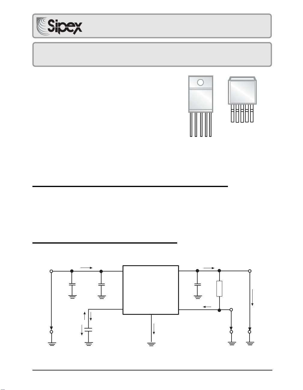
Sipex’s SPX2975 is a low dropout linear regulator with integrated PNP pass transistor. The part
is available in a 5 pin TO-220 package or surface mount TO-263. The part used to convert an
automotive battery voltage, with allowable input up to 45V, down to 5V with at least 400mA output
current delivered. Internal power consumption is kept to 60uA ideal for applications where micropower operation is important. At over-temperature the SPX2975 is turned off by the integrated
temperature protection circuit. A reset signal is generated for a typical output voltage of 4.65V
with a time delay that can be programmed by an external delay capacitor.
TYPICAL APLICATION CIRCUIT
SPX2975
5 Pin TO-263
12345
I
RD
OUT
RO
V
GND
DESCRIPTION
I
C
Q
22µF
OUT
I
RO
R
5kΩ
EXT
V
RD
I
IN
C
11
1000µF
V
IN
RD,d
I
RD,c
C
D
47nF
I
V
Date: 1/17/05 SPX2975 400mA Low Dropout Voltage Regulator © Copyright 2005 Sipex Corporation
RD
C
12
100nF
RD
I
1
SPX2975
4
3
GND
I
GND
V
OUT
5
RO
2
1
V
OUT
Page 2
Input Voltage ...................................................................... -42V to 45V
Output Voltage .................................................................... -1.0 to 16V
Output Current ............................................................ Internally limited
Reset Output Voltage .......................................................... -0.3 to 25V
Reset Output Current ..................................................... -5mA to +5mA
Reset Delay Voltage ........................................................ -0.3V to 7.0V
Reset Delay Current ......................................................... -2mA to 2mA
Storage Temperature .................................................. -50°C to +150°C
Junction Temperature.(Note 1) ................................... -40°C to +150°C
(TO-252)............................................................................... 78°C/W
T
JA
T
(TO-220)............................................................................... 65°C/W
JA
T
(TO-263)............................................................................... 53°C/W
JA
(TO-220, T0 263, and TO-252).............................................. 4°C/W
T
JC
These are stress ratings only and functional operation of the device at
these ratings or any other above those indicated in the operation sections
of the specifications below is not implied. Exposure to absolute maximum
rating conditions for extended periods of time may affect reliability.
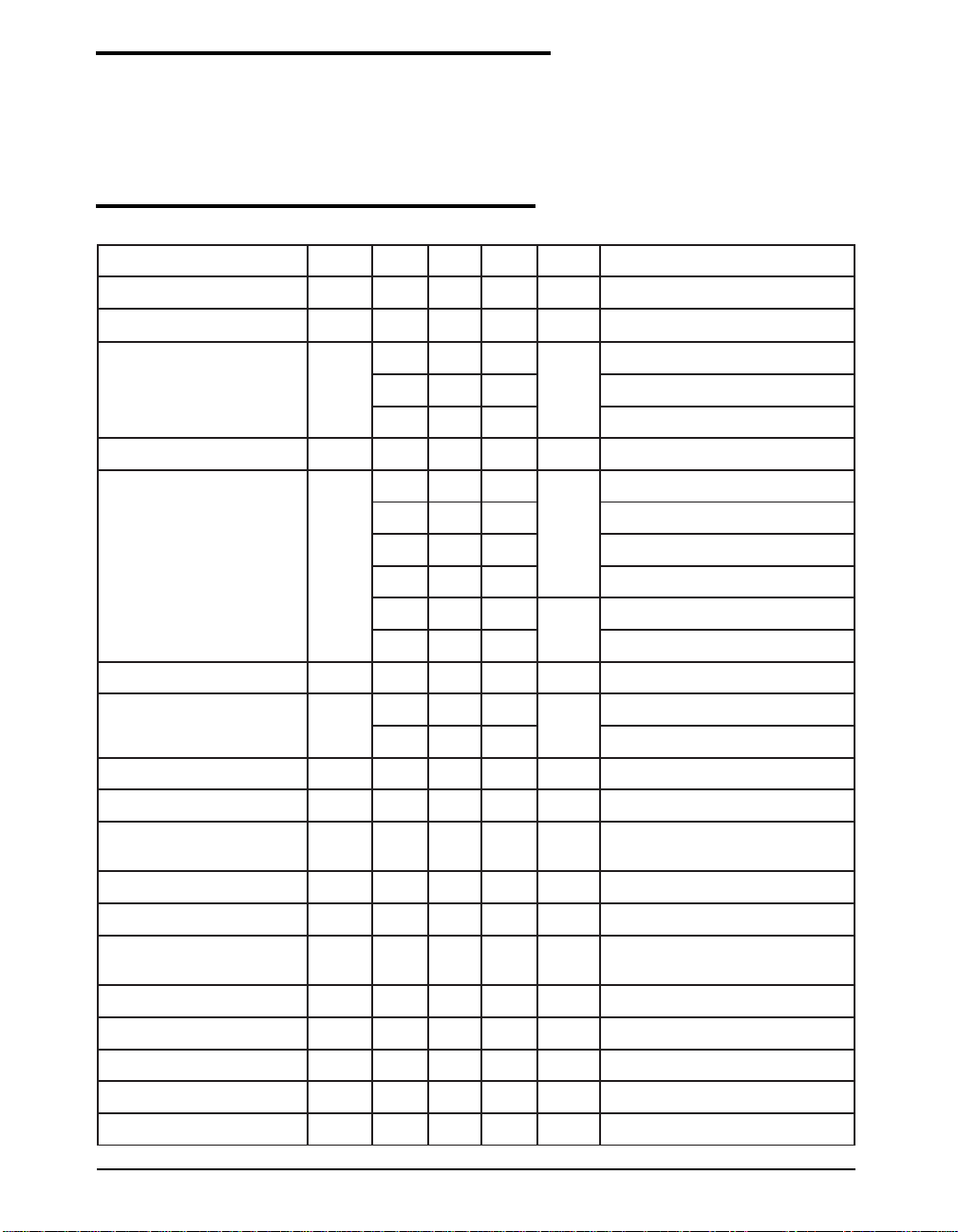
ELECTRICAL CHARACTERISTICS
ABSOLUTE MAXIMUM RATINGS
VIN = 13.5V; -40°C < Tj < 150°C. Unless otherwise specified.
RETEMARAPMYS.NIM.PYT.XAMSTINUSNOITIDNOC
egatloVtupnIV
erutarepmeTnoitcnuJT
egatloVtuptuOV
noitatimiltnerruCtuptuOI
noitpmusnoCtnerruCI
I
J
Q
Q
q
)1eton(egatloVtuoporDV
noitalugeRdaoL
noitalugeReniL
∆V
∆V
RRSP
egatloVtuptuOerutarepmeT
Vd
tfirD
Q
dlohserhTgnihctiwSteseRV
egatloVwoLtuptuOteseRV
tnerruC
egakaeLtuptuOteseR
tnerruCgnigrahCteseRI
dlohserhTgnimiTreppUV
I
D
UD
dlohserhTgnimiTrewoLV
emiTyaleDteseRt
emiTnoitcaeRteseRt
Note 1: Measured when the output voltage (Vout) has dropped 100mV form the nominal value obtained at Vin=13.5V
Date: 1/17/05 SPX2975 400mA Low Dropout Voltage Regulator © Copyright 2005 Sipex Corporation
d
RR
5.524V
04-051
9.40.51.5
9.40.51.5I<Am5
9.452.5I≤Aµ001
054007Am
06001
06021I
07081I
07002I
701
7122I
rd
053005VmI
03-503
Q
Q
RRSP
002-002I
51-251VmV
06BdfrV;zH001=
Td/2.0K/Vm
TR
LQR
HQR
15.456.48.4VV
2.04.0VR
001Aµ
0.35.50.9AµVDRV1=
5.18.12.2VhtV
2.04.07.0VhtV
LD
016122smC
5.00.2sµC
ºC
I<Am5
Q
V
Aµ
Am
Vm
Q
Q
I
TUO
TUO
TUO
TUO
I
TUO
TUO
TUO
I
TUO
TUO
NI
HT
txe
V
HOR
H
L
O
O
001=µT,A
V5=
T,Aµ001=
j
j
T,Am1=
j
T,Am1=
j
Am052=
Am004=
V,Am003=
OD
I≤Aµ001=
Q
I,V23otV8=
r
V;Ωk5≥
dT,Fn74=
vrT,Fn74=
52= ºC
58= ºC
TUO
52= ºC
58= ºC
Am004otAm5=
TUO
V<V6,Am004<
V82<
I
V<V6,Am002<
V04<
I
V<V6,Am5≤
V82<
I
V=
TUO-VNI
Am5≤
Am5=
ppV5.0=
V1>
2
Page 3
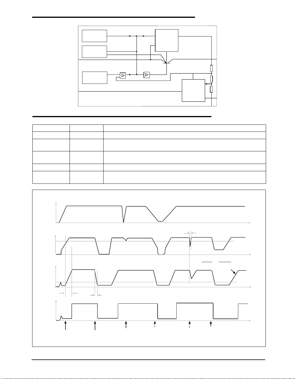
FUNCTIONAL DIAGRAM
V
RD
IN
Temperature
Sensor
Current
Limit
1
Bandgap
Reference
4
Buffer
Saturation
Control &
Protection
Circuit
Reset
Generator
3
GND
5
V
OUT
2
RO
PIN DESCRIPTION
PIN NUMBER PIN NAME DESCRIPTION
1V
IN
2ROReset Output. RO remains low while V
3 GND Ground. This pin also functions as a heatsink. Solder to large pads or the
4RDReset Delay. RD connects capacitor to GND for setting delay time.
5V
V
I
OUT
LDO Input. Bypass VIN to GND with a Ceramic capacitor.
is below the reset switching
threshold. RO is in open conector output.
OUT
circuit-board ground plane to maximize thermal dissipation.
LDO Output. Bypass V
ESR less than 5Ω at 10kHz.
to GND with a minimum 22µF capacitor with
OUT
V
Q, rt
V
DU
V
DRL
t
t
t
V
Q
V
D
t
RO
rd
V
t
RR
<t
rr
dV
I
D
=
C
dt
D
t
Power on
Reset
Thermal
Shutdown
Voltage Dip
at Input
Undervoltage
Secondary
Spike
Overload
at Output
Reset Timing
Date: 1/17/05 SPX2975 400mA Low Dropout Voltage Regulator © Copyright 2005 Sipex Corporation
3
Page 4
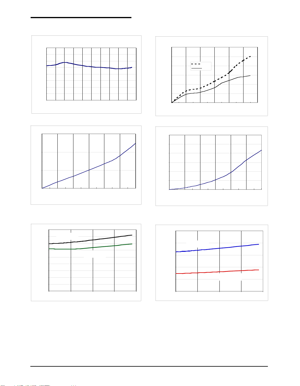
TPYICAL PERFORMANCE CHARACTERISTICS
I
Output Current Limit Vs Temperature
800
700
600
500
400
(mA)
OUT
I
300
200
100
0
-40 -20 0 20 40 60 80 100 120 140 160
Current Consumption Iq vs Output Current IQ
Temperature (ºC)
3
2
(mA)
Q
I
1
0
020406080100 120
Output Current IQ (mA)
Dropout Voltage Vdr Vs Output Current I
1200
1000
800
600
400
Dropout Voltage Vdr (mV)
200
0
0 100 200 300 400 500 600
60
Current Consumption Iq vs Output Current I
125C
25C
Output Current IQ
Q
Q
50
40
30
(mA)
Q
I
20
10
0
0 100 200 300 400 500 600
Output Current I
(mA)
Q
9E-05
8E-05
7E-05
6E-05
5E-05
Iq (A)
4E-05
3E-05
2E-05
1E-05
0E+00
-40 10 60 110 160
Iq vs Temperature
Iload = 1mA
Iload = 100uA
Temperature (°C)
2.5E-02
2.0E-02
1.5E-02
Iq (A)
1.0E-02
5.0E-03
0.0E+00
-40 10 60 110 160
Iq vs Temperature
load = 400mA
Iload = 250mA
Temperature (°C)
Date: 1/17/05 SPX2975 400mA Low Dropout Voltage Regulator © Copyright 2005 Sipex Corporation
4
Page 5
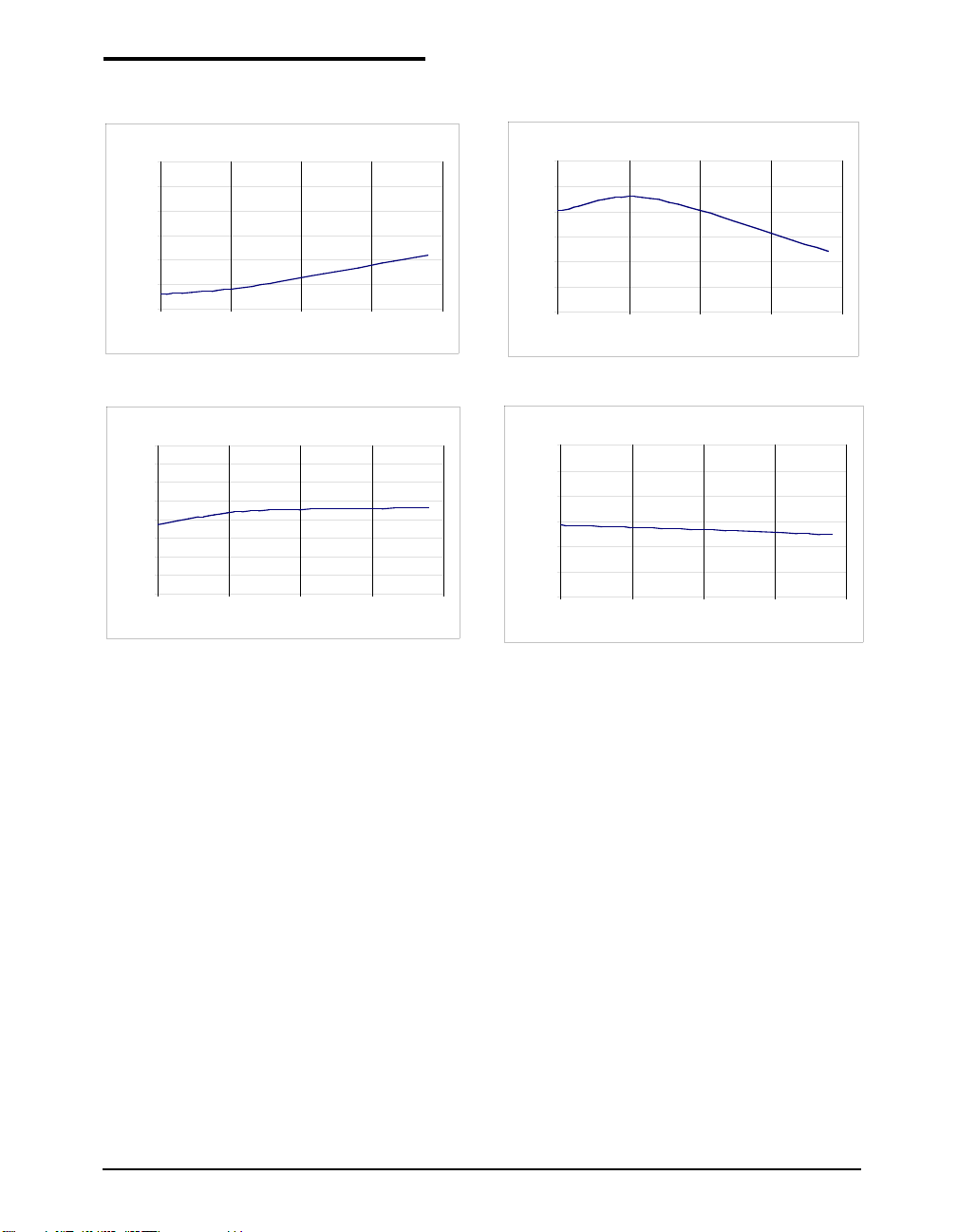
TPYICAL PERFORMANCE CHARACTERISTICS
Load Regulation vs Temperature
0.030
0.025
0.020
0.015
0.010
Load Regulation (V)
0.005
0.000
-40 10 60 110 160
5.20
5.15
5.10
5.05
5.00
@ 42V (V)
4.95
OUT
V
4.90
4.85
4.80
-40 10 60 110 160
Temperature (°C)
V
vs Temperature
OUT
Temperature (°C)
Reset Threshold vs Temperature
4.8
4.75
4.7
4.65
4.6
Reset Threshold (V)
4.55
4.5
-40 10 60 110 160
0.022
0.020
0.018
0.016
0.014
0.012
Reset Delay Time (sec)
0.010
-40 10 60 110 160
Temperature (°C)
Reset Delay vs Temperature
Temperature (°C)
Date: 1/17/05 SPX2975 400mA Low Dropout Voltage Regulator © Copyright 2005 Sipex Corporation
5
Page 6
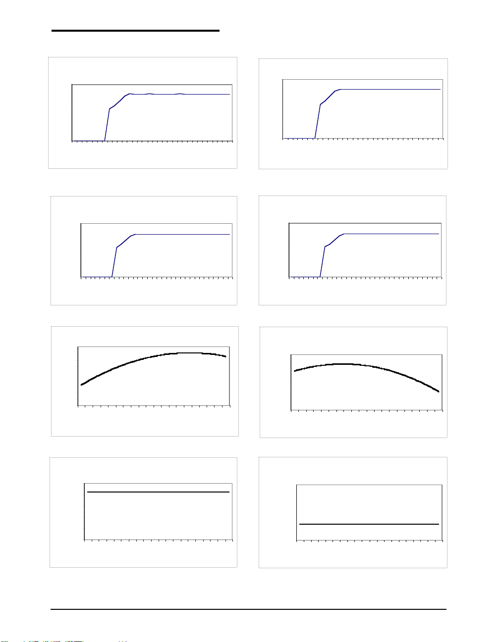
TPYICAL PERFORMANCE CHARACTERISTICS
VIN vs. V
, RL= 25Ω, Temp = 125ºC
OUT
6
5
4
(V)
3
OUT
V
2
1
0
0 2.5 5 10 203040
Vin ( V )
I
vs. VIN, Temp = 125ºC, Rl = 25Ω
OUT
250
200
150
(mA)
100
OUT
I
50
0
0 2.5 5 10 203040
V
(V)
IN
V
Vs Temp, VIN = 13.5 V
OUT
(V)
OUT
V
5.02
5.01
4.99
4.98
4.97
4.96
4.95
4.94
4.93
5
-40 -20 0 20 40 60 80 100 120 140
Temp (ºC)
VIN vs. V
, RL = 25Ω, temp = 25ºC
OUT
6
5
4
(V)
3
OUT
V
2
1
0
02.5 5 10203040
Vin (V)
I
Vs VIN, Temp = 25ºC, RL = 25Ω
OUT
250
200
150
(mA)
100
OUT
I
50
0
0 2.5 5 10 203040
V
(V)
IN
Chrage I Vs Temp, VIN = 13.5V, VD = 1V
5.75
5.7
5.65
5.6
5.55
Charge I (uA)
5.5
5.45
-40 -20 0 20 40 60 80 100 120 140
Temp (ºC)
V
Lower Threshold vs. Temp, VIN = 13.5V
D
0.5
0.4
0.3
(V)
0.2
lower Threshold
D
0.1
V
0
-40 -20 0 20 40 60 80 100 120 140
Temp (deg C)
Date: 1/17/05 SPX2975 400mA Low Dropout Voltage Regulator © Copyright 2005 Sipex Corporation
V
upper Threshold vs. Temp, V
D
1.86
1.86
1.86
1.86
( V)
1.86
1.86
1.86
Vd Upper Threshold
1.86
-40 -20 0 20 40 60 80 100 120 140
Temp (ºC)
= 13.5V
IN
6
Page 7
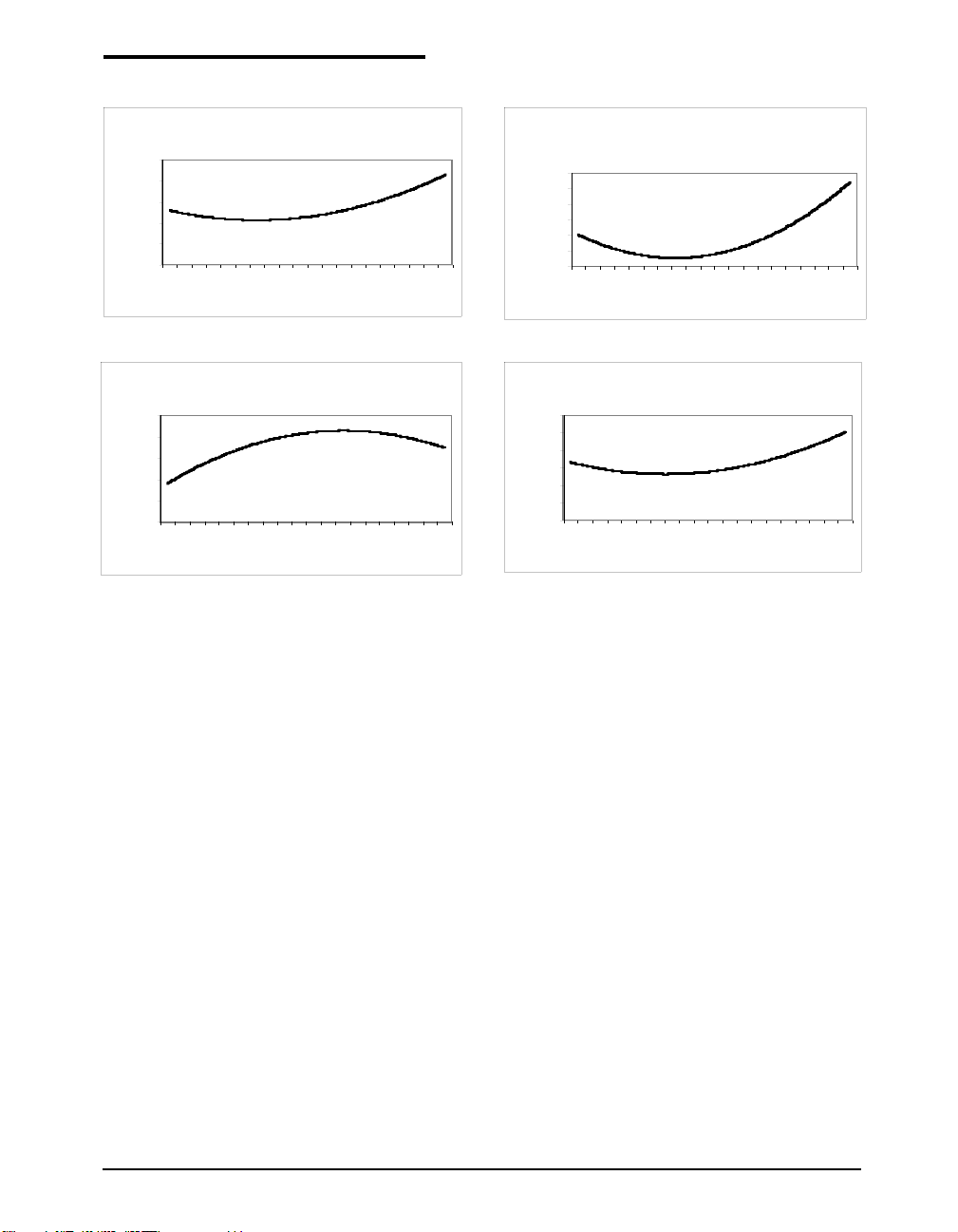
TPYICAL PERFORMANCE CHARACTERISTICS
I_limit vs. Temp, V
0.9
0.85
0.8
0.75
I limit ( mA)
0.7
0.65
-40 -20 0 20 40 60 80 100 120 140
Reset Threshold vs. Temp, V
4.62
4.6
4.58
4.56
4.54
Reset Threshold (V)
4.52
-40 -20 0 20 40 60 80 100 120 140
IN
Temp (ºC)
Temp (ºC)
= 13.5V
IN
= 13.5V
Load Regulation vs. Temp
V
=13.5 V, I
IN
0.012
0.01
0.008
0.006
0.004
Load reg (V)
0.002
0
-40 -20 0 20 40 60 80 100 120 140
= 100µA and 400mA
Q
Temp (ºC)
Reset Delay vs. Temp, VIN = 13.5V
16
15.8
15.6
15.4
15.2
15
Reset Delay (msec)
14.8
-40 -20 0 20 40 60 80 100 120 140
Temp (ºC)
Date: 1/17/05 SPX2975 400mA Low Dropout Voltage Regulator © Copyright 2005 Sipex Corporation
7
Page 8
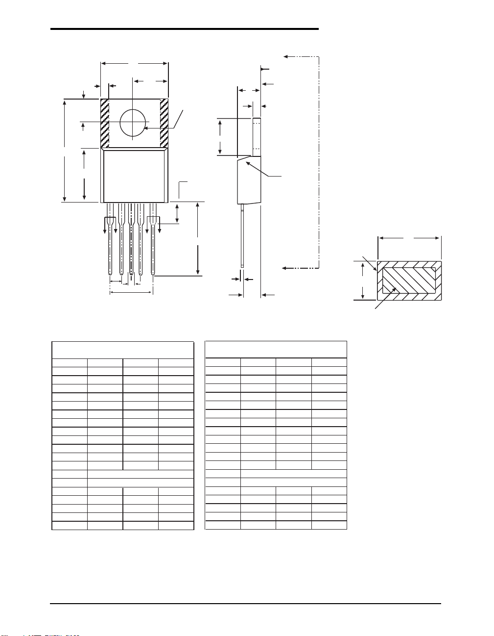
PACKAGE: 5 PIN TO-220
E
E2
Q
D
D1
1
C
C
e
E/2
e
DD
b
e1
5 Pin TO-220 JEDEC TO-220 (AC)
Variation
SYMBOL
MIN NOM MAX
A 0.16 - 0.19
A1 0.02 - 0.055
A2 0.08 - 0.115
b 0.015 0.027 0.04
b2 0.045 - 0.07
c 0.014 - 0.024
D 0.56 - 0.65
D1 0.33 - 0.355
D2 0.48 - 0.507
E 0.38 - 0.42
E1 0.27 - 0.35
E2 - - 0.03
e
e1
.100 BSC
.100 BSC
H1 0.23 - 0.27
L1 - - 0.25
L2 --∆P 0.139 - 0.161
Q 0.1 - 0.135
Note: Dimensions in (mm)
øP
H1
L1
L
C
5 Pin TO-220 JEDEC TO-220 (AC)
SYMBOL
A 0.006 - 0.007
A1 0.001 - 0.002
A2 0.003 - 0.005
b 0.001 0.001 0.002
b2 0.002 - 0.003
c 0.001 - 0.001
D 0.022 - 0.026
D1 0.013 - 0.014
D2 0.019 - 0.020
E 0.015 - 0.017
E1 0.011 - 0.014
E2 - - 0.001
e
e1
H1 0.009 - 0.011
L1 - - 0.010
L2 --∆P 0.005 - 0.006
Q 0.004 - 0.005
Note: Dimensions in (inch)
A
B
SEATING
PLANE
A
A1
CHAMFER
OPTIONAL
A
A2
Variation
MIN NOM MAX
.004 BSC
.004 BSC
b
WITH PLATING
c
BASE METAL
CONTACT AREA
Date: 1/17/05 SPX2975 400mA Low Dropout Voltage Regulator © Copyright 2005 Sipex Corporation
8
Page 9
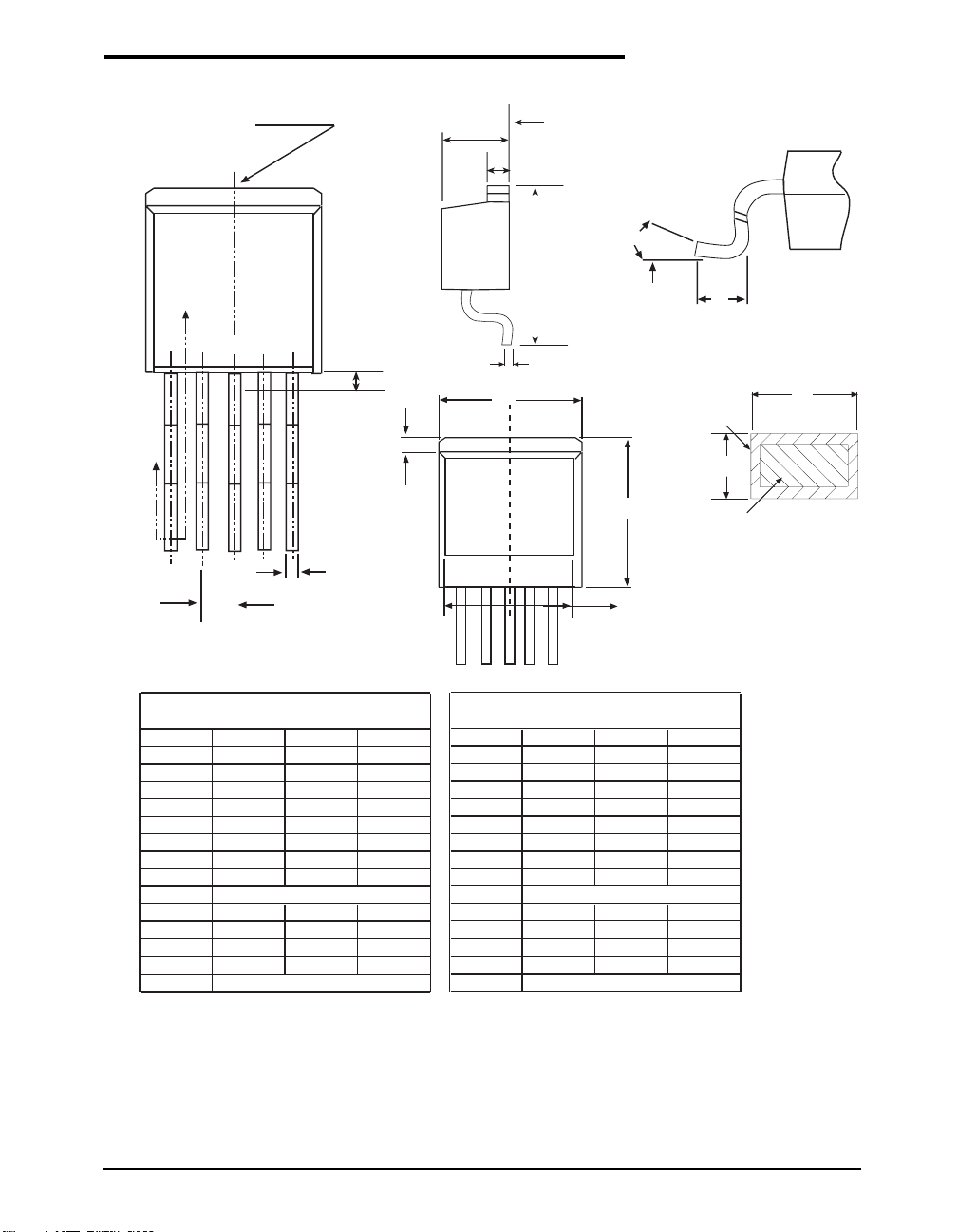
PACKAGE: 5 PIN TO-263
4X
(DATUM A)
E
1
23
E
e
SEATING PLANE
A
C2
0º-8º
H
L3
5
4
c
L2
(E)
L1
WITH PLATING
D1
L
(b)
c
BASE METAL
CONTACT AREA
5X b
E1
5 Pin TO-263 JEDEC TO-263 (BB)
SYMBOL
A 0.16 - 0.19
A1 0 - 0.01
b 0.02 - 0.039
c 0.015 - 0.029
c2 0.45 - 0.23
D1 0.27 - -
E 0.38 - 0.42
E1 0.245 - -
e
H 0.575 - 0.625
L 0.07 - 0.11
L1 - - 0.066
L2 - - 0.07
L3
Note: Dimensions in (mm)
Date: 1/17/05 SPX2975 400mA Low Dropout Voltage Regulator © Copyright 2005 Sipex Corporation
Variation
MIN NOM MAX
.067 BSC
.010 BSC
5 Pin TO-263 JEDEC TO-263 (BB)
SYMBOL
A 0.006 - 0.007
A1 0.000 - 0.000
b 0.001 - 0.002
c 0.001 - 0.001
c2 0.018 - 0.009
D1 0.011 - -
E 0.015 - 0.017
E1 0.010 - -
e
H 0.023 - 0.025
L 0.003 - 0.004
L1 - - 0.003
L2 - - 0.003
L3
Note: Dimensions in (inch)
Variation
MIN NOM MAX
.026 BSC
.004 BSC
9
Page 10
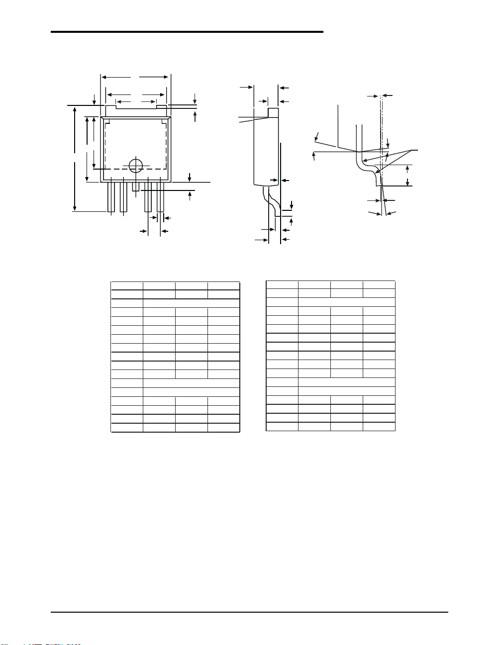
PACKAGE: 5 PIN TO-252
E
b3
b4
L3
D1
D
H
b
e
L2
7º
L4
A
c2
GAUGE PLANE
7º
RO.012
7º
A1
L1
0.002 min
L
c
c3
4º±4º
Symbol MIN NOM MAX
A 0.086 0.090 0.094
b
0.020 TYP
b3 0.205 0.210 0.215
b4 - 0.110 -
c 0.020 0.021 0.022
c2 0.018 0.020 0.022
c3 0.037 0.040 0.043
D 0.235 0.240 0.245
D1 0.184 0.189 0.194
E 0.253 0.258 0.263
e 0.045 TYP
H 0.390 TYP
L1 0.051 0.053 0.055
L2 - 0.013 L3 0.037 0.042 0.047
L4 0.028 0.032 0.036
Note: dimensions in (INCHES)
Symbol MIN NOM MAX
A 2.18 2.29 2.39
b
0.51 TYP
b3 5.21 5.33 5.46
b4 - 2.79 -
c 0.51 0.53 0.56
c2 0.46 0.51 0.56
c3 0.94 1.02 1.09
D 5.97 6.10 6.22
D1 4.67 4.80 4.93
E 6.43 6.55 6.68
e
1.14 TYP
H 9.91 TYP
L1 1.30 1.35 1.40
L2 - 0.33 L3 0.94 1.07 1.19
L4 0.71 0.81 0.91
Note: Dimensions in (mm)
Http://www.omedata.com
Date: 1/17/05 SPX2975 400mA Low Dropout Voltage Regulator © Copyright 2005 Sipex Corporation
10
Page 11
ORDERING INFORMATION
Part number Accuracy Output Voltage Package Type
SPX2975R5-5.0 ................. .........2% ......................... 5.0V .....................5 Lead TO-252
SPX2975R5-5.0/TR ........... .........2% ......................... 5.0V .....................5 Lead TO-252
SPX2975T5-5.0 ................. .........2% ......................... 5.0V .....................5 Lead TO-263
SPX2975T5-5.0/TR ........... .........2% ......................... 5.0V ..................... 5 Lead TO-263
SPX2975U5-5.0 ................. .........2% ......................... 5.0V ..................... 5 Lead TO-220
Available in lead free packaging. To order add "-L" suffix to part number.
Example: SPX2975T5-5.0/TR = standard; SPX2975T5-5.0-L/TR = lead free
/TR = Tape and Reel
Pack quantity is 500 for TO-263 and 2,000 for TO-252.
CLICK HERE TO ORDER SAMPLES
Corporation
ANALOG EXCELLENCE
Sipex Corporation
Headquarters and
Sales Office
233 South Hillview Drive
Milpitas, CA 95035
TEL: (408) 934-7500
FAX: (408) 935-7600
Sipex Corporation reserves the right to make changes to any products described herein. Sipex does not assume any liability arising out of the
application or use of any product or circuit described herein; neither does it convey any license under its patent rights nor the rights of others.
Date: 1/17/05 SPX2975 400mA Low Dropout Voltage Regulator © Copyright 2005 Sipex Corporation
11
 Loading...