

Page 1
123
SPX1582
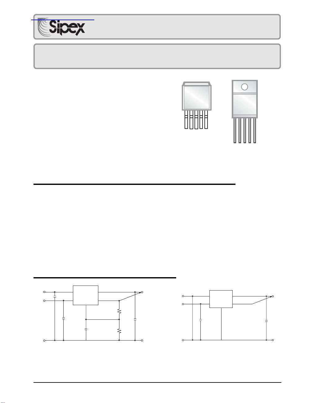
5 Pin TO-263
SENSE
ADJ OR FIXED
V
OUT
V
CNTRL
V
IN
查询SPX1582供应商
®
SPX1582
3A Ultra Low Dropout Voltage Regulator
Fast Response, Adjustable & Fixed
FEATURES
■Low Dropout Voltage 500mV at 3A Full Load Current
■Adjustable Ouput Down to 1.25V from ATX Power Supply
■Fixed Output Voltages of 3.3V and 2.5V
■Extremely Tight Load and Line Regulation
■Standard 5-Terminal Low Cost TO-220 and TO-263
APPLICATIONS
■3.3V to 2.8V ATX Power Supplies
■3.3V to 2.9V for Portable PENTIUMTM Processor
■5V to 3.5V VRE Supply
■High efficiency "Green" Computer Systems
The SPX1582 is a 3A Low Dropout Regulator with extremely low dropout voltage. The adjustable version requires only
two external resistors to set the output voltage. The fixed version has a preset output of 3.3V, 2.8V or 2.5V and does
not require any external resistors. The SPX1582 features a low dropout of 400mV(Typ.) and offers fast transient
response. This device is suitable for Pentium applications requiring 2.8V, 2.5V from 3.3V ATX power supplies, where
a low current input voltage 1V greater than the output voltage is needed. With an external sense pin the load regulation
is less than 1mV. This device is an excellent choice for the use of powering low voltage microprocessors that require
a lower dropout, fast transient response to regulate from 3.3V and 5V supplies. The SPX1582 is also an excellent choice
as a post regulator for switching supplies applications.
The SPX1582 offers protection against over-current faults, reversed input polarity, over temperature operation and
positive and negative transient voltage.
The SPX1582 is offered in a 5 pin TO-220 and TO-263 compatible with industry standard 5-terminal regulators. For 5A,
3A and 1.5A ultra low dropout versions refer to SPX1581, SPX1582 and SPX1583 data sheets respectively.
Now Available in Lead Free Packaging
SPX1582
5 Pin TO-220
4
5
321
IN
V
OUT
V
CNTRL
V
SENSE
ADJ OR FIXED
DESCRIPTION
Adjustable Regulator
TYPICAL APPLICATIONS CIRCUIT
V
3.3V
V
5V
V
IN
CTRL
C1
330µF
IN
5
SPX1582
4
CTRL
C2
10µF
(1) V
(2) V
(3) V
2
CTRL
OUT
REF
V
Date:5/25/04 SPX1582 3A Ultra Low Dropout Voltage Regulator ©Copyright 2004 Sipex Corporation
V
OUT
3
1
SENSE
ADJ
C3
.033µF
needed when V
= V
(1+R2/R1)+I
REF
is measured across adjust to sense.
R1
124Ω
R2
124Ω
< 5V.
IN
.
ADJ R2
2.5V
V
OUT
C4
2x330µF
V
3.3V
V
5V
V
IN
CTRL
C1
330µF
IN
5
4
V
CTRL
C2
10µF
Typical Fixed Regulator
SPX1582
2
(1) V
CTRL
V
3
1
GND
needed when V
OUT
SENSE
2.5V
V
C4
2x330µF
< 5V.
IN
1
OUT
Page 2
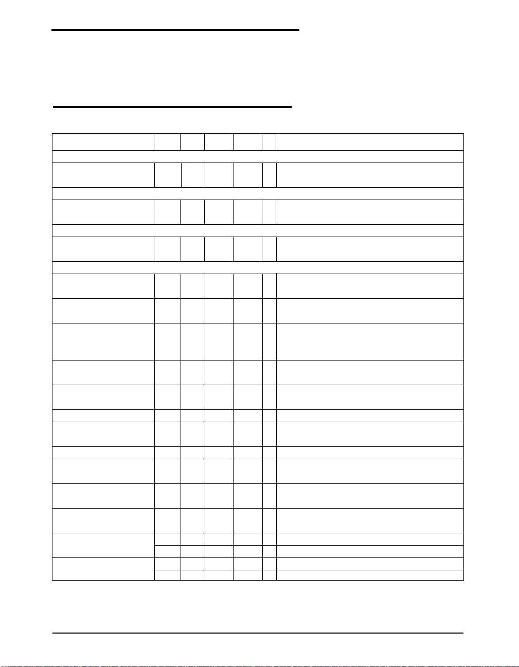
ABSOLUTE MAXIMUM RATINGS
Power Dissipation ..................................... Internally Limited
Lead Temp. (Soldering, 10 Seconds)......................... 300°C
Storage Temperature Range ..................... -65°C to +150°C
Operating Junction Temperature Range
SPX1582 Control Section ............................. 0°C to +125°C
SPX1582 Power Transistor .......................... 0°C to +150°C
Input Supply Voltage ..................................................... 6V
Input Voltage ....................................................... 13V
V
CTRL
ELECTRICAL CHARACTERISTICS
Electrical characteristics at V
The ♦ denotes the specifications which apply over full temperature range -40°C to +85°C, unless otherwise specified.
PARAMETER MIN TYP MAX UNITS CONDITIONS
2.5V Version
Output Voltage 2.450 2.5 2.550 V V
2.8V Version
Output Voltage 2.744 2.8 2.856 V V
3.3V Version
Output Voltage 3.234 3.3 3.366 V V
All Voltage Options
Reference Voltage 1.238 1.25 1.263 V V
Line Regulation mV V
Load Regulation (Note 1) 1.0 5.0 mV
0V
= V
SENSE
, V
OUT
2.400 2.600
2.688 2.912
3.168 3.3 3.432
1.0 3.0
= 0V, TA=25°C, C
ADJ
= C
CTL
PWR
= 6.0V to 12V, VIN = 3.0V to 5.0V, IO =10mA
CTRL
♦
IO = 10mA to 3A
= 6.3V to 12V, VIN =3.3V + 0.8V, IO=10mA
CTRL
♦
IO = 10mA to 3A
= 6.3V to 12V, VIN = 3.3V + 0.8V, IO=10mA
CTRL
♦
IO = 10mA to 3A
= 2.75V, VIN = 2.00V, IO = 10mA
CTRL
V
=2.7V to 12V,VIN = 2.05V to 5.5V,IO=10mA to 7A
CTRL
= 2.5V to 12V, V
CTRL
♦ V
= 0V
ADJ
♦
V
= 2.75V, V
CTRL
= C
= 33µF tantalum cap otherwise specified.
OUT
= 1.75 to 5.5V, IO=10mA
IN
= V
IN
1.5V, IO=10mA to 3A, V
OUT +
ADJ
=
Dropout Voltage Min. V
(Note 2) (VIN - V
Dropout Voltage Min. V
(Note 2) (VIN - V
CTRL
)V
OUT
IN
)V
OUT
Current Limit 3.1 A V
Minimum Load Current 5 10 mA
1.05 1.18 V V
0.40 0.50 V V
♦
= 0V
ADJ
= 2.05V, IO = 1A
IN
= 0V
ADJ
= 2.75V, IO = 3A
IN
= 2.75V, V
CTRL
V
= 5V, VIN=3.3V, V
CTRL
= 2.05V, ∆ V
IN
ADJ
=0V
= 100mV, V
OUT
ADJ
= 0V
Thermal Regulation 0.002 0.02 %/W 30ms Pulse
Ripple Rejection 60 80 dB V
Control Pin Current 60 120 mA
♦
Adjustble Pin Current 50 µAV
120
♦
= 3.75V, V
CTRL
TJ=25, V
V
= 0V
ADJ
V
= 2.75V, V
CTRL
= 2.75V, V
CTRL
= 3.75V, IO = 2.3A, V
IN
=1Vpp at 120Hz
RIPPLE
= 2.05V, IO = 3A
IN
= 2.05V, V
IN
ADJ
=0V, IO = 10mA
ADJ
=0V
Thermal Resistance 3 °C/W Junction to Case (θJC)
TO-220-5 50 °C/W Junction to Ambient (θJA)
Thermal Resistance 3 °C/W Junction to Case (θJC)
TO-263-5 60 °C/W Junction to Ambient (θJA)
Note 1: Low duty cycle pulse testing with Kelvin connections is required to order to maintain accurate data.
Note 2: Dropout voltage is defined as the minimum differential between VIN and V
maintain regulation at V
Note 3: V
Date:5/25/04 SPX1582 3A Ultra Low Dropout Voltage Regulator ©Copyright 2004 Sipex Corporation
is measured across Adjust pin to Sense pin.
REF
95% Nominal V
OUT
OUT
.
OUT
or V
CTRL
and V
required to
OUT
2
Page 3
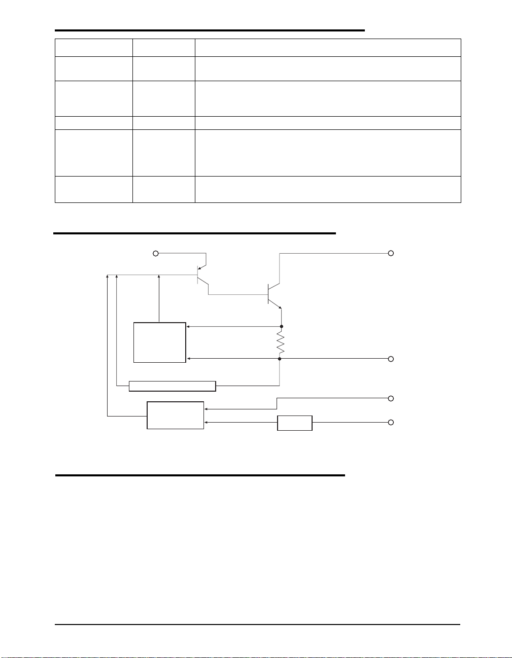
PIN DESCRIPTION
PIN NUMBER PIN NAME DESCRIPTION
1 SENSE Allows Kelvin sense of V
at the load. (Positive side of the
OUT
reference voltage of the device).
2 ADJ Negative side of the reference voltage for the device. Adding a small
bypass capacitor from the ADJ pin to ground will improve the transient
response.
3V
4V
OUT
CTRL
Power output of the device.
Supply pin for the control circuitry of the device. The current flow into this
pin will be about 1% of the output current. V
must be between 1.0V
CTRL
and 1.3V greater than the output voltage for the
device to regulate.
5V
IN
Output load current is supplied through this pin. V
must be between 0.1V
IN
and 0.8V greater than the output voltage for this device to regulate.
FUNCTIONAL DIAGRAM
(4) V
CTRL
CURRENT
LIMIT
AMPLIFIER
THERMAL OVERLOAD
VOLTAGE
REGULATION
AMPLIFIER
LIMIT
SENSE
The SPX1582 is designed as a high performance
and low cost solution for application requiring a
lower dropout than traditional NPN regulators.
The SPX1582 uses a separate input voltage V
( V
CTRL
≥ V
+ 1.3V) to minimize the dropout
OUT
CTRL
voltage. This allows the 2.5V power for the load
to come from a 3.3V system supply.
As added benefit this will reduce the heat dissipation*, and lower heatsink and cooling fan cost.
V
(5)
IN
(3)
V
OUT
SENSE (1)
V
REF
ADJ (2)
APPLICATION NOTES
A typical application would use 3.3V for V
and 5.0V for V
from a motherboard power
CTRL
supply to provide a nominal 2.5V output. Using
the sense pin allows Kelvin measure the output,
reducing resistance-associated errors.
The SPX1582 can power the 2.5V core voltage
for microprocessors such as a PentiumPCTM,
P55CTM, AMD5k86TM and K6TM and the IBM
PowerPCTM 603EV and 604EV processors.
IN
Date:5/25/04 SPX1582 3A Ultra Low Dropout Voltage Regulator ©Copyright 2004 Sipex Corporation
3
Page 4

Adjustable Regulator Design
1.25V reference voltage is being developed between the SENSE pin and the ADJ pin of the
SPX1582. Adding two external resistors (see fig
1.) will allow setting the output voltage from
1.25V to 6V. R
specified minimum load current of 10mA. R
given by the formula: V
+ I
(R2). The current flowing from the ADJ
ADJ
is chosen so that this current is
1
OUT
= V
(1+ R2/R1)
REF
is
2
pin is typicaly 50µA. This ADJ pin contributes
to the final V
but is usually neglected.
OUT
Connecting the sense pin to the top of the resistor divider will improve load regualtion.
Lowering Noise
Using the SENSE pin to Kelvin the load will
increase accuracy of the output voltage during
load regulation. For the fixed voltage device,
adding a capacitor at the GND pin will improve
transient response. THis capacitor is chosen in
the range of 1µF to 0.1µF and will depend on the
amount of output capacitance in the system.
APPLICATION NOTES: Continued
Date:5/25/04 SPX1582 3A Ultra Low Dropout Voltage Regulator ©Copyright 2004 Sipex Corporation
4
Page 5
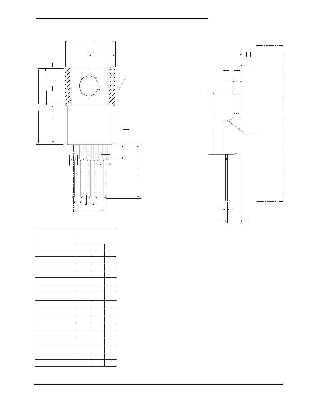
PACKAGE: 5 Pin TO-220
H1
E
E/2
Q
øP
A
B
F
A
SEATING
PLANE
D
D1
L1
D
C
C
e
D
L
b
e1
D
CHAMFER
OPTIONAL
A
C1
J1
5 PIN TO-220
A
b
C1
D
E
e
e1
F
H1
J1
L
L1
∆P
Q
U
V
Date:5/25/04 SPX1582 3A Ultra Low Dropout Voltage Regulator ©Copyright 2004 Sipex Corporation
Dimensions in
(inches)
MIN NOM MAX
.160 - .190
.015 - .040
.014 - .022
.560 - .590
.385 - .415
.385 - .415
.062 - .072
.045 - .055
.234 - .258
.090 - .115
.540 - .560
- .250
.146 - .156
.103 - .113
- .30 -
- .24 -
5 PIN TO-220
5
Page 6
4X
(DATUM A)
E
1
23
E
e
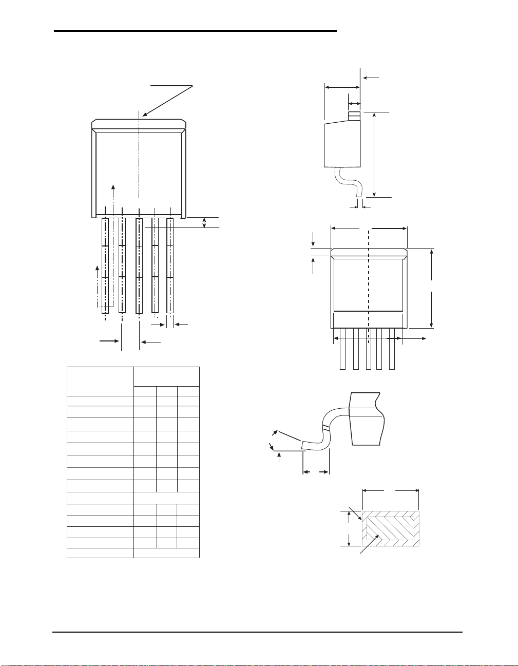
PACKAGE: 5 Pin TO-263
SEATING PLANE
A
C2
H
5
4
L2
L1
5X b
c
(E)
D1
E1
5 PIN TO-263
JEDEC TO-263
(BB) Variation
A
A1
b
c
c2
D1 .270 - -
E
E1
e .067 BSC
H
L
L1
L2
L3
Dimensions in (mm)
MIN NOM MAX
.160 - .190
0 - .010
.020 - .039
.015 - .029
.045 - .023
.380 - .420
.245
-
.575 - .625
.070 - .110
-
-
- .010 BSC
.066
.070
0º-8º
L3
-
L
(b)
WITH PLATING
c
BASE METAL
CONTACT AREA
5 PIN TO-263
Date:5/25/04 SPX1582 3A Ultra Low Dropout Voltage Regulator ©Copyright 2004 Sipex Corporation
6
Page 7
ORDERING INFORMATION
Part Number Accuracy Output Voltage Packages
SPX1582U5 ............................... 2.0%............................. Adj.......................... 5-Pin TO-220
SPX1582U5-2.5 ......................... 2.0%............................ 2.5V ........................ 5-Pin TO-220
SPX1582U5-2.8 ......................... 2.0%............................ 2.8V ........................ 5-Pin TO-220
SPX1582U5-3.3 ......................... 2.0%............................ 3.3V ........................ 5-Pin TO-220
SPX1582T5................................ 2.0%............................. Adj.......................... 5-Pin TO-263
SPX1582T5/TR .......................... 2.0%............................. Adj.......................... 5-Pin TO-263
SPX1582T5-2.5.......................... 2.0%............................ 2.5V ........................ 5-Pin TO-263
SPX1582T5-2.5/TR.................... 2.0%............................ 2.5V ........................ 5-Pin TO-263
SPX1582T5-2.8.......................... 2.0%............................ 2.8V ........................ 5-Pin TO-263
SPX1582T5-2.8/TR.................... 2.0%............................ 2.8V ........................ 5-Pin TO-263
SPX1582T5-3.3.......................... 2.0%............................ 3.3V ........................ 5-Pin TO-263
SPX1582T5-3.3/TR.................... 2.0%............................ 3.3V ........................ 5-Pin TO-263
Available in lead free packaging. To order add "-L" suffix to part number.
Example: SPX1582T5-3.3/TR = standard; SPX1582T5-L-3.3/TR = lead free
/TR = Tape and Reel
Pack quantity is 500 for TO-263.
Corporation
ANALOG EXCELLENCE
Sipex Corporation
Headquarters and
Sales Office
233 South Hillview Drive
Milpitas, CA 95035
TEL: (408) 934-7500
FAX: (408) 935-7600
Sales Office
22 Linnell Circle
Billerica, MA 01821
TEL: (978) 667-8700
FAX: (978) 670-9001
e-mail: [email protected]
Sipex Corporation reserves the right to make changes to any products described herein. Sipex does not assume any liability arising out of the
application or use of any product or circuit described herein; neither does it convey any license under its patent rights nor the rights of others.
Date:5/25/04 SPX1582 3A Ultra Low Dropout Voltage Regulator ©Copyright 2004 Sipex Corporation
7
Page 8
This datasheet has been download from :
www.AllDataSheet.com
100% Free DataSheet Search Site.
Free Download.
No Register.
Fast Search System.
www.AllDataSheet.com
 Loading...