

Page 1
SPT9402
TRIPLE VIDEO DRIVER
Signal Processing Technologies, Inc.
4755 Forge Road, Colorado Springs, Colorado 80907, USA
Phone: (719) 528-2300 FAX: (719) 528-2370
FEATURES
• Triple Video Line Driver Chip
•RL=150 Ω (75 Ω Back-Terminated Cable)
• Power-Down Standby Mode
• Very Small 5.0 x 4.4 mm Package
• Low Power Dissipation: 95 mW
• Flat Response fIN = 100 kHz to 10 MHz (typical)
• Crosstalk -40 dB (Typical)
• Single +5 Volt Power Supply
APPLICATIONS
• RGB Video Line Driver Applications
• Video Line Driver for RGB Encoders
• Digital Video Tape Recorders
• Video Cassette Recorders
• PC Multimedia
• Consumer Video
GENERAL DESCRIPTION
The SPT9402 is a triple video line driver chip that takes
standard video signals as analog inputs and provides buffered analog outputs for driving 150 Ω loads (75 Ω backterminated cables). The standard video input signals (1 V
P-P
)
are typically amplified 6 dB using external components to
produce a 2 V
P-P
into an AC-coupled 150 Ω load. (See the
typical interface circuit diagram.)
The SPT9402 features a standby mode which draws only
113 µW of power. Nominal power dissipation (no input) is
typically 95 mW. It requires a single +5 V supply, operates
over the commercial temperature range (0 to +70 °C) and is
available in a very small (5.0 x 4.4 mm) 12-lead Shrink Small
Outline Package (SSOP).
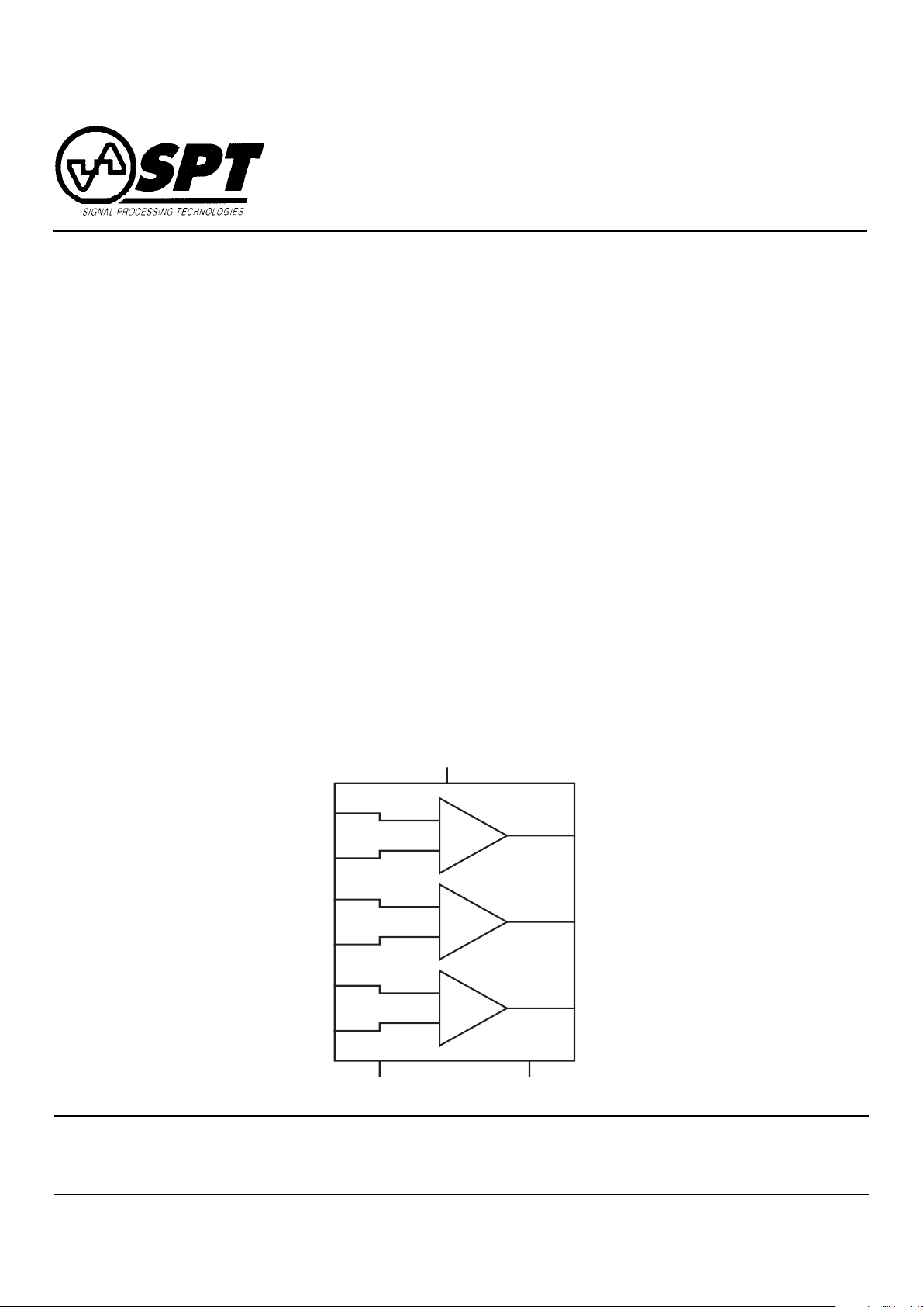
Driver
Driver
Driver
+ Input 1
- Input 1
+ Input 2
- Input 2
+ Input 3
- Input 3
Output 1
Output 2
Output 3
V
CC
Standby GND
BLOCK DIAGRAM
Page 2

SPT
2 8/24/98
SPT9402
ELECTRICAL SPECIFICATIONS
TA = +25 °C, V
CC
= +5.0 V, VIN = 1.0 V
P-P
video signal, voltage gain of +2, RL = 150 Ω, unless otherwise specified.
TEST TEST SPT9402
PARAMETERS CONDITIONS LEVEL MIN TYP MAX UNITS
Power Supply
Supply Current (ICC) No Input I 19 27 mA
V
CC
Voltage IV 4.5 5.0 5.5 V
Power Dissipation I 95 135 mW
Standby Current Pin 2 Grounded I 22.5 50 µA
Standby Power Dissipation Pin 2 Grounded I 113 250 µW
Digital Input
Digital Input (Low) Standby Pin 2 I 0.0 0.1 0.3 V
Digital Input (High) Standby Pin 2 I 1.8 2.0 V
CC
V
Dynamic Performance
Voltage Gain fIN = 1 MHz I 5.7 6.0 6.3 dB
Total Harmonic Distortion f
IN
= 1 kHz I 0.2 1.0 %
Open Loop Gain V 40 dB
Bandwidth V 20 MHz
Slew Rate V 70 V/µs
Frequency Response fIN = 1 to 5 MHz V -0.9 dB
Cross Talk f
IN
= 1 MHz V -40 dB
ABSOLUTE MAXIMUM RATINGS (Beyond which damage may occur)
(1)
25 °C
Supply Voltages
VCC.......................................................................+6.0 V
Maximum Power Dissipation
P
D
....................................................................................
350 mW
Thermal Impedance (TA=+25 °C and above)
Θ
CA
............................................................................
2.8 mW/°C
Temperature
Operating Temperature ................................. 0 to +70 °C
Storage Temperature................................-55 to +150 °C
Note: 1. Operation at any Absolute Maximum Rating is not implied. See Electrical Specifications for proper nominal
applied conditions in typical applications.
TEST PROCEDURE
100% production tested at the specified temperature.
100% production tested at TA = +25 °C, and sample tested
at the specified temperatures.
QA sample tested only at the specified temperatures.
Parameter is guaranteed (but not tested) by design and
characterization data.
Parameter is a typical value for information purposes only.
100% production tested at T
A
= +25 °C. Parameter is
guaranteed over specified temperature range.
TEST LEVEL
I
II
III
IV
V
VI
TEST LEVEL CODES
All electrical characteristics are subject to the following
conditions:
All parameters having min/max specifications are guaranteed. The Test Level column indicates the specific
device testing actually performed during production and
Quality Assurance inspection. Any blank section in the
data column indicates that the specification is not tested
at the specified condition.
Page 3

SPT
3 8/24/98
SPT9402
Figure 1 - Typical Interface Circuit (1 of 3 Drivers)
PACKAGE OUTLINE
12-Lead SSOP
INCHES MILLIMETERS
SYMBOL MIN MAX MIN MAX
A 0.165 0.181 4.2 4.6
B 0.189 0.205 4.8 5.2
C 0.012 typ 0.3 typ
D 0.031 typ 0.8 typ
E 0.000 0.008 0.0 0.2
F 0.047 0.063 1.2 1.6
G 0.067 max 1.7 max
H 0.264 0.248 6.7 6.3
I 0.004 0.010 0.10 0.25
J 0-10° 0-10°
K 0.012 0.028 0.3 0.7
L 0.047 typ 1.2 typ
M 0.016 typ 0.4 typ
N 0.031 typ 0.8 typ
O 0.213 typ 5.4 typ
A
B
C D
E
FG
H
I
J
K
Suggest ed P ad Layout
L
O
NM
Driver
V
CC
10 kΩ
+
10 kΩ
75 Ω
+
26
+
33 µF
VCC=5.0 V
GND
1
Input
5 kΩ5 kΩ
10 µF
Standby
4.7 µF
V
OUT
= 2.0 V
P-P
+
47 µF
Output
75 Ω
75 Ω Cable
+
-
0.01 µF
75 Ω
Page 4

SPT
4 8/24/98
SPT9402
PIN ASSIGNMENTS
PIN FUNCTIONS
Name Function
Input
1
Channel 1 Signal Input
(typically 1 V
P-P
, AC coupled)
Input
2
Channel 2 Signal Input
(typically 1 V
P-P
, AC coupled)
Input
3
Channel 3 Signal Input
(typically 1 V
P-P
, AC coupled)
Output
1
Channel 1 Output
(typically 2.0 V
P-P
, RL = 150 Ω, AC coupled)
Output
2
Channel 2 Output
(typically 2.0 V
P-P
, RL = 150 Ω, AC coupled)
Output
3
Channel 3 Output
(typically 2.0 V
P-P
, RL = 150 Ω, AC coupled)
Standby Power Down Standby Mode Select
(Low = Standby, Internal Pull-Up)
V
CC
+5.0 V Supply
GND Ground
ORDERING INFORMATION
PART NUMBER TEMPERATURE RANGE PACKAGE TYPE
SPT9402SCR 0 to +70 °C 12-Lead SSOP
Signal Processing Technologies, Inc. reserves the right to change products and specifications without notice. Permission is hereby expressly
granted to copy this literature for informational purposes only. Copying this material for any other use is strictly prohibited.
WARNING - LIFE SUPPORT APPLICATIONS POLICY - SPT products should not be used within Life Support Systems without the specific
written consent of SPT. A Life Support System is a product or system intended to support or sustain life which, if it fails, can be reasonably
expected to result in significant personal injury or death.
Signal Processing Technologies believes that ultrasonic cleaning of its products may damage the wire bonding, leading to device
failure. It is therefore not recommended, and exposure of a device to such a process will void the product warranty.
V
CC
Standby
+ Input 1
- Input 1
Output 1
GND
+ Input 3
- Input 3
Output 3
Output 2
- Input 2
+ Input 2
12
11
10
9
8
7
1
2
3
4
5
6
 Loading...