

Page 1
SPT9400
TRIPLE VIDEO DRIVER WITH Y/C & COMPOSITE OUTPUT
FEATURES
• Triple Video Line Driver Chip With Y/C Inputs
• Composite and Y/C Outputs
•RL = 150 Ω (75 Ω Back-Terminated Cable)
• Internal Clamping and Bias Circuitry
• Power-Down Standby Mode
• Very Small 5.0 x 4.4 mm Package
• Low Power Dissipation: 168 mW
•1 V
Input Range
P-P
• 6 dB Voltage Gain
• Flat Response fIN = 100 kHz to 10 MHz (typical)
• Crosstalk -40 dB (Typical)
• Single +5 Volt Power Supply
GENERAL DESCRIPTION
The SPT9400 is a triple video line driver chip that takes
standard Y/C analog inputs and provides simultaneous Y/C
and composite video analog outputs for driving 75 Ω lines.
Internal summing of the Y and C inputs is performed to
produce composite video output. It is possible to achieve
composite output on both the Y and CVBS outputs simultaneously by inputting a composite signal on the Y input. The
luminance input is clamped at 1.25 V and amplified 6 dB to
produce a 2 V
(typical) into a series 75 Ω resistor and 75 Ω
P-P
APPLICATIONS
• Video Editing Equipment
• Video Capture/Playback Cards
• Video Tape Recorders
• TV Monitor Sources
• Multimedia PCs
cable load. The internal 1.5 kΩ resistor provides gain compensation for low frequency signals. The chrominance input
is biased at 2.0 V and amplified 6 dB to produce a 1.2 V
(typical), into a series 75 Ω resistor and 75 Ω cable load.
The SPT9400 features a standby (active low) mode that
draws only 113 µW of power. Nominal power dissipation (no
input) is typically 168 mW. It requires a single +5 V supply,
operates over the commercial temperature range (0 to +70 °C)
and is available in a very small (5.0 x 4.4 mm) 12-lead Shrink
Small Outline Package (SSOP).
P-P
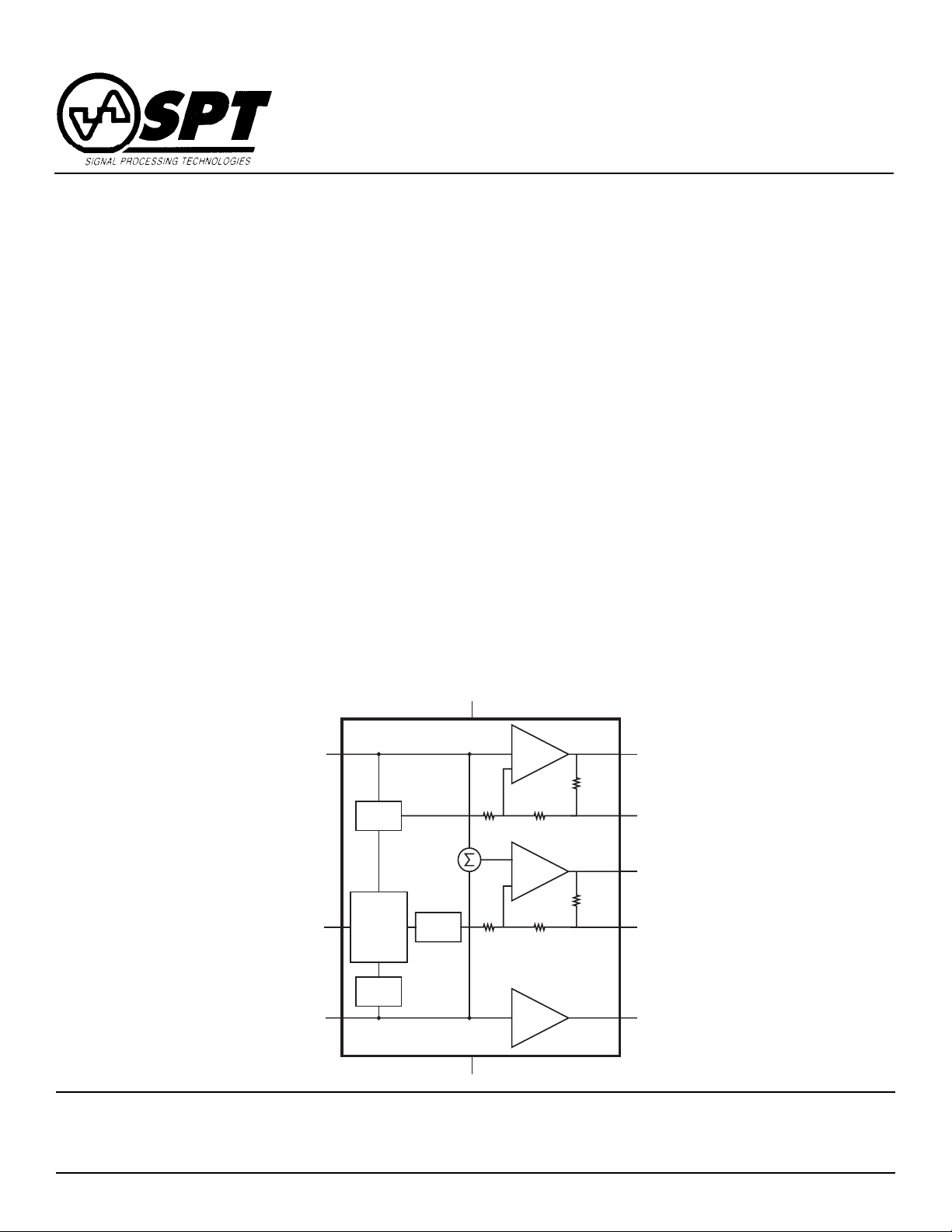
BLOCK DIAGRAM
Signal Processing Technologies, Inc.
+V
CC
Y Input Y Output
Clamp
1.25 V
Reference
Standby
C Input C Output
+
Standby
Logic
Bias
2.0 V
Clamp
1.25 V
GND
Driver
5 kΩ 5 kΩ
Driver
5 kΩ 5 kΩ
Driver
1.5 kΩ
Y Feedback
CVBS Output
1.5 kΩ
CVBS Feedback
4755 Forge Road, Colorado Springs, Colorado 80907, USA
Phone: (719) 528-2300 FAX: (719) 528-2370
Page 2

ABSOLUTE MAXIMUM RATINGS (Beyond which damage may occur)
(1)
25 °C
Supply Voltages
VCC.......................................................................+6.0 V
Maximum Power Dissipation
P
....................................................................................
D
350 mW
Temperature
Operating Temperature ................................. 0 to +70 °C
Storage Temperature................................-55 to +150 °C
Thermal Impedance (TA=+25 °C and above)
Θ
............................................................................
CA
2.8 mW/°C
Note: 1. Operation at any Absolute Maximum Rating is not implied. See Electrical Specifications for proper nominal
applied conditions in typical applications.
ELECTRICAL SPECIFICATIONS
TA = +25 °C, V
PARAMETERS CONDITIONS LEVEL MIN TYP MAX UNITS
Power Supply
Supply Current (ICC) No Input I 33.5 45 mA
V
Voltage IV 4.5 5.0 5.5 V
CC
Power Dissipation I 168 225 mW
Standby Current Pin 5 Grounded I 22.5 50 µA
Standby Power Dissipation Pin 5 Grounded I 113 µW
Digital Input
Digital Input (Low) Standby Pin 5 I 0.0 0.1 0.3 V
Digital Input (High) Standby Pin 5 I 1.8 2.0 V
Bias Voltages
Clamp Voltage Y Input Pin 2 I 1.05 1.25 1.45 V
Bias Voltage C Input Pin 6 I 1.7 2.0 2.3 V
Dynamic Performance
Voltage Gain I 5.5 6.0 6.5 dB
Differential Gain Ramp Input 3.58 MHz I -3.0 -1.5 +3.0 %
Differential Phase Ramp Input 3.58 MHz I -3.0 +0.2 +3.0 Degrees
Frequency Response f
Cross Talk Y
= +5.0 V, VIN = 1.0 V
CC
video signal, RL = 150 Ω, unless otherwise specified.
P-P
TEST TEST SPT9400
= 1 to 5 MHz V 0.0 dB
IN
to C
IN
CIN to Y
OUT
OUT
V -40 dB
V -40 dB
CC
V
TEST LEVEL CODES
All electrical characteristics are subject to the following
conditions:
All parameters having min/max specifications are guaranteed. The Test Level column indicates the specific
device testing actually performed during production and
Quality Assurance inspection. Any blank section in the
data column indicates that the specification is not tested
at the specified condition.
SPT
TEST LEVEL
I
II
III
IV
V
VI
2 8/24/98
TEST PROCEDURE
100% production tested at the specified temperature.
100% production tested at TA = +25 °C, and sample tested
at the specified temperatures.
QA sample tested only at the specified temperatures.
Parameter is guaranteed (but not tested) by design and
characterization data.
Parameter is a typical value for information purposes only.
100% production tested at T
guaranteed over specified temperature range.
= +25 °C. Parameter is
A
SPT9400
Page 3
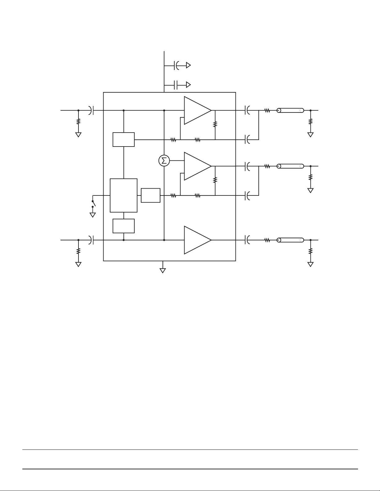
Figure 1 - Typical Interface Circuit
VCC = 5.0 V
33 µF
+
.01 µF
Y Input
1.0 V
C Input
0.6 V
P-P
P-P
75 Ω
Standby
75 Ω
4.7 µF
4.7 µF
+
+
2
Clamp
1.25 V
Reference
5
Standby
6
+
Logic
Bias
2.0 V
Clamp
1.25 V
1
5 kΩ 5 kΩ
5 kΩ 5 kΩ
3,4,7
6 dB
6 dB
6 dB
12
1.5 kΩ
11
10
1.5 kΩ
9
8
+
33 µF
+
33 µF
+
33 µF
+
33 µF
+
10 µF
75 Ω 75 Ω Cable
Y Output
75 Ω
75 Ω 75 Ω Cable
CVBS Output
75 Ω
75 Ω 75 Ω Cable
C Output
75 Ω
SPT
SPT9400
3 8/24/98
Page 4

Figure 2 - CVBS Output (Multiburst Test)
Figure 3 - CVBS Output (DP/DG)
SPT
SPT9400
4 8/24/98
Page 5

Figure 4 - CVBS Output (Vector Scope)
Figure 5 - CVBS Output (Bar and Line Time)
SPT
SPT9400
5 8/24/98
Page 6

PACKAGE OUTLINE
12-Lead SSOP
INCHES MILLIMETERS
SYMBOL MIN MAX MIN MAX
A 0.165 0.181 4.2 4.6
B 0.189 0.205 4.8 5.2
C 0.012 typ 0.3 typ
D 0.031 typ 0.8 typ
E 0.000 0.008 0.0 0.2
F 0.047 0.063 1.2 1.6
G 0.067 max 1.7 max
A
B
FG
J
K
NM
L
H 0.264 0.248 6.7 6.3
I 0.004 0.010 0.10 0.25
J 0-10° 0-10°
K 0.012 0.028 0.3 0.7
L 0.047 typ 1.2 typ
M 0.016 typ 0.4 typ
N 0.031 typ 0.8 typ
O 0.213 typ 5.4 typ
C D
H
E
I
Suggested Pad La you t
O
SPT
SPT9400
6 8/24/98
Page 7

PIN ASSIGNMENTS
V
1
CC
Y
2
IN
GND
GND
Standby
3
4
5
C
6
IN
12
11
10
9
8
7
Y
OUT
Y
FB
CVBS
CVBS
C
OUT
GND
OUT
FB
PIN FUNCTIONS
Name Function
Y
IN
C
IN
Standby Power Down Standby Mode Select (Low =
Y
OUT
Y
FB
CVBS
OUT
CVBS
FB
C
OUT
V
CC
GND Ground
Luminance (Y) Signal Input (typically
1 V
, AC coupled)
P-P
Chrominance (C) Signal Input (typically
0.62 V
, AC coupled)
P-P
Standby, Internal Pull-Up)
Luminance (Y) Output (typically 2.0 V
P-P
RL = 150 Ω, AC coupled)
Luminance Feedback Pin
Composite Video (CVBS) Output (typically
2.0 V
, RL = 150 Ω, AC coupled)
P-P
Composite Video Feedback Pin
Chrominance (C) Output (typically 1.3 V
P-P
RL = 150 Ω, AC coupled)
+5.0 V Supply
,
,
ORDERING INFORMATION
PART NUMBER TEMPERATURE RANGE PACKAGE TYPE
SPT9400SCR 0 to +70°C 12-Lead SSOP
Signal Processing Technologies, Inc. reserves the right to change products and specifications without notice. Permission is hereby expressly
granted to copy this literature for informational purposes only. Copying this material for any other use is strictly prohibited.
WARNING - LIFE SUPPORT APPLICATIONS POLICY - SPT products should not be used within Life Support Systems without the specific
written consent of SPT. A Life Support System is a product or system intended to support or sustain life which, if it fails, can be reasonably
expected to result in significant personal injury or death.
Signal Processing Technologies believes that ultrasonic cleaning of its products may damage the wire bonding, leading to device
failure. It is therefore not recommended, and exposure of a device to such a process will void the product warranty.
SPT9400
SPT
7 8/24/98
 Loading...