

Page 1

Signal Processing Technologies, Inc.
4755 Forge Road, Colorado Springs, Colorado 80907, USA
Phone: (719) 528-2300 FAX: (719) 528-2370
FEATURES
• NTSC/PAL Compatible
• Composite/S-Video Input Selection Mux
• Integrated Dual Analog Signal Path
• Adjustable Internal Anti-Alias Filters
• Internal Clamp Circuits
• Automatic Gain Control
• Integrated Reference Voltage Source for SPT7852
• Matched Voltage Output Range for Driving SPT7852
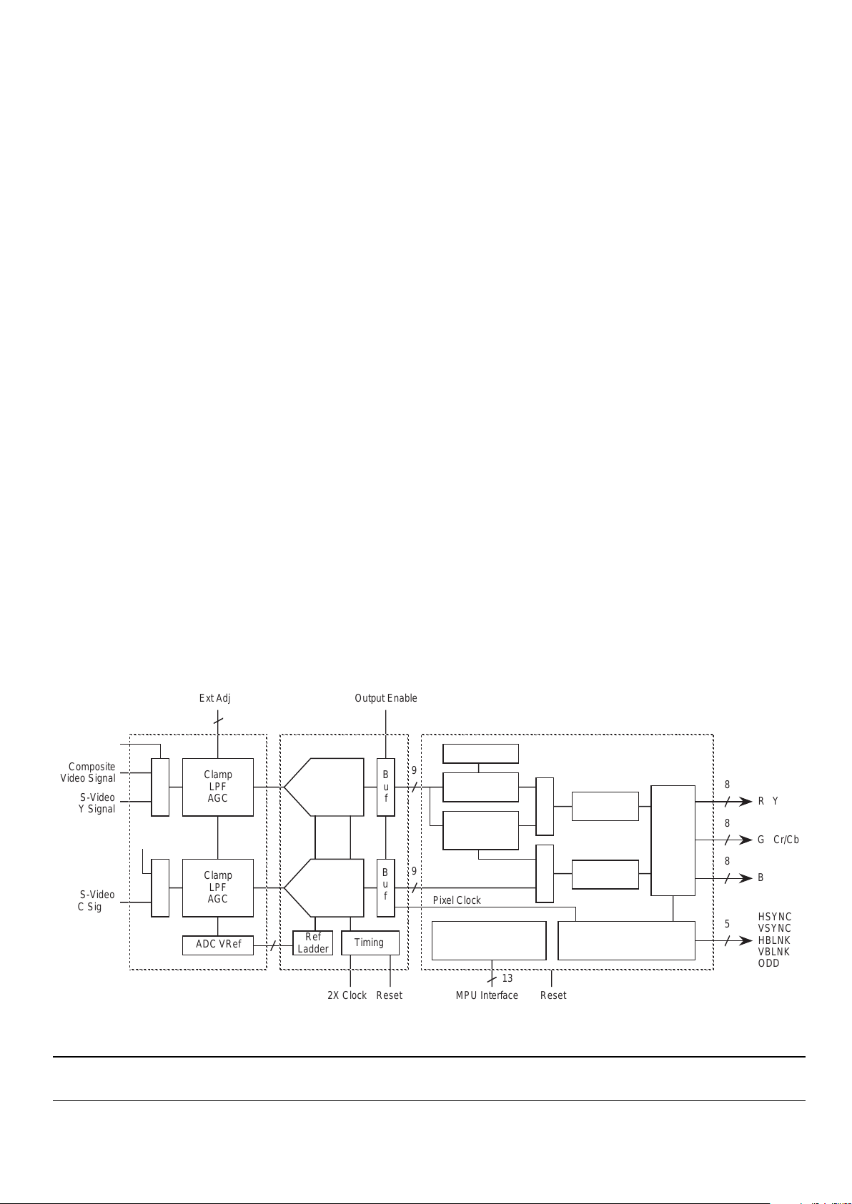
BLOCK DIAGRAM
APPLICATIONS
• High-End NTSC/PAL Video Decoding
• High Quality S-Video Decoding
• Video Frame Grabbing
• Professional Video
• VCR Signal Capture
• Security Cameras
GENERAL DESCRIPTION
The SPT9210 is the analog front-end processing chip for the
SPT video decoder chip set. The video decoder chip set is an
integrated three chip solution for high quality video signal
decoding of NTSC/PAL composite video and S-Video formats at 8.9 effective number of bits of dynamic performance.
The SPT9210 is a fully integrated analog video processor
chip capable of processing standard video signals in either a
single-channel composite video input mode or a dual-channel S-Video (component Y/C) input mode. As part of the chip
set, the SPT9210 is specially designed to easily interface to
the downstream SPT7852 dual 10-bit analog-to-digital converter (See figure 1.)
SPT9210
ANALOG VIDEO PROCESSOR
19
174 1810
2
3
20
9 7 8 12 13 11
Clamp
Clamp
Bias
Bias
SW
Low Pass
Filter
Low Pass
Filter
Sync
Separation
Automatic
Gain Control
Automatic
Gain Control
Gain Detect
Delay
Clamp
Clamp
3x
3x
Voltage Regulator
Frequency
Adjustment
Vref
1 16 15
14
6
5
Select SW
Input Y
Input C
Vcc
Input Y/C
GND Vref
Vref
Clamp
Filter Adj.
VRL
Adjust
VRL
Force
VRL
Sense
VRH
Sense
VRH
Force
VRH
Adjust
Output C
Output Y
C-Clamp C
C-AGC C-Clamp Y
The SPT9210 provides luminance and chrominance channel
DC restoration, anti-alias filtering, automatic gain control and
signal offset and gain to match the front-end requirements of
the SPT7852 dual 10-bit analog-to-digital converter.
In addition to performing the analog processing of the video
signal before data conversion, the SPT9210 also provides
the voltage reference sources for the SPT7852. The SPT9210
is available in a 20-lead SOIC package and operates over the
commercial temperature range. It requires a single +5 V
supply and dissipates 620 mW of power.
Page 2

SPT
2 11/7/97
SPT9210
ELECTRICAL SPECIFICATIONS
TA=+25 °C, VIN=1.0 V
P-P
, VCC=+5.0 V, unless otherwise specified.
TEST TEST
PARAMETERS CONDITIONS LEVEL MIN TYP MAX UNITS
Video Signal Output
Y/C Output Amplitude (pin 14) Composite/S-Video Mode 2.5 V
P-P
C Output Amplitude (pin 6) S-Video Mode 0.7 V
P-P
Differential Gain Composite/S-Video Mode 0.5 %
Differential Phase Composite/S-Video Mode 0.5 Degrees
Automatic Gain Control
Y/C Output Amplitude (pin 14) VIN=+3 dB 2.5 V
Composite/S-Video Mode
Y/C Output Amplitude (pin 14) V
IN
=-6 dB 2.5 V
Composite/S-Video Mode
C Output Amplitude (pin 6) VIN=+3 dB 0.7 V
S-Video Mode
C Output Amplitude (pin 6) VIN=-6 dB 0.7 V
S-Video Mode
Clamp Circuit
Sync Tip Offset Level Composite/S-Video Mode 1.0 V
C Output Bias Voltage S-Video Mode 2.5 V
Anti-Alias Filter Chrominance Signal Side
Frequency Response f
IN
=3 MHz, VIN=0 dB 7.96 dB
Frequency Response fIN=5 MHz, VIN=0 dB 4.96 dB
Voltage Reference
V
RH
(Top of Ladder) I
OUT
=+5 mA 3.6 V
VRL(Bottom of Ladder) I
OUT
=+5 mA 1.0 V
Digital Input (Select SW pin 1)
Logic 1 Voltage 2.0 V
Logic 0 Voltage 0.8 V
Power Supply
Supply Current I
CC
No Signal 70 mA
Supply Voltage V
CC
4.75 5.75 V
ABSOLUTE MAXIMUM RATINGS (Beyond which damage may occur)
1
Supply Voltage
VCC...........................................................................+6 V
Temperature
Operating Temperature ................................. 0 to +70 °C
Junction Temperature ......................................... +175 °C
Lead Temperature, (soldering 3 seconds).......... +320 °C
Storage Temperature................................ -55 to +150 °C
Note: 1. Operation at any Absolute Maximum Rating is not implied. See Electrical Specifications for proper nominal
applied conditions in typical applications.
TEST LEVEL CODES
All electrical characteristics are subject to the following conditions: All parameters having min/max specifications are guaranteed. The Test Level column
indicates the specific device testing actually performed during production and Quality Assurance inspection. Any blank section in the data column indicates that the specification is not tested at the specified condition.
TEST PROCEDURE
100% production tested at the specified temperature.
100% production tested at TA = +25 °C, and sample tested
at the specified temperatures.
QA sample tested only at the specified temperatures.
Parameter is guaranteed (but not tested) by design and
characterization data.
Parameter is a typical value for information purposes only.
100% production tested at TA = +25 °C. Parameter is
guaranteed over specified temperature range.
TEST LEVEL
I
II
III
IV
V
VI
Page 3
SPT
3 11/7/97
SPT9210
Figure 1 - SPT Video Decoder Chip Set
SPT VIDEO CHIP SET APPLICATION
The SPT9210 is the front-end analog video processor for the
SPT NTSC/PAL video decoder chip set. This chip set, as
shown in figure 1, is comprised of three monolithic chips, which
together provide an overall integrated video decoding functionality at 8.9 effective number of bits of dynamic performance.
The full set includes the SPT9210 analog video processor,
the SPT7852 dual 10-bit analog-to-digital converter and the
SPT2110 NTSC/PAL video decoder. The SPT9210 is specifically designed to process video input signals so as to attain
optimal data conversion by the SPT7852 analog-to-digital
converter. Data sheets describing the overall chip set and the
other components are available by contacting the factory.
SPT9210 GENERAL DESCRIPTION
The SPT9210 is a fully integrated analog video processor
chip capable of processing standard video signals in either a
single-channel composite video input mode or a dual-channel S-Video input mode. Standard 1 V
P-P
video signals are
amplified to match the optimal drive requirements of the
SPT7852 dual 10-bit analog-to-digital converter.
INPUT SELECTION
As the typical interface circuit shows in figure 3, the mux
selector pin (pin 1) controls selection between composite and
S-Video (component Y/C). This is a TTL-level input. When
composite video is selected (pin 1 high), the composite signal
(pin 19) is fed into the luminance channel, and the chrominance channel is internally biased (i.e., no input is sourced).
When S-Video is selected (pin 1 low), the S-Video luminance
signal (pin 2) is fed into the luminance channel, and the SVideo chrominance signal (pin 3) is fed into the chrominance
channel.
In addition to pin 19, another composite video signal can be
applied to input pin 2. Pin 1 selects which video signal is to be
processed. (Pin 1 high selects input from pin 19.) When
operating with composite video on pin 2, decouple pin 3 to
ground with a 0.1 µF capacitor (the chrominance input for Svideo). This will reduce the noise produced on this input.
A register or TTL buffer can drive pin 1 (video select switch).
An optional transistor circuit is shown in figure 3. It is driven
by the pin 1 signal with the collector tied to pin 3. It is used to
reduce crosstalk that may occur when both composite and SVideo signals are operating simultaneously. The transistor
circuit is only necessary if both signals are present.
All input video signals should be terminated with 75 Ω
resistors and AC coupled to the SPT9210 with a 0.47 µF
capacitor.
INTERNAL CLAMP, BIAS AND SYNC DETECTION
The signals fed into the luminance channel (pins 2 and 19),
which are either a composite signal or a luminance (Y) signal,
are internally DC restored to 2.0 V by an internal clamp circuit.
Note that this is not the final output clamp voltage as discussed in the Final DC Clamp and Gain Stages section. The
chrominance signal (pin 3) is biased to 2.5 V by an internal
bias circuit.
The luminance signal path has a sync separation circuit that
compares the sync signal to a detection threshold and
generates internal gain control and output clamping control
signals. These timing signals are used to control internal
sampling of the sync tip amplitude by the automatic gain
control circuit. (See the Automatic Gain Control discussion.)
Trap Filter
Y/C Separator
(Comb)
Luma
Processing
Chroma
Processing
Timing Generation
Control Parameter
Registers
Color Space
Conversion
10-Bit ADC
10-Bit ADC
2X Clock MPU Interface
HSYNC
VSYNC
HBLNK
VBLNK
ODD
9
9
B
u
f
B
u
f
Output Enable
Reset
Ref
Ladder
Timing
Pixel Clock
Reset
13
R Y
G Cr/Cb
B
5
8
8
8
Ext Adj
Clamp
LPF
AGC
Clamp
LPF
AGC
ADC VRef
Composite
Video Signal
S-Video
Y Signal
S-Video
C Signal
Select
2
5
Bias
Sync Det
SPT2110SPT7852SPT9210
M
u
x
M
u
x
M
u
x
M
u
x
Page 4
SPT
4 11/7/97
SPT9210
ANTI-ALIAS FILTERS
Both luminance and chrominance video signal paths have an
anti-alias filter with a cut-off frequency of approximately
4.8 MHz. The cut-off frequency can be changed by an
external resistor value. The relationship between the external
resistance value and the cut-off frequency is shown in the
Typical Performance Curves section.
AUTOMATIC GAIN CONTROL
The SPT9210 performs automatic gain control (AGC) of the
composite/luminance and chrominance signals. The horizontal sync signal level is used as a reference for control of
the signal gain. The chrominance signal gain is slaved to the
luminance gain value.
The gain circuitry can operate over an input voltage range of
VIN = -6 dB to +3 dB (where 1 V
P-P
= 0 dB). The AGC will
maintain a 2.5 V
P-P
amplitude on the composite/luminance
signal output and 0.7 V
P-P
amplitude on the chrominance
signal output. The AGC settling time can be adjusted via an
external capacitor. SPT recommends using a 0.47 µF capacitor for most conditions. In cases where extreme fluctuation is
possible, a diode inserted between pins 7 and 16 will restrict
the maximum control voltage. This will serve to reduce
recovery time.
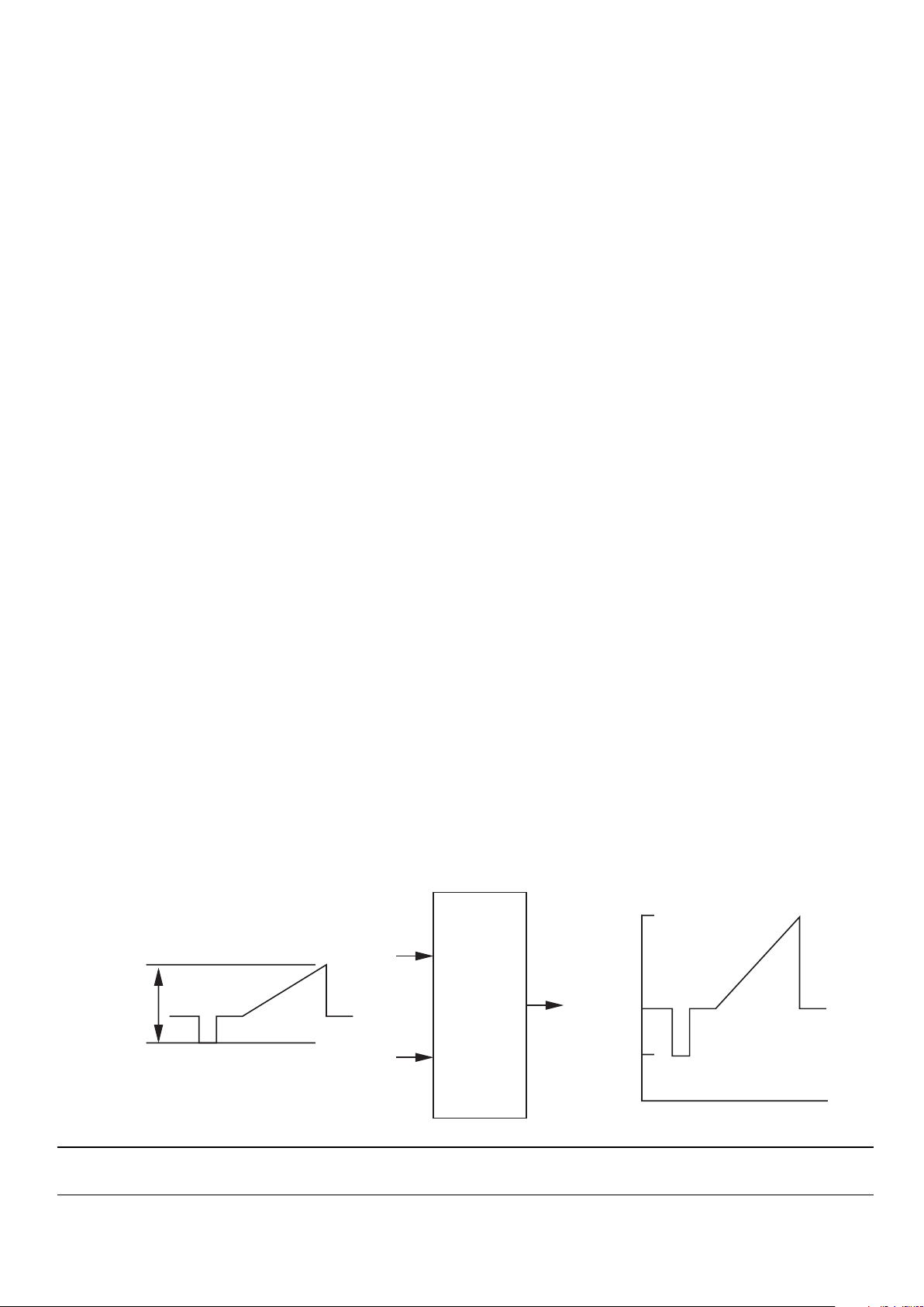
FINAL DC CLAMP AND GAIN STAGES
After the clamp, low pass filtering and automatic gain control
functions are performed. Each signal path is clamped to a fixed
DC value and amplified to the proper voltage range for input
into the SPT7852 analog-to-digital converter. The analog sync
signal is retained in the output of the SPT9210 and passed on
to the SPT7852 and SPT2110 NTSC/PAL video decoder.
For the composite/luminance output, the horizontal sync
level is clamped to +1 V, and the full-scale amplitude of the
composite luminance signal (including sync tip) is set to
2.5 V
P-P
amplitude by the AGC. (See figure 2.) The generated
signal is optimized for SPT7852 performance (+1.0 to +3.5 V
input range). The chrominance output signal is biased to
+2.5 V and a 0.7 V
P-P
full-scale amplitude is maintained by
the AGC.
The output drive circuit is optimized for interface to the
SPT7852. When driving loads other than the SPT7852 (which
have a capacitance >TBD µF), it may be necessary to insert
a series resister between the output and the load so as to
avoid oscillation.
ON-CHIP VOLTAGE REFERENCES
In addition to performing the analog processing of the video
signal before data conversion, the SPT9210 also provides
the voltage reference sources (force and sense for the top
and bottom of the reference ladder) required by the SPT7852.
This eliminates the need for external reference sources. A
source of +3.5 V is provided to the top of the reference ladder
and +1.0 V is provided to the bottom.
Pin 7 is the VL reference force pin and is tied to pin 4 of the
SPT7852. Pin 13 is the VH reference force pin and is tied to
pin 1 of the SPT7852. A 240 Ω resistor should be tied between
pin 7 and pin 13 on the SPT9210. Pin 8 is the VL reference
sense pin and is tied to pin 3 of the SPT7852. Pin 8 is the V
H
reference sense pin and is tied to pin 2 of the SPT7852.
The values of VL and VH can be adjusted by changing the
external resistor values at pins 9 and 11, respectively. The
curves in the Typical Performance Curve section show the
voltage reference output values versus the external resistance values. The typical values for nominal +1.0 V and
+3.5 V operation on VL and VH are approximately 10 kΩ and
25 kΩ, respectively.
The V
Ref
clamp pins need decoupling capacitors as shown in
figure 3. Each pin should have a 0.1 µF and 10 µF capacitor
connected in parallel for proper decoupling.
OTHER INFORMATION
The SPT9210 is available in a 20-lead SOIC package and
operates over the commercial temperature range. It requires
a single +5 V supply and dissipates 620 mW of power.
Figure 2 - Composite/Luminance Signal I/O Relationship
1.0 Vpp
SPT9210
3.5 V
1.0 V
0.0 V
Pin 2
Pin 19
Pin 14
Input Signal Output Signal
Composite
Signal
Y Signal
Composite/Y
Output
Page 5

SPT
5 11/7/97
SPT9210
Figure 3 - Typical Interface Circuit
1
9
+A
5
10
µF
1
7
4
1
8
1
0
2
3
2
0
75
Ω
0.47
µF
75
Ω
0.47
µF
75
Ω
0.47
µF
9
8
1
3
1
1
5
kΩ
10 kΩ
Clam
p
Clam
p
Bia
s
Bia
s
SW
Low Pass
Filter
Low Pass
Filter
Sync
Separation
Automatic
Gain Control
Automatic
Gain Control
Gain
Detect
Dela
y
Clam
p
Clam
p
3
x
3
x
Voltage
Regulator
Frequency
Adjustment
V
Re
f
1
1
6
1
5
1
4
6
5
25
kΩ
C-Clamp-Y
0.68 µF
500
kΩ
to V
RL
Pin 7
(SPT9210)
0.47 µF
High: Composite
Low: S-Video
V
IN
= 1.0 V
P-
P
Composite
Signal Input
S-Video
Y-Signal Input
S-Video
C-Signal Input
V
Re
f
V
Ref
Clamp
Filter-
Adj
V
RL
Adj
V
RL
Sense
to
SPT7852
Pin 3
V
RL
Force
to
SPT7852
Pin 1
240
Ω
C-Clamp-C
0.68 µF
500
kΩ
C-Signal Output
To SPT7852
Pin 8
Y/C-Signal Output
To SPT7852
Pin 6
Vcc
100
Ω
4.7
kΩ
Buffe
r
C-AGC
1N91
4
1
2
V
RL
Sense
to SPT7852
Pin 2
7
V
RL
Force
to
SPT7852
Pin 4
V
RH
Adj
GN
D
*
*
* 0.1 µF and 10 µF in parallel
‡ Optional ciruit (see text)
*
*
‡
Page 6

SPT
6 11/7/97
SPT9210
TERMINAL EXPLANATIONS
Pin Name Voltage
1 Select SW 1.4 V
When this terminal is open or
high, it is in the composite
mode. When this terminal is
low, it is in the S-Video mode.
Pin Name Voltage
2 Input Y 2.0 V
This terminal is the luminance
signal input of the S-Video
mode. The clamp circuit fixes
the sync/bottom voltage to
2.0 V.
Pin Name Voltage
3 Input C 2.5 V
This terminal is the
chrominance signal input for
S-Video mode. The bias circuit
fixes the center voltage to
2.5 V.
Pin Name Voltage
4V
Ref
2.5 V
This terminal is the bypass
capacitor connection for the
internal reference voltage
circuit.
5 kΩ 2 kΩ
V
CC
50 µA
1
2
VCCVCCVCCVCCV
CC
V_Clamp =
2.0 V
+
-
VCCVCCV
CC
3
V
REF
=
2.5 V
1 kΩ
+
-
4
VCCVCCV
CC
10 kΩ
40 kΩ
V_BG =
1.2 V
Pin Name Voltage
5 C-Clamp C 1.5 V
This terminal connects the
capacitor that determines the
time constant of the
chrominance clamp circuit.
Pin Name Voltage
6 Output C 2.5 V
This terminal is the
chrominance signal output.
Pin Name Voltage
7 VRL Force 1.0 V
8 VRL Sense 1.0 V
9 VRL Adjust 0.6 V
These terminals are the
reference voltage sources for
the ADC on the low side.
They are the output, sense
and adjustment terminals.
V
CC
5
+
-
+
-
CLK Signal
Clamp
Voltage
From
AGC
10 kΩ
2 kΩ
2 kΩ
To Final
Amp
V
CC
+
-
6
+
-
V
CC
AGC
Clamp
6 kΩ
3 kΩ
4.8 mA
V
CC
V
CC
7
7.5 kΩ
15 kΩ
V
CC
V_BG =
1.2 V
V
CC
89
Buffer
Amp
+
-
Page 7

SPT
7 11/7/97
SPT9210
TERMINAL EXPLANATIONS - CONTINUED
Pin Name Voltage
10 Ground 0.0 V
Pin Name Voltage
11 V
RH
Adjust 3.6 V
12 VRL Sense 3.6 V
13 VRL Force 3.6 V
These terminals are the
reference voltage sources for
the ADC on the high side.
They are the output, sense
and adjustment terminals.
Pin Name Voltage
14 Output Y 2.5 V
This terminal is the luminance
signal output.
Pin Name Voltage
15 C-Clamp Y 0.6 V
This terminal connects the
capacitor that determines the
time constant of the luminance
clamp circuit.
Pin Name Voltage
16 C-AGC 0.6 V
This terminal connects the
capacitor that determines the
time constant of the AGC
circuit.
Pin Name Voltage
17 Filter Adjust 0.7 V
This terminal is the fc
adjustment of the internal
low pass filter.
Pin Name Voltage
18 V
Ref
Clamp 2.0 V
This terminal is the bypass
capacitor connection for the
internal reference voltage
circuit.
Pin Name Voltage
19 Input Y/C 2.0 V
This terminal is the input of
the composite signal. The
clamp circuit fixes the sync/
bottom voltage to 2.0 V.
Pin Name Voltage
20 V
CC
5.0 V
This terminal is the power
supply.
Inner
Voltage
Reference
(2.0 V)
V
CC
25.5 kΩ
30 kΩ
V
CCVCC
11 1312
Buffer
Amp
+
-
V
CC
1.7 kΩ20 kΩ
14
+
-
V
CC
AGC
Clamp
6 kΩ
3 kΩ
4.8 mA
V
CC
V
CC
15
+
-
+
-
CLK Signal
Clamp
Voltage
From
AGC
10 kΩ
2 kΩ
2 kΩ
To Final
Amp
V
CC
+
-
V
CC
16
+
-
+
-
DLY Signal
AGC
Voltage
10 kΩ
3.6 kΩ
+
-
VCCV
CC
Clamp
To Final
Amp
To AGC
V
CC
7 kΩ
V
CC
V_BG =
1.2 V
V
CC
17
V
CC
To Filter
Control
V
CC
V
CC
Inner Voltage
Reference
(2.0 V)
V
CC
18
19
VCCVCCVCCVCCV
CC
V_Clamp =
2.0 V
+
-
Page 8

SPT
8 11/7/97
SPT9210
S-Video VIN vs Sync, Bar
0
20
60
80
100
120
-6 -4 -2 0 +2
Sync, Bar (IRE)
VIN (dB)
40
Bar
Sync
Composite VIN vs Sync, Bar
0
20
60
80
100
120
-6 -4 -2 0 +2
Sync, Bar (IRE)
VIN (dB)
40
Bar
Sync
TYPICAL PERFORMANCE CURVES
Radj vs VRH (Pin 12)
3.2
3.3
3.4
3.5
3.6
3.7
0 20406080100
V
RH
(V)
Radj (kΩ)
Radj vs VRL (Pin 8)
0.8
0.9
1.0
1.1
1.2
1.3
0 20406080100
V
RL
(V)
Radj (kΩ)
Reference Voltage Characteristics
Video Signal Characteristics
Page 9

SPT
9 11/7/97
SPT9210
fIN vs Delay, Gain
-150
-50
+50
+150
+250
0.1 1 10 100
Delay (nsec)
fIN (MHz)
Gain
Delay
-70
-50
-30
-10
+10
Gain (dB)
TYPICAL PERFORMANCE CURVES
VIN vs Differential Phase
-2.0
-1.0
0
+1.0
+2.0
-6 -4 -2 0 +2
DP (Degrees)
VIN (dB)
S-Video
Composite
fIN vs V
OUT
-30
-20
-10
0
+10
0.1 1 10 100
V
OUT
(dB)
fIN (MHz)
0k
5k
10k
20k
30k
VIN vs Differential Gain
-20
-15
-10
-5
0
5
-6 -4 -2 0 +2
DG (%)
VIN (dB)
S-Video
Composite
Low-Pass Filter Characteristics
Page 10

SPT
10 11/7/97
SPT9210
1
20
C
G
A B
DE
F
H
I
PACKAGE OUTLINE
20-LEAD SOIC
INCHES MILLIMETERS
SYMBOL MIN MAX MIN MAX
A 0.165 0.181 4.2 4.6
B 0.224 0.248 5.7 6.3
C 0.394 0.409 10.0 10.4
D 0.039 typ 1.0 typ
E 0.010 0.018 0.25 0.45
F 0.000 0.008 0.0 0.2
G 0.047 0.071 1.2 1.8
H 0.002 0.010 0.05 0.25
I 0.012 0.028 0.3 0.7
Page 11

SPT
11 11/7/97
SPT9210
Signal Processing Technologies, Inc. reserves the right to change products and specifications without notice. Permission is hereby expressly
granted to copy this literature for informational purposes only. Copying this material for any other use is strictly prohibited.
WARNING - LIFE SUPPORT APPLICATIONS POLICY - SPT products should not be used within Life Support Systems without the specific
written consent of SPT. A Life Support System is a product or system intended to support or sustain life which, if it fails, can be reasonably
expected to result in significant personal injury or death.
Signal Processing Technologies believes that ultrasonic cleaning of its products may damage the wire bonding, leading to device
failure. It is therefore not recommended, and exposure of a device to such a process will void the product warranty.
NAME I/O FUNCTION
Select I Selects Video Input Source (High =
Composite Video or Low = S-Video)
Input Y I Luminance Signal Input
Input C I Chrominance Signal Input
V
Ref
- Internal Reference By-Pass
C-Clamp C I Chrominance Clamp Time
Constant Capacitor
Output C O Chrominance Signal Output
VRL Force O Voltage Reference Low Output
(Force)
VRL Sense O Voltage Reference Low Output
(Sense)
VRL Adjust I Voltage Reference Low Adjustment
GND I Ground
VRH Force O Voltage Reference High Output
(Force)
VRH Sense O Voltage Reference High Output
(Sense)
VRH Adjust I Voltage Reference High Adjust-
ment
Output Y O Luminance Signal Output
C-Clamp Y I Luminance Clamp Time Constant
Capacitor
C-AGC I Automatic Gain Control Time
Constant Capacitor
Filter Adj. I Adjustment For Fc of Low Pass
Filter
V
Ref
Clamp - Internal Reference Bypass
Input Y/C I Composite Signal Input
V
CC
I +5 V Power Supply
PIN FUNCTIONS
VRH Force
Output Y
1
2
3
16
15
14
4
5
6
7
8
9
10
11
12
13
17
18
19
20
V
Ref
Clamp
Filter Adjust
C-Clamp Y
C-AGC
VRH Adjust
VRH Sense
V
CC
Input Y/C
Input C
V
Ref
Output C
VRL Force
VRL Sense
C-Clamp C
GND
VRL Adjust
Select
Input Y
PIN ASSIGNMENTS
20L SOIC
ORDERING INFORMATION
PART NUMBER DESCRIPTION TEMPERATURE RANGE PACKAGE TYPE
SPT9210SCS Analog Video Processor 0 to +70 °C 20L SOIC
 Loading...