

Page 1
SPT9110
100 MSPS SINGLE-TO-DIFFERENTIAL TRACK-AND-HOLD
FEATURES
• 400 MHz Sampling Bandwidth
• 100 MHz Sampling Rate
• Excellent Hold Mode Distortion
-66 dB @ 50 MSPS (fIN = 25 MHz)
-58 dB @ 100 MSPS (fIN = 50 MHz)
• Track Mode Slew Rate: 700 V/µs
• Low Power: 120 mW Differential Mode
75 mW Single-Ended Mode
• Single +5 V Supply
• Internal +2.5 V Reference
GENERAL DESCRIPTION
The SPT9110 is a single-to-differential track-and-hold amplifier. It can be operated as a single-end THA only or, in full
configuration, as a single-to-differential THA. An internal
reference provides the common-mode voltage for the singleto-differential output stage. The THA, inverter and reference
have separate power supply pins so each can be optionally
powered up and used.
APPLICATIONS
• THA for Differential ADCs
• RF Demodulation Systems
• Test Instrumentation
• Digital Sampling Oscilloscopes
This device provides an analog designer with a low cost
single-to-differential THA amplifier for interfacing differential
and single-ended ADCs.
The SPT9110 is offered in a 28-lead SOIC package in the
industrial temperature range.
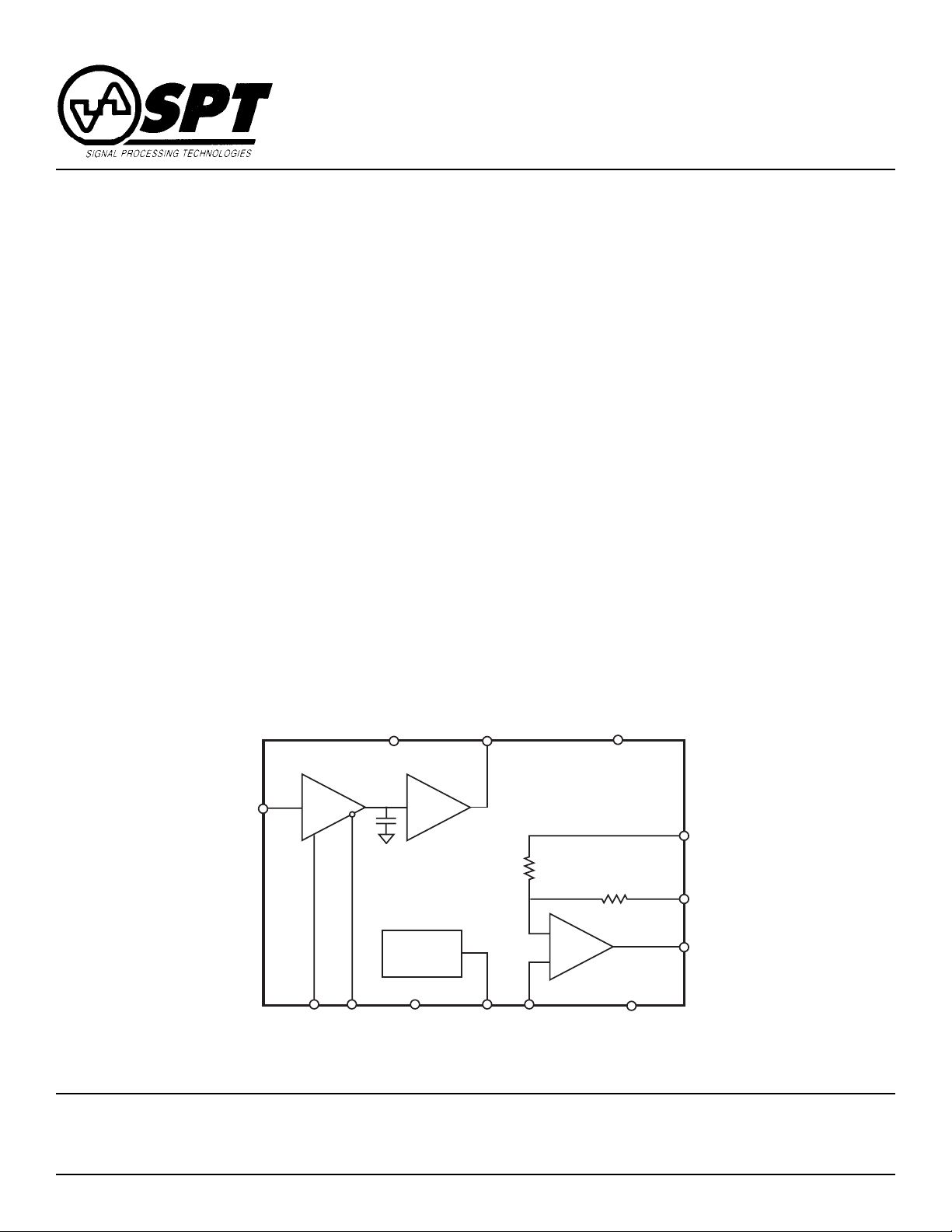
BLOCK DIAGRAM
Analog In
(VIN)
Signal Processing Technologies, Inc.
AV
CC
(THA)
1X 1X
C
OLD
H
Out+
1 kΩ
R1
AV
(INV)
CC
1 kΩ
R2
+2.5 V
-
CLK NCLK
Reference
AV
CC
(Ref)
Ref
Out
Ref
In
+
AGND
4755 Forge Road, Colorado Springs, Colorado 80907, USA
Phone: (719) 528-2300 FAX: (719) 528-2370
Invert In
Invert In
Out-
A
B
Page 2

ABSOLUTE MAXIMUM RATING (Beyond which damage may occur)
Supply Voltages
AVCC Supplies ............................................. -0.5 to +6 V
Output Currents
Continuous Output Current .................................±15 mA
2
1
Input Voltages
Analog Input Voltage .................................... -0.5 to +6 V
CLK, NCLK Input .......................................... -0.5 to +6 V
Ref In ............................................................ -0.5 to +6 V
Temperature
Operating Temperature ..............................-40 to +85 °C
Junction Temperature ......................................... +150 °C
Lead, Soldering (10 seconds)............................. +220 °C
Storage .....................................................-65 to +150 °C
Note 1: Operation at any Absolute Maximum Ratings is not implied. See Electrical Specifications for proper nominal
applied conditions in typical application.
Note 2: Outputs are short circuit protected.
ELECTRICAL SPECIFICATIONS
AVCC = +5.0 V, AGND = 0.0 V, Output Load = 1 kΩ and 10 pF, VIN = 2.0 Vp-p,Internal Reference, unless otherwise specified.
TEST TEST SPT9110
PARAMETERS CONDITIONS LEVEL MIN TYP MAX UNITS
DC Performance
Gain ∆V
Single Ended Out +25 °C I 0.95 0.97 0.99 V/V
Differential Out +25 °C I 1.80 1.93 2.00 V/V
Offset V
Out+ +25 °C I -100 ±50 +100 mV
Differential
Output Drive Capacity
Output Load at 10 pF Full Temperature V 1 kΩ
= 2.0 Vp-p
IN
= +2.5 V
IN
1
Full Temperature V 0.96 V/V
Full Temperature V 1.92 V/V
Full Temperature V 55 mV
+25 °C, Ref In=Out+ CM I -15 ±5 ±15 mV
Full Temperature V 10 mV
2
Full Temperature IV ±1 ±10 mA
Analog Input/Output
Output Voltage Range Full Temperature VI 1.5 3.5 V
Input Capacitance +25 °CV 5pF
Input Resistance +25 °C I 100 140 kΩ
Reference Voltage Output I 2.35 2.45 2.55 V
Reference Output Current
Reference Voltage Tempco Full Temperature V 75 ppm/°C
Clock Inputs
Input Type/Logic Family V Differential PECL
Input Bias Current +25 °CI 210µA
Input Low Voltage (Differential) +25 °C I 3.3 3.5 V
Input High Voltage (differential) +25 °C I 3.9 4.1 V
1
Differential offset is specified with Ref In equal to the common mode output voltage of OUT+ and so includes the offset error of the
inverter only.
2
This part is intended to drive a high impedance load. AC performance is degraded at ±10 mA. See the Typical Performance Graphs.
3
Ref Out has a typical output impedance of 1 kΩ and should be buffered for driving loads other than Ref In.
3
+25 °CV±100 µA
SPT
SPT9110
2 11/12/98
Page 3
ELECTRICAL SPECIFICATIONS
AVCC = +5.0 V, AGND = 0.0 V, Output Load = 1 kΩ and 10 pF, VIN = 2.0 Vp-p,Internal Reference, unless otherwise specified.
TEST TEST SPT9110
PARAMETERS CONDITIONS LEVEL MIN TYP MAX UNITS
Track Mode Dynamics
Bandwidth (-3 dB) +25 °C
Single Ended Out V 220 MHz
Differential Out V 140 MHz
Slew Rate 2.0 Vp-p Output Step +25 °C
Single Ended Out 20 pF Load IV 580 V/µs
Differential Out
Input RMS Spectral Noise Single Ended V 3.5
Track-to-Hold Switching
Aperture Delay +25 °C V 250 ps
Aperture Jitter +25 °C V <1 ps rms
Pedestal Offset +25 °CIV±12 mV
Hold Mode Dynamics
Worst Harmonic
5 MHz, 50 MSPS, Single-Ended TA = +25 °C IV -64 -68 dB
Worst Harmonic
5 MHz, 50 MSPS, Differential TA = +25 °C IV -61 -65 dB
Worst Harmonic
25 MHz, 50 MSPS, Single-Ended TA = +25 °C V -66 dB
Worst Harmonic
25 MHz, 50 MSPS, Differential TA = +25 °C V -64 dB
Worst Harmonic
50 MHz, 100 MSPS, Single-Ended TA = +25 °C IV -54 -58 dB
Worst Harmonic
50 MHz, 100 MSPS, Differential TA = +25 °C IV -50 -54 dB
Sampling Bandwidth5 (-3 dB) +25 °C V 400 MHz
VIN = 2.0 Vp-p
Hold Noise6 (RMS) +25 °C V 300 x t
Droop Rate, V
Feedthrough Rejection (50 MHz) Full Temperature V -65 dB
VIN= 2 Vp-p
7
4
(VIN = 1 Vp-p)
= +2.5 V +25 °CIV±40 mV/µs
IN
20 pF Load IV 800 V/µs
Differential V 13.0
Full Temperature V ±12 mV
TA = -40 °C to +85 °C V -64 dB
TA = -40 °C to +85 °C V -63 dB
TA = -40 °C to +85 °C V -63 dB
TA = -40 °C to +85 °C V -60 dB
TA = -40 °C to +85 °C V -54 dB
TA = -40 °C to +85 °C V -50 dB
H
Full Temperature IV ±80 mV/µs
nV/ Hz
nV/ Hz
mV/s
4. For hold times longer than 50 ns, the input common mode voltage may affect the hold mode distortion. (This is due to nonlinear
droop that varies with VCM.) For optimal performance, SPT recommends that the held output signal be used within 50 ns of the
application of the hold signal.
5. Sampling bandwidth is defined as the -3 dB frequency response of the input sampler to the hold capacitor when operating in the
sampling mode. It is greater than tracking bandwidth because it does not include the bandwidth of the output amplifier.
6. Hold mode noise is proportional to the length of time a signal is held. This value must be combined with the track mode noise to
obtain total noise.
7. Optimized for hold mode performance and low power.
SPT9110
SPT
3 11/12/98
Page 4

ELECTRICAL SPECIFICATIONS
AVCC = +5.0 V, AGND = 0.0 V, R
PARAMETERS CONDITIONS LEVEL MIN TYP MAX UNITS
Hold-to-Track Switching
Acquisition Time to 0.1% +25 °C V 3.5 ns
1 V Output Step
Acquisition Time to 0.025% +25 °C V 4.0 ns
1 V Output Step
Power Supplies
Supply Voltage IV 4.75 5 5.25 V
Supply Current
Single Ended Output Mode
Differential Output Mode I 24 30 mA
Power Dissipation
Single Ended Output Mode
Differential Output Mode I 120 150 mW
Power Supply Rejection Ratio +25 °C V 44 dB
Single-Ended Output ∆VCC = 0.5 V
8. Measured at the hold capacitor.
9. Inverter powered down.
8
TEST LEVEL CODES
All electrical characteristics are subject to the
following conditions: All parameters having min/
max specifications are guaranteed. The Test
Level column indicates the specific device testing actually performed during production and
Quality Assurance inspection. Any blank section in the data column indicates that the specification is not tested at the specified condition.
= 1 kΩ and 10 pF, VIN = 2.0 Vp-p, Internal Reference, unless otherwise specified.
Load
TEST TEST SPT9110
9I
9I
P-P
TEST LEVEL
I
II
TEST PROCEDURE
100% production tested at the specified temperature.
100% production tested at TA = +25 °C, and sample
15 20 mA
75 100 mW
tested at the specified temperatures.
III
IV
QA sample tested only at the specified temperatures.
Parameter is guaranteed (but not tested) by design
and characterization data.
V
Parameter is a typical value for information purposes
only.
VI
100% production tested at TA = +25 °C. Parameter is
guaranteed over specified temperature range.
SPT
SPT9110
4 11/12/98
Page 5

TIMING SPECIFICATION DEFINITIONS
TRACK-TO-HOLD SETTLING TIME
ACQUISITION TIME
This is the time it takes the SPT9110 to acquire the analog
signal at the internal hold capacitor when it makes a transition
from hold mode to track mode. (See figure 1.) The acquisition
time is measured from the 50% input clock transition point to
the point when the signal is within a specified error band at the
internal hold capacitor (ahead of the output amplifier). It does
not include the delay and settling time of the output amplifier.
Because the signal is internally acquired and settled at the
hold capacitor before the output voltage has settled, the
sampler can be put in hold mode before the output has settled.
Figure 1 - Timing Diatram
The time required for the output to settle to within 4 mV of its
final value.
APERTURE DELAY
The aperture delay time is the interval between the leading
edge transition of the clock input and the instant when the
input signal was equal to the held value. It is the difference
in time between the digital hold switch delay and the analog
signal propagation time.
Aperature
Delay
Input
Output
CLK
NCLK
Acquisition
Time
Observed at
Hold Capacitor
Observed at
Amplifier Output
Hold Track Hold
Track-to-Hold
Settling
SPT
SPT9110
5 11/12/98
Page 6

Figure 2 - Typical Output Response to Step Input
Out-
Input
500 mV/ Division
Ou t+ — Out-
Out+
1.0 ns/Division
GENERAL DESCRIPTION
The SPT9110 is a low cost 100 MSPS track-and-hold amplifier with single ended (75 mW) or differential output (120 mW).
It consists of three components. The first is a single-ended
track-and-hold amplifier (THA) with a 1.5 to 3.5 V input range
and PECL clock inputs. The second is an inverting op amp
with gain of -1 to provide the differential output (OUT-). The
third component is a 2.5 V bandgap reference for the inverter.
PARTITIONED POWER SUPPLY MANAGEMENT
Three separate +5 V supply connections power the THA,
inverting the op amp and bandgap reference. Unused components can be powered off to minimize power dissipation.
The single-ended mode requires use of only the THA and
output on the OUT+ pin. In this mode the reference and
inverter may be powered down.
The differential mode requires use of all three components
(unless an external reference is supplied). The output is
measured between OUT+ and OUT- in this mode.
SPT
SPT9110
6 11/12/98
Page 7

Figure 3 - Typical Interface Circuit (Single-Ended Operational Design)
Analog In
(Optional Level-Shift Circuit)
XUF (Dependent on Frequency)
A+5V
3
+
OP191
2
-
0.01 µF
7
6
22
4
(+2.5 V)
A+5V
Notes:
1. Input signal is typically at a +2.5 V offset. The optional level-shift circuit may be eliminated if
driving from a source that already provides for this offset.
2. The device may be operated from -5 V supply on GND pins and 0 V on AVCC pins. All input and
output pins will be shifted by -5 V. The use of an ECL level may be used to drive the clock inputs.
3. VCC (ESD) is the high voltage for the ESD protection diodes and must be connected in all
applications. NOTE: It should be tied to VCC (THA), not to VCC (INV).
4.7 µF
4.7 µF
50
0.1 µF
+
0.01 µF
+
0.01 µF
N/C
1
2
3
4
5
6
7
8
9
10
11
12
13
14
GND(THA)
GND(THA)
Analog IN
GND(SUB)
GND(THA)
GND(CAP)
GND(THA)
GND(THA)
REF IN
REF OUT
AVCC(Ref)
GND(Ref)
GND(SUB)
GND(INV)
0.01 µF
(+3.0 V)
CLK
CLK
AVCC(THA)
AVCC(THA)
AVCC(THA)
AVCC(THA)
AVCC(THA)
OUT+
INV A
SPT9110
INV B
OUT-
AVCC(INV)
AVCC(INV)
AVCC(ESD)
28
27
26
25
24
23
22
21
20
19
18
17
16
15
1 µF
0.01 µF
N/C
N/C
N/C
N/C
N/C
+
4.7 µF
+
0.01 µF
22
300
5050
(TTL to PECL
Translator)
1
Q0
10
2
Q0
3
4
Q1
A+5V
OUT
A+5V
MC100ELT22
A+5V
8
V
CC
0.1 µF
7
DO
6
D1Q1
(Sample Clock, up to 100 MHz)
5
GND
TTL Clock
Figure 4 - Typical Interface Circuit (Differential Operational Design)
0.01 µF
(+3.0 V)
CLK
CLK
AVCC(THA)
AVCC(THA)
AVCC(THA)
AVCC(THA)
AVCC(THA)
OUT+
INV A
SPT9110
INV B
OUT-
AVCC(INV)
AVCC(INV)
AVCC(ESD)
Analog In
(Optional Level-Shift Circuit)
XUF (Dependent on Frequency)
A+5V
3
+
OP191
2
-
0.01 µF
7
6
22
4
(+2.5 V)
A+5V
Notes:
1. Input signal is typically at a +2.5 V offset. The optional level-shift circuit may be eliminated if
driving from a source that already provides for this offset.
2. The device may be operated from -5 V supply on GND pins and 0 V on AVCC pins. All input and
output pins will be shifted by -5 V. The use of an ECL level may be used to drive the clock inputs.
3. VCC (ESD) is the high voltage for the ESD protection diodes and must be connected in all
applications. NOTE: It should be tied to VCC (THA), not to VCC (INV).
4.7 µF
50
0.1 µF
+
0.01 µF
+
0.01 µF
4.7 µF
1
2
3
4
5
6
7
8
9
10
11
12
13
14
GND(THA)
GND(THA)
Analog IN
GND(SUB)
GND(THA)
GND(CAP)
GND(THA)
GND(THA)
REF IN
REF OUT
AVCC(Ref)
GND(Ref)
GND(SUB)
GND(INV)
1 µF
300
+
10
28
27
26
25
24
23
22
21
20
19
18
17
16
15
5050
4.7 µF
+
0.01 µF
22
22
0.01 µF
(TTL to PECL
Translator)
1
2
3
4
A+5V
V
Q0
CC
Q0
Q1
OUT+
MC100ELT22
DO
D1Q1
GND
(Differential Output)
OUT -
A+5V
+
4.7 µF
A+5V
8
0.1 µF
7
6
5
TTL Clock
(Sample Clock, up to 100 MHz)
SPT
SPT9110
7 11/12/98
Page 8

TYPICAL PERFORMANCE CHARACTERISTICS
Single-Ended (OUT+) Hold Mode Distortion vs. Sample Rate
-65
Input = 25 MHz
-60
-55
-50
Worst Harmonic (dB)
-45
-40
50 70 90 110 130 150 170 190
Input = 50 MHz
Sample Rate (MSPS)
Reference Output Voltage vs. Temperature
2.5
2.49
Track Mode Bandwidth
+2
0
-2
dB
-4
-6
0 40 80 120 160 200
Input Frequency (MHz)
Slew Rate vs. Temperature
V
= 2 V
900
700
OUT
P-P
OUT+
OUT+
OUT-
2.48
Volts
2.47
2.46
-50 0 +50 100
Temperature (°C)
Differential Track Mode Distortion vs. Input Frequency
VIN = 1 V
-75
-70
-65
-60
Worst Harmonic (dB)
-55
P-P
V/µs
500
300
-50
-75
-70
-65
-60
-55
-50
Worst Harmonics (dB)
-45
-40
OUT-
0 50 100
Temperature (°C)
Single Ended Track Mode Distortion vs. Input Frequency
VIN = 1V
P-P
OUT+
OUT-
-50
0 5 10 15 20 25 30 35 40
Input Frequency (MHz)
SPT
-35
10 20 30 40 50 60 70 80
Input Frequency (MHz)
SPT9110
8 11/12/98
Page 9

TYPICAL PERFORMANCE CHARACTERISTICS
-70
-65
-60
-55
-50
Worst Harmonic (dB)
-45
-40
-35
-70
-65
Track Mode Distortion vs. AC Coupled Resistive Load
fIN = 40 MHz, 1 V
P-P
C
Load
= 10 pF
OUT+
0.01 µF
THA
R
Load
C
Load
R
(Ohms)
Load
Hold Mode Distortion vs. Temperature
fIN = 25 MHz, fS = 50 MSPS
OUT+
Worst Harmonic (dB)
025050075010001250150017502000
Hold Mode Distortion vs. Temperature
-78
fIN = 5 MHz, fS = 50 MSPS
-76
-74
-72
Out-
-70
-68
Out+
-66
-40 -20 0 20 40 60 80 100
°C
Hold Mode Distortion vs. Temperature
-65
-60
fIN = 50 MHz, fS = 100 MSPS
-60
Worst Harmonic (dB)
-55
-50
-40 -20 0 20 40 60 80 100
80
60
40
20
0
mV (mV/µs for Droop)
-20
-40
-50 0 50 100
OUT-
DC Parameters vs. Temperature
Differential Offset
°C
(VIN = 2.5 V)
Single-Ended Offset
Pedestal Offset
Droop
Temperature (°C)
-55
-50
Worst Harmonic (dB)
-45
-40
-40 -20 0 20 40 60 80 100
°C
SPT
SPT9110
9 11/12/98
Page 10

PACKAGE OUTLINE
28-LEAD SOIC
INCHES MILLIMETERS
SYMBOL MIN MAX MIN MAX
28
I H
1
A 0.696 0.712 17.68 18.08
B 0.004 0.012 0.10 0.30
C .050 typ 0.00 1.27
D 0.014 0.019 0.36 0.48
E 0.009 0.012 0.23 0.30
F 0.080 0.100 2.03 2.54
G 0.016 0.050 0.41 1.27
H 0.394 0.419 10.01 10.64
I 0.291 0.299 7.39 7.59
B
A
CD
H
F
G
E
SPT
SPT9110
10 11/12/98
Page 11

PIN ASSIGNMENTS
Ref In
Ref Out
1
2
3
4
5
6
7
8
9
10
11
12
13
14
AGND (THA)
AGND (THA)
Analog In
AGND (Sub)
AGND (THA)
AGND (Cap)
AGND (THA)
AGND (THA)
AVCC (Ref)
AGND (Ref)
AGND (Sub)
AGND (INV)
28
27
26
25
24
23
22
21
20
19
18
17
16
15
CLK
NCLK
AVCC (THA)
AVCC (THA)
AVCC (THA)
AVCC (THA)
AVCC (THA)
Out+
Invert InA
Invert InB
Out-
AVCC (INV)
AVCC (INV)
AVCC (ESD)
PIN FUNCTIONS
Name Function
Analog In Single-ended analog input to the THA
Invert InA Inverting input A to inverting amplifier
resistor R1
Invert InB Inverting input B to inverting amplifier
resistor R2
Out+ Single-ended output of the THA
Out- Output from the inverting amplifier
CLK Noninverting differential PECL clock input
NCLK Inverting differential PECL clock input
Ref In Common-mode reference for the inverting
amplifier
Ref Out Internal +2.5 V reference output
AV
(THA) Track-and-hold analog +5 V supply
CC
AVCC (INV) Inverter +5 V supply
AVCC (Ref) Internal reference +5 V supply
AVCC (ESD) +5 V supply for ESD protection diodes
AGND (THA) Track-and-hold analog ground
AGND (Cap) Hold capacitor analog ground
AGND (Sub) Substrate analog ground
AGND (INV) INVERTER analog ground
AGND (Ref) Internal reference analog ground
ORDERING INFORMATION
PART NUMBER TEMPERATURE RANGE PACKAGE TYPE
SPT9110SIS -40 to +85 °C 28L SOIC
Signal Processing Technologies, Inc. reserves the right to change products and specifications without notice. Permission is hereby expressly
granted to copy this literature for informational purposes only. Copying this material for any other use is strictly prohibited.
WARNING - LIFE SUPPORT APPLICATIONS POLICY - SPT products should not be used within Life Support Systems without the specific
written consent of SPT. A Life Support System is a product or system intended to support or sustain life which, if it fails, can be reasonably
expected to result in significant personal injury or death.
Signal Processing Technologies believes that ultrasonic cleaning of its products may damage the wire bonding, leading to device
failure. It is therefore not recommended, and exposure of a device to such a process will void the product warranty.
SPT9110
SPT
11 11/12/98
 Loading...