

Page 1
SPT9101
125 MSPS SAMPLE-AND-HOLD AMPLIFIER
FEATURES
• Second Source of AD9101
• 350 MHz Sampling Bandwidth
• 125 MHz Sampling Rate
• Excellent Hold Mode Distortion
-75 dB at 50 MSPS (23 MHz VIN)
-62 dB at 100 MSPS (48 MHz VIN)
• 7 ns Acquisition Time to 0.1%
• <1 ps Aperture Jitter
• 66 dB Feedthrough Rejection at 50 MHz
• Low Spectral Noise Density
GENERAL DESCRIPTION
The SPT9101 is a high-speed track-and-hold amplifier designed for a wide range of use. The SPT9101 is capable of
sampling at speeds up to 125 MSPS with resolutions ranging
from 8 to 12 bits. Trim programmable internal hold and
compensation capacitors provide for optimized input bandwidth and slew rate versus noise performance.
APPLICATIONS
• Test Instrumentation Equipment
• RF Demodulation Systems
• High Performance CCD Capture
• Digital Sampling Oscilloscopes
• Commercial and Military Radar
• High-Speed DAC Deglitching
The performance of this device makes it an excellent front
end driver for a wide range of ADCs on the market today.
Significant improvements in dynamic performance can be
achieved by using this device ahead of virtually all ADCs that
do not have an internal track-and-hold.
The SPT9101 is offered in 20-lead SOIC and LCC packages
over the industrial temperature range and in die form. Contact
the factory for military and /833 package options.
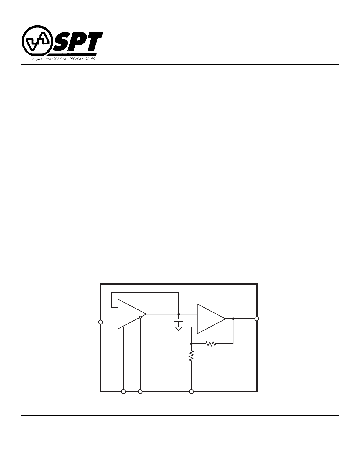
BLOCK DIAGRAM
Signal Processing Technologies, Inc.
Phone: (719) 528-2300 FAX: (719) 528-2370 Website: http://www.spt.com E-Mail: sales@spt.com
-
Sampler
V
In
+
CLK NCLK
4755 Forge Road, Colorado Springs, Colorado 80907, USA
C
H
OLD
R
RTN
+
Amp
-
4X
3R
V
UT
O
Page 2

ABSOLUTE MAXIMUM RATING (Beyond which damage may occur)
1
Supply Voltages
Supply Voltage (+VS) ................................-0.5 V to +6 V
Output Currents
Continuous Output Current ...................................70 mA
Supply Voltage (-VS)................................. -6 V to +0.5 V
Temperature
Input Voltages
Analog Input Voltage ................................................±5 V
CLK, NCLK Input .......................................-5 V to +0.5 V
Operating Temperature ..............................-40 to +85 °C
Junction Temperature ......................................... +150 °C
Lead, Soldering (10 seconds)............................. +220 °C
Storage .....................................................-65 to +150 °C
Note 1: Operation at any Absolute Maximum Ratings is not implied. See Electrical Specifications for proper nominal
applied conditions in typical application.
ELECTRICAL SPECIFICATIONS
+VS=+5.0 V, -VS=-5.2 V, R
PARAMETERS CONDITIONS LEVEL MIN TYP MAX UNITS
DC Performance
Gain ∆VIN = 0.5 V +25 °C I 3.93 4.0 4.07 V/V
Offset ∆VIN = 0 V +25 °CI ±3 ±10 mV
Output Resistance +25 °C V 0.5 Ω
Output Short Circuit Current Full Temp. V ±60 mA
PSRR ∆VS = 0.5 V p-p +25 °CVI3743dB
Pedestal Sensitivity to Pos. Supply Full Temp. V 4 mV/V
∆VS = 0.5 V p-p
Pedestal Sensitivity to Neg. Supply Full Temp. V 8 mV/V
∆VS = 0.5 V p-p
Analog Input/Output
Maximum Output Voltage Range6Full Temp. VI ±2.4 ±2.7 V
Input Bias Current +25 °CI ±15 ±30 µA
Input Capacitance +25 °CV 2pF
Input Resistance Full Temp. VI 100 450 kΩ
Clock Inputs
Input Bias Current +25 °CVI 330µA
Input Low Voltage Full Temp. VI -1.8 -1.5 V
Input High Voltage Full Temp. VI -1.0 -0.8 V
Track Mode Dynamics
Bandwidth (-3 dB) V
Slew Rate 4 V Output Step Full Temp. IV 1100 1400 V/µs
Overdrive Recovery Time
Integrated Output Noise BW = 5 to 200 MHz V 270 µV
Input RMS Spectral Noise 10 MHz V 3.9
=100 Ω, unless otherwise specified.
LOAD
TEST TEST SPT9101
Full Temp. VI 3.9 4.1 V/V
Full Temp. VI ±30 mV
Full Temp. VI ±35 µA
= 1.0 V p-p Full Temp. IV 150 180 MHz
Out
1
To 0.1% V 55 ns
nV
Hz
SPT
SPT9101
2 12/30/99
Page 3

ELECTRICAL SPECIFICATIONS
+VS=+5.0 V, -VS=-5.2 V, R
=100 Ω, unless otherwise specified.
LOAD
TEST TEST SPT9101
PARAMETERS CONDITIONS LEVEL MIN TYP MAX UNITS
Hold Mode Dynamics
Worst Harmonic 23 MHz, 50 MSPS V -75 dB FS
V
= 2 V p-p +25 °C
Out
Worst Harmonic 48 MHz, 100 MSPS IV -62 -57 dB FS
V
= 2 V p-p +25 °C
Out
Worst Harmonic 48 MHz, 100 MSPS IV -53 dB FS
V
= 2 V p-p Full Temp.
Out
Worst Harmonic 48 MHz, 125 MSPS V -57 dB FS
V
= 2 V p-p +25 °C
Out
Sampling Bandwidth
V
= 0.5 V p-p
IN
3
Hold Noise
(RMS) +25 °C V 150 x t
Droop Rate V
2
-3 dB, +25 ˚C V 350 MHz
H
=0.0 V, +25 °C V -40 mV/µs
IN
mV/s
Feedthrough Rejection (50 MHz) Full Temp. V -66 dB
V
= 2 V p-p
Out
Maximum Hold Time, VIN=0 V Full Temp. IV 100 200 ns
Track-and-Hold Switching
Aperture Delay +25 °C V -250 ps
Aperture Jitter +25 °C V <1 ps rms
Pedestal Offset, V
=0 V +25 °CI±10 ±25 mV
IN
Full Temp. VI ±35 mV
Transient Amplitude VIN = 0 V, Full Temp. V 8 mV
Settling Time to 4 mV Full Temp. V 4 ns
Glitch Product
4
+25 °C V 20 pV-s
VIN = 0 V
Hold-to-Track Switching
Acquisition Time to 0.1% +25 °CV7ns
2 V Output Step
Acquisition Time to 0.01% +25 °CIV1114ns
2 V Output Step Full Temp. IV 16 ns
Power Supply
5
+VS Voltage Full Temp, Track Mode VI 54 65 mA
Full Temp, Clocked Mode VI 44 55 mA
-V
Voltage Full Temp, Track Mode VI 54 65 mA
S
Full Temp, Clocked Mode VI 44 55 mA
Power Dissipation Full Temp, Track Mode VI 551 663 mW
Full Temp, Clocked Mode VI 449 561 mW
1
Time to recover within rated error band from 160% overdrive.
2
Sampling bandwidth is defined as the -3 dB frequency response of the input sampler to the hold capacitor when operating in the
sampling mode. It is greater than tracking bandwidth because it does not include the bandwidth of the output amplifier.
3
Hold mode noise is proportional to the length of time a signal is held. For example, if the hold time (tH) is 20 ns, the accumulated
noise is typically 3 µV (150 mV/s x 20 ns). This value must be combined with the track mode noise to obtain total noise.
4
Total energy of worst case track-to-hold or hold-to-track glitch.
Typical thermal impedances: ΘJC (LCC) = +6 °C/W
ΘJA (SOIC) = +85 °C/W in still air at +25 °C ambient.
5
Clocked mode is specified with a 50% clock duty cycle.
6
Analog input voltage should be limited ≤0.8 volts to maintain device in linear range.
SPT
3 12/30/99
SPT9101
Page 4

TEST LEVEL CODES
TEST LEVEL
TEST PROCEDURE
All electrical characteristics are subject to the
following conditions: All parameters having min/
max specifications are guaranteed. The Test
Level column indicates the specific device testing actually performed during production and
Quality Assurance inspection. Any blank section in the data column indicates that the specification is not tested at the specified condition.
Figure 1 - Timing Diagram
Input
Observed at
Hold Capacitor
III
IV
VI
Acquisition
Time
I
II
100% production tested at the specified temperature.
100% production tested at TA=25 °C, and sample
tested at the specified temperatures.
QA sample tested only at the specified temperatures.
Parameter is guaranteed (but not tested) by design
and characterization data.
V
Parameter is a typical value for information purposes
only.
100% production tested at TA = 25 °C. Parameter is
guaranteed over specified temperature range.
Aperature
Delay
Output
Amplifier Output
CLK
NCLK
Hold Track Hold
TIMING SPECIFICATION DEFINITIONS
ACQUISITION TIME
This is the time it takes the SPT9101 to acquire the analog
signal at the internal hold capacitor when it makes a transition
from hold mode to track mode. (See figure 1.) The acquisition
time is measured from the 50% input clock transition point to
the point when the signal is within a specified error band at the
internal hold capacitor (ahead of the output amplifier). It does
not include the delay and settling time of the output amplifier.
Because the signal is internally acquired and settled at the
hold capacitor before the output voltage has settled, the
sampler can be put in hold mode before the output has settled.
Observed at
Track-to-Hold
Settling
TRACK-TO-HOLD SETTLING TIME
The time required for the output to settle to within 4 mV of its
final value.
APERTURE DELAY
The aperture delay time is the interval between the leading
edge transition of the clock input and the instant when the
input signal was equal to the held value. It is the difference
in time between the digital hold switch delay and the analog
signal propagation time. Because the analog propagation
time is longer than the digital delay in the SPT9101, the
aperture delay is a negative value.
SPT
SPT9101
4 12/30/99
Page 5

Figure 2 - Typical Interface Circuit
+
2.2 µF
15 18
V
IN
CLK IN
3
X
4
V
t
V
+A5
2
V
CC
IN+
SPT, HCMP96850
IN-
LE
6
THEORY OF OPERATION
S
-V
IN
GND
1,16
-A5.2
8
V
EE
2.2 µF
+
+A5-A5.2
S
S
S
-V
-V
-V
458912 13 17 18
+V
SPT9101
10 11
-A5.2
11
12
330
220
330
220
S
S
-A5.2
S
+V
+V
V
OUT
6,7,161,2
V
OUT
S
+V
GNDRTN NCLKCLK
NOTES:
1) Vt = Threshold voltage:
a) For TTL or CMOS Clock input
+A5
b) For ECL Clock input
-A5.2
2) Unless otherwise specified, all capacitors
are 0.01 or 0.1 µF, surface mount.
3) X = Termination (if required).
4) CLKIN
a) TTL/CMOS
CLKIN
b) ECL: Direct Input
1k
3k
V
t
3k
1k
V
t
R
96850
R
CLOCK DRIVER CIRCUIT (CLK, NCLK PINS)
The SPT9101 is a monolithic 125 MSPS track and hold
amplifier built on a very high-speed complementary bipolar
process. It is pin and functionally compatible with the AD9101.
It is a two stage design with a sampler driving a hold capacitor
followed by a noninverting output buffer amplifier with gain of
4. The first stage sampler is based on a current amplifier in
noninverting gain of one configuration with inverting input
connected to the output. The hold switch is integrated into this
closed-loop first stage amplifier.
The output buffer amplifier is in a noninverting gain of 4
configuration with inverting input connected to a resistor
divider driven from the output. The noninverting input from the
hold capacitor employs input bias current cancellation which
results in excellent droop rate performance. The sampler and
amplifier stages both employ complementary current amplifiers for high-speed, low-distortion performance.
TYPICAL INTERFACE CIRCUIT
BOOTSTRAP CAPACITOR
The SPT9101 does not require the bootstrap capacitor that is
required on the AD9101 between pins 3 and 19. Because
pins 3 and 19 are No Connects on the SPT9101, it will work
well in existing AD9101 sockets.
SPT highly recommends that a differential ECL clock be used
to drive the SPT9101. Both the 10KH and 100KH family of
ECL logic can be used. The typical interface diagram, figure
2, shows the use of a SPT HCMP96850 high-speed comparator. The comparator has a typical propagation delay of
2.4 ns, very low offset of 3 mV, and a minimum tracking
bandwidth of 300 MHz. The comparator shown has been set
up in a feedthrough operation mode with latch enable connected to a logic high.
The threshold voltage (Vt) can be set using a resistor divider
as shown in note 1 of figure 2. The configuration shown in
note 1a is for a TTL/CMOS clock input and the configuration
shown in note 1b is for an ECL clock input. The differential
output of the comparator is directly fed to the SPT9101 clock
input. The comparator can also be driven with a sinewave
input, with the threshold voltage (Vt) adjusted to produce the
desired track/hold duty cycle ratio.
Note 4a shows the resistor divider configuration for a TTL/
CMOS clock input. If an ECL clock is used it can be directly
fed into the comparator.
OUTPUT LEVEL SHIFTING (RTN PIN)
The RTN pin is tied to the output buffer amplifier internal
feedback resistor network as shown in the block diagram.
Normally this pin is tied to ground for a 4x gain output amplifier
configuration. However, this pin may be configured in other
ways as long as certain guidelines are met.
SPT
SPT9101
5 12/30/99
Page 6

The RTN pin may be tied to an external voltage to generate
SPT9101 SPT7922
V
IN
Clock 1 Clock 2
12
0
an offset at the output. V
typical output swing. V
must be kept to less than ±2.7 V
Out
, with an external reference voltage
Out
at the RTN pin, is represented by the following formula:
V
= 4 VIN - 3 V
Out
where V
Ref
Ref
= voltage at RTN pin and | V
| ≤ 2.7 V
Out
The following options are generally not recommended due to
the possibility of degraded noise performance of the device:
the RTN pin can also be tied to an external resistor to reduce
the gain but performance may degrade due to increased
noise from the external resistor. Also RTN can be left open for
unity gain mode, however, noise will increase.
SAMPLER FOR 12-BIT ADC APPLICATION
The SPT9101 was specifically designed for applications
where improved bandwidth performance is required. Figure 3
shows as simple block diagram of the SPT9101 as a sampler
ahead of our SPT7922 12-bit, 30 MSPS ADC.
Figure 3 - Sampler for 12-Bit ADC
In all cases, VIN must be kept to -0.5 V≤ V
performance.
PERFORMANCE CHARACTERISTICS
Droop Rate vs Temperature
40
0
-40
mV/us
-80
-120
-20020406080
Temperature (°C)
≤ +0.5 V for rated
IN
The graph below entitled Improved Dynamic Performance
Using the SPT9101 shows the performance with and without
the SPT9101. The SPT9101 significantly extends the dynamic performance range of the converter.
SPT9101 Hold Mode Distortion vs. Temperature
-65
Input Frequency = 50 MHz
Clock Frequency = 100 MHz
Hold = 4 ns
Track = 6 ns
dB
Worst Harmonic
-60
-50 -25 0 25 50 75 10
Temperature (°C)
SPT9101 Hold Mode Distortion vs Input Frequency
-75
-70
-65
dB
Clock Frequency = 100 MHz
Track = 6 ns
-60
Hold = 4 ns
-55
1 10 100
Input Frequency (MHz)
SPT
Worst Harmonic
6 12/30/99
Improved Dynamic Performance Using the SPT9101
70
SPT9101 & SPT7922
60
TDE (dB)
50
(FS = 28 MSPS)
40
5101520
SPT7922
FIN (MHz)
SPT9101
Page 7

PACKAGE OUTLINES
20-Lead LCC
A
H
SYMBOL MIN MAX MIN MAX
G
Bottom
B
C
View
Pin 1
F
INCHES MILLIMETERS
A .040 typ 1.02
B .050 typ 1.27
C 0.045 0.055 1.14 1.40
D 0.345 0.360 8.76 9.14
E 0.054 0.066 1.37 1.68
F .020 typ 0.51
G 0.022 0.028 0.56 0.71
H 0.075 1.91
D
E
F
20
1
C
DE
A B
G
20-Lead SOIC
H
INCHES MILLIMETERS
SYMBOL MIN MAX MIN MAX
A 0.291 0.299 7.40 7.60
B 0.394 0.419 10.00 10.65
C 0.496 0.512 12.60 13.00
D 0.050 typ 1.27 typ
E 0.014 0.019 0.35 0.49
F 0.004 0.012 0.10 0.30
G 0.093 0.104 2.35 2.65
H 0.009 0.013 0.23 0.32
I 0.016 . 0.050 0.40 1.27
I
SPT
SPT9101
7 12/30/99
Page 8

PIN ASSIGNMENTS
1
RTN
2
RTN
3
N/C
4
+V
S
5
+V
S
GND
GND
6
7
SOIC
20
19
18
17
16
15
14
V
Out
N/C
-V
S
-V
S
GND
V
In
N/C
PIN FUNCTIONS
Name I/O Function
RTN I Gain Set Resistor Return
+V
S
GND I Ground
CLK I True ECL T/H Clock
NCLK I Complement ECL T/H Clock
-V
S
N/C - No Connection
V
IN
V
OUT
I +5 V Power Supply
I -5.2 V Power Supply
I Analog Signal Input
O Analog Signal Output
+V
S
N/C
3
9
13
-V
S
12
-V
S
11
NCLK
4
+V
S
5
+V
S
GND
6
GND
7
8
+V
S
+V
+V
CLK
-V
-V
GND
V
IN
N/C
8
S
9
S
10
V
RTN
1
LCC
11
NCLK
RTN
2
10
CLK
N/C
Out
19
20
18
S
17
S
16
(Bottom View)
15
14
13
12
-V
-V
S
S
ORDERING INFORMATION
PART NUMBER PACKAGE TYPE TEMPERATURE RANGE
SPT9101SIS 20L SOIC -40 to +85 °C
SPT9101SIC 20L LCC -40 to +85 °C
SPT9101SCU Die* +25 °C
*Please see die specification for guranteed electrical performance.
Signal Processing Technologies, Inc. reserves the right to change products and specifications without notice. Permission is hereby expressly
granted to copy this literature for informational purposes only. Copying this material for any other use is strictly prohibited.
WARNING - LIFE SUPPORT APPLICATIONS POLICY - SPT products should not be used within Life Support Systems without the specific
written consent of SPT. A Life Support System is a product or system intended to support or sustain life which, if it fails, can be reasonably
expected to result in significant personal injury or death.
Signal Processing Technologies believes that ultrasonic cleaning of its products may damage the wire bonding, leading to device
failure. It is therefore not recommended, and exposure of a device to such a process will void the product warranty.
SPT9101
SPT
8 12/30/99
 Loading...