

Page 1
FEATURES
SPT8100
16-BIT, 5 MSPS CMOS A/D CONVERTER
TECHNICAL DATA
JANUARY 9, 2002
APPLICATIONS
• 16-bit, 5 MSPS CMOS analog-to-digital converter
• On-chip PGA: gain range from 0 to 19.5 dB in se v e n
selectable settings:
0 dB, +2.9 dB, +5.8 dB, +11.8 dB , +14.8 dB , +17.5 dB ,
+19.5 dB
• DLE: ±0.5 LSB , ILE: ±1.25 LSB
• SFDR: 94 dB @ ƒIN = 900 kHz, –8.1 dBFS
• Internal sample-and-hold and voltage reference
• Po wer dissipation: 465 mW at 5 MSPS
• +5 V analog supply and +3.3 to +5.25 V digital output
supply
• 44-lead LQFP plastic package
DESCRIPTION
The SPT8100 is a high-performance, 16-bit analog-todigital converter that operates at a sample rate of up to
5 MSPS. Excellent dynamic performance and high linearity is achieved by a digitally calibrated pipelined architecture fabricated in CMOS process technology.
A low-noise programmable gain amplifier (PGA) is also incorporated on chip. The PGA is digitally programmable in
seven selected settings over a 0 to +19.5 dB range. The
• Data acquisition systems
• IR imaging
• Scanners and digital copiers
• High-end CCD cameras
• Medical imaging
• Wireless communications
• Lab and test equipment
• Automatic test equipment
SPT8100 also features an on-chip internal sample-andhold and internal reference for minimal e xternal circuitry .
It operates from a single +5 V supply. Total power dissipation, including internal reference, is 465 mW. A separate
digital output supply pin is provided for +3.3 V or 5 V logic
output levels. The SPT8100 is available in a 44-lead LQFP
package over the industrial temperature range of –40 °C to
+85 °C.
BLOCK DIAGRAM
V
+
IN
V
–
IN
V
CM
GS2 – GS0
(Gain Set)
Low-Noise
AGND
PGA
DD
DV
+5V
AV
+5V
16-bit, 5 MSPS ADC
VREF
OGNDDGND
BIAS
C
(Ext Bias
Capacitor)
BIAS
(Ext Bias
Resistor)
V
R
RTVRB
DD
OV
DD
+3/5 V
CLK
16-bits
OE (Output Enable)
OVR (Over-Range)
D15 – D0
(Data Outputs)
RS (Reset)
RDY (Ready)
Page 2

ABSOLUTE MAXIMUM RATINGS (Beyond which damage may occur)1 25 °C
Supply V oltages
AVDD...................................................................... +6 V
DVDD..................................................................... +6 V
OVDD..................................................................... +6 V
Input V oltages
Analog Input ................................. –0.5 V to VDD +0.5 V
CLK Input ............................................................... V
AVDD – DVDD.................................................. ±100 mV
Delta between AGND, DGND , and OGND...... ±100 mV
Output
Digital Outputs.................................................... 10 mA
T emperature
Operating T emperature........................... –40 to +85 °C
Junction T emperature ...................................... +175 °C
Lead Temperature (soldering 10 seconds) ...... +300 °C
DD
Storage T emperature............................ –65 to +150 °C
Note 1: Operation at any Absolute Maximum Rating is not implied. See
Electrical Specifications for proper nominal applied conditions in
typical applications.
ELECTRICAL SPECIFICATIONS
TA=T
otherwise specified.
PARAMETERS CONDITIONS LEVEL MIN TYP MAX UNITS
Resolution 15.9 16 Bits
DC Accuracy
Analog Input (into PGA)
MIN
to T
, AVDD=DVDD=+5.0 V, OVDD= 3.3 V, ƒS=5 MSPS, 2.5 VPP input span, Gain=0 dB, R
MAX
=1.43 kΩ, unless
EXT
TEST TEST SPT8100
Integral Linearity Error (ILE) V ±1.25 LSB
Differential Linearity Error (DLE) V ±0.5 LSB
Gain Error
Offset Error
1
2
IV –7.5 +7.5 %FSR
IV –5+5%FSR
Differential Input Voltage Range
+, VIN– V5V
V
IN
PPD
Input Capacitance IV 15 pF
Input Resistance
Input Bandwidth
3
4
PGA Gain = 0 dB IV 5.5 kΩ
PGA Gain = 0 dB V 12 MHz
Input Common Mode Voltage Range V 1.15 2.40 3.65 V
Programmable Gain Amp
Composite Input-Referred ƒ
> 300 kHz
IN
Noise Floor PGA Gain = 0 dB V 1.4 LSB
PGA Gain = 2.9 dB V 1.5 LSB
PGA Gain = 5.8 dB V 1.6 LSB
PGA Gain = 11.8 dB V 2.0 LSB
PGA Gain = 14.8 dB V 2.3 LSB
PGA Gain = 17.5 dB V 2.6 LSB
PGA Gain = 19.5 dB V 2.8 LSB
PGA Range V 19.5 dB
PGA Gain Steps
3
VI 0,2.9,5.8,11.8,14.8,17.5,19.5 dB
PGA Gain Accuracy VI ±0.3 dB
Conversion Characteristics
Maximum Conversion Rate VI 5 MSPS
Pipeline Delay (Latency)
Reset Pulse Time (
RS) IV 3 Clocks
5
IV 5.5 Clocks
Reset Calibration Time FS = 5 MSPS V 150 ms
References and External Bias
– VRB (Internal Ref) VI 2.375 2.5 2.625 V
V
RT
Bias Resistor Range (External) V 800 1430 2500 Ω
Output Voltage IV 2.275 2.40 2.525 V
V
CM
Output Current IV 47 µA
V
CM
V
RT
V
RB
1
Total gain error of PGA and ADC using inter nal references.
2
Total offset error of PGA and ADC relative to mid-scale.
3
See table I for input resistance as a function of PGA gain.
4
Input bandwidth is a frequency to which the fundamental energy drops by 3 dB
5
The input is sampled on the falling edge of the clock and is available on the
output after the rising edge of the clock, 5.5 clock cycles later.
V 3.45 3.65 3.85 V
V 0.95 1.15 1.35 V
RMS
RMS
RMS
RMS
RMS
RMS
RMS
SPT8100
2 1/9/02
Page 3

ELECTRICAL SPECIFICATIONS
TA=T
otherwise specified.
PARAMETERS CONDITIONS LEVEL MIN TYP MAX UNITS
Dynamic Performance
MIN
to T
, AVDD=DVDD=+5.0 V, OVDD= 3.3 V, ƒS=5 MSPS, 2.5 VPP input span, Gain=0 dB, R
MAX
=1.43 kΩ, unless
EXT
TEST TEST SPT8100
1
Effective Number of Bits ADC Input = –1 dBFS
2
ƒIN = 60 kHz IV 12.2 13.0 Bits
= 900 kHz V 12.7 Bits
ƒ
IN
Signal-to-Noise Ratio
(without Harmonics) ADC Input = –1 dBFS
2
ƒIN = 75 kHz IV 78 81 dB
ƒ
= 900 kHz V 80 dB
IN
Harmonic Distortion ADC Input = –0.5 dBFS
= 60 kHz IV –92 –84 dB
ƒ
IN
ƒ
= 900 kHz V –82 dB
IN
Signal-to-Noise and Distortion
(SINAD) ADC Input = –1 dBFS
= 60 kHz IV 75 80 dB
ƒ
IN
= 900 kHz V 78 dB
ƒ
IN
Spurious Free Dynamic Range
3
ƒIN = 60 kHz ADC Input = –0.5 dB IV 85 94 dBc
= 900 kHz V 94 dBc
ƒ
IN
= 2 MHz R
ƒ
IN
ƒIN = 3 MHz R
= 1 kΩ @ 10 MSPS V 83 dBc
EXT
= 1 kΩ @ 10 MSPS V 78 dBc
EXT
Two-Tone Intermodulation
3rd Order Distortion ƒ
=400 kHz, ƒ2=410 kHz
1
ƒ1=890 kHz, ƒ2=900 kHz
4
V –94 dB
5
V –89 dB
Inputs
GS0–GS2 Logic 1 Voltage VI 2.4 V
GS0–GS2 Logic 0 Voltage VI 0.8 V
RS Logic 1 Voltage VI 2.0 V
CLK,
RS Logic 0 Voltage VI 0.8 V
CLK,
Maximum Input Current Low VI –10 +10 µA
Maximum Input Current High VI –10 +10 µA
Input Capacitance V 5 pF
Digital Outputs
Logic 1 Voltage I
= –2 mA VI OVDD – 0.5 V
OH
Logic 0 Voltage IOL = 2 mA VI 0.4 V
CLK to Output Delay Time (t
)C
D
= 20 pF IV 30 ns
LOAD
Power Supply Requirements
Voltages OV
AV
DV
Currents I
DD
DD
DD
DD
IV 3.0 3.3 5.25 V
IV 4.75 5.0 5.25 V
IV 4.75 5.0 5.25 V
VI 93 103 mA
Power Dissipation VI 4 65 515 mW
1
Dynamic performance tested at ƒS=4.4 MSPS
2
0 dBFS is 5.0 V peak-to-peak differential
3
ADC Input = –8.1 dBFS, unless otherwise noted
TEST LEVEL CODES
All electrical characteristics are subject
to the following conditions:
All parameters having min/max specifications are guaranteed. The Test Level
column indicates the specific device
testing actually performed during
production and Quality Assurance
inspection. Any blank section in the data
column indicates that the specification is
not tested at the specified condition.
TEST LEVEL TEST PROCEDURE
I 100% production tested at the specified temperature.
II 100% production tested at TA = +25 °C, and sample tested at the
III QA sample tested only at the specified temperatures.
IV Parameter is guaranteed (but not tested) by design and characteriza-
V Parameter is a typical value for information pur poses only.
VI 100% production tested at TA = +25 °C. Parameter is guaranteed
4
Test Conditions: PGA setting of 5.8 dB; Analog Input at ADC = –0.7 dB
5
Test Conditions: PGA setting of 0 dB; Analog Input at ADC = –1.9 dB
specified temperatures.
tion data.
over specified temperature range.
SPT8100
3 1/9/02
Page 4

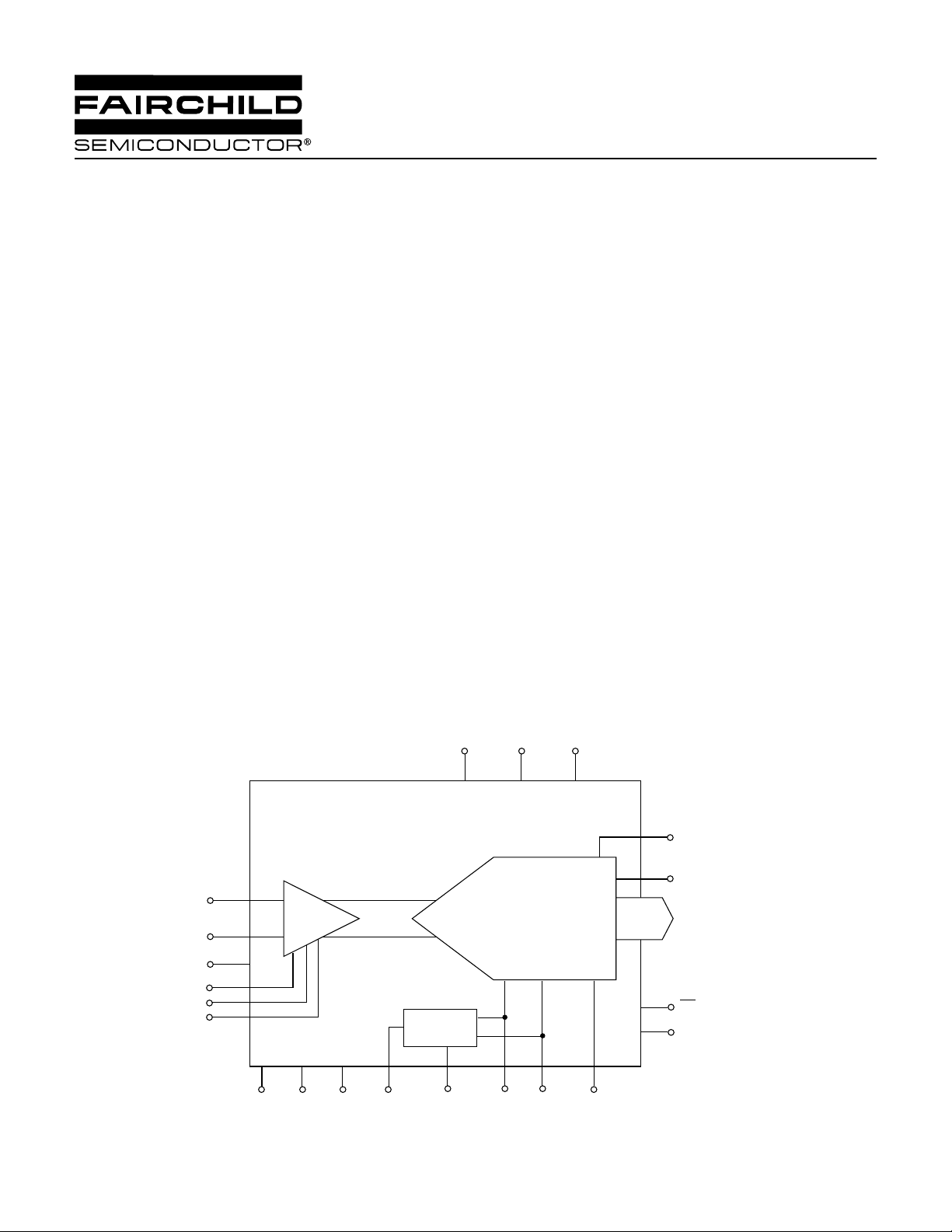
DEVICE OVERVIEW
ADC CLOCK
The SPT8100 combines a high-resolution 5 MSPS 16-bit
ADC, a built-in reference, and a programmable gain amplifier (PGA) with resistive input impedance in a 44-pin
package.
The device includes a digitally calibrated pipeline ADC,
which is calibrated on assertion of a simple reset signal.
The combination of low noise, high linearity, a high-input
impedance buffer (with programmable gain), wideband
S/H, on-board voltage references , and simple digital interface (16-bit parallel output word synchronous with the
master sampling clock) makes the SPT8100 extremely
easy to use in a wide variety of systems.
For optimum performance, the analog inputs should be
driven differentially, and may be AC-coupled or DCcoupled to a source. Typical applications include high-performance data acquisition systems, automatic test equipment, and wideband digital communications receivers
such as wireless basestations.
OPERATIONAL DESCRIPTION
The following sections describe in greater detail individual
blocks and functions of the SPT8100.
The incoming analog differential signal (maximum le vel 5 V
peak-to-peak differential) enters the device at the pins
VIN+/VIN–. The analog signal path is partitioned into a programmable gain amplifier (PGA) and an ADC. The PGA
has maximum gain of +19.5 dB; the gain is set b y the digital control signals GS0 to GS2.
The output of the PGA is fed directly to the ADC, which
samples at a rate equal to the CLK frequency and outputs
a 16-bit wide parallel word. The ADC uses a pipeline multistage architecture. Latency is 5.5 cloc k cycles .
The chip requires a single low-jitter clock to be applied at
the CLK pin, with nominal 40–60% duty cycle. All clock
generation is performed internally and all converter and
S/H clocks in the ADC path are directly derived from CLK.
If the sample rate is changed by more than a factor of 2,
the device must be recalibrated using the RS (reset) pin.
DEVICE ST ARTUP/INITIALIZATION SEQUENCE
Note: This initialization sequence is
required
. Without
it, the device will not work.
Allow sufficient time for the analog bloc ks on the SPT8100
to power on and come up to their quiescent DC states.
Allowance may also be needed f or thermal time constants
associated with the package/board.
On powerup, the SPT8100’s RS (reset) should be held low
for at least three clock cycles. The power supply voltages
applied to the device must be stable during this time. The
clock signal (CLK) must be running for at least three cloc k
cycles prior to the rising edge of RS, and must continue
running.
When the RS signal goes from low to high, calibration is initiated. RDY is driven low two clock cycles after the rising
edge of RS, and will stay low for 150 ms with a 5 MHz cloc k.
When the initialization is complete, RDY returns high and
the device is ready for normal operation. Note that the calibration of the ADC can be interrupted (before completion)
by changing the RS signal from high to low, which will
cause another reset to occur. When RS goes from low back
to high, another calibration cycle will begin.
RDY cannot be tri-stated: it is alwa ys driven either high or
low. The CLK must be constantly running throughout the
Figure 1 – Device Initialization Timing
PWR ON
A
IN
CLK
RS
RDY
D
OUT
Requires external reset on powerup
3 clock cycles min
N+8
N+7
N+4
2 clock cycles
Initialization period: 150 ms with 5 MHz clock
INVALID DATA
N+6
N+5
5 ns typ
24 ns typ
N N+1 N+2
SPT8100
4 1/9/02
Page 5

initialization phase until RDY is deasserted. Note that,
although typically the device is initialized when power is
first applied, the initialization is only started when the
RS is
asserted; there is no “power-on-reset” circuitry on chip. RS
may be held low f or an indefinite period of time. While RS is
low , RD Y will remain high. After RS is returned to high, RDY
will go low for the duration of the calibration.
PROGRAMMABLE GAIN AMPLIFIER
The programmable gain amplifier (PGA) precedes the
ADC inputs. The diff erential inputs, which are resistive , are
at pins VIN+ and VIN–.The maximum input range is 5 V
peak-to-peak differential (2.5 V single-ended). To achieve
maximum overall system noise performance, the source
driving these inputs needs to be as low-noise and as lowjitter as possible, while maintaining the required distortion
performance. In addition, the driving source must be low
impedance to maintain the accuracy of the PGA gain.
TYPICAL INTERFACE CIRCUIT
ANALOG INPUT DRIVER
The differential analog inputs (VIN+, VIN–) have a resistiv e
input impedance of 1 kΩ minimum. F or best perf ormance,
the input source should be a differential input, as shown in
figure 2, typical interface circuit. The SPT8100 provides its
own common-mode voltage on the pin marked V
put drive capability of VCM is a maximum of 47 µA (50 kΩ to
ground).
The SPT8100 application note (AN8100) shows an example of two modes of driving the SPT8100. One mode is
through a transformer and the other is through a single-todifferential conver ter. In all cases, both inputs VIN+ and
VIN– must be kept within the input common-mode range
(1.15 V to 3.65 V).
BIASC CONNECTION
CM
. Out-
The internal 0 dB analog signal level and ADC full-scale
output level is 5 V peak-to-peak differential (2.5 V singleended). The PGA ma y be used to provide gain f or an input
less than 5 V peak-to-peak diff erential.
The gain of the PGA can be programmed using a three-bit
control, availab le at pins GS0 to GS2. See tab le I. Note that
the input resistance is a function of the gain setting.
Table I – PGA Gain Control
GS2 GS1 GS0 Gain Resistance Gain BW LSB
0 0 0 0 5.57 1 12 1.4
0 0 1 2.9 4.65 1.40 10 1.5
0 1 0 5.8 3.97 1.95 8 1.6
0 1 1 11.8 2.23 3.9 7 2.0
1 0 0 14.8 1.66 5.5 6 2.3
1 0 1 17.5 1.25 7.5 5.5 2.6
1 1 0 19.5 1.00 9.5 5 2.8
1 1 1 X Forbidden
PGA Input V/V 3 dB
(dB) (k
ΩΩ
Ω)
ΩΩ
RMS
An external capacitor, C
on the BIASC pin, is used only
EXT
for noise filtering of an internal voltage associated with the
references. Its value is not critical: 1 µF in parallel with
0.01 µF is recommended.
BIASR CONNECTION
As shown in the typical interface circuit, R
is needed to
EXT
connect between BIASR to ground. This resistor ranges
from 800 Ω to 2.5 kΩ. The proper selection of R
EXT
is a
function of the sample rate and input frequency . Nominally ,
at 5 MSPS, R
=1.43 kΩ is recommended. If linearity for
EXT
large signal levels at an analog bandwidth of 2 MHz is critical, the value should be decreased to R
for ev en higher-frequency analog inputs, R
=1.24 kΩ; and
EXT
=1.0 kΩ can
EXT
be used. At lower sample rates (for example 2 MSPS),
and lower analog input frequencies, the value may be increased to R
=2 kΩ. (Ref er to the typical interface circuit
EXT
table in figure 2b.)
POWER SUPPLIES AND GROUNDING
The SPT8100 requires three power supplies: analog A VDD,
digital DVDD and output supply OVDD. This device works
best if all three supplies are coming from the analog supply
side of the system as shown in the typical interface circuit
(figure 2a).
Note, in figure 2a, that the supplies to the logic interface
circuit and the OVDD are separate from each other. In a
case where the +A3.3/5 V supply is not available, try to
implement the design as close as possible to that shown
in figure 2b. Place the ferrite bead (FB1) as close to the
device as possible. To avoid latch-up, the delta between
all three grounds must stay with 100 mV; this includes
transients. (Refer to the absolute maximum ratings
specifications.)
SPT8100
5 1/9/02
Page 6

Figure 2a – Typical Interface Circuit
A
IN
Transformer
Mini-Circuit
T1-6T
0.1
+
4.7
R
T
(50)
+
10 0.1 1nF
1.43K
R
EXT
VIN+
V
GS0
Output
Enable
(active Hi)
OE
Clock
Input
CLK
RDY
D0–15
OVR
DD
16
Logic
Interfacing
Circuit
1.0
+
.01
BIAS
BIAS
R
V
CM
Reset
C
RS
Gain Control
GS1
GS2
SPT8100
–
IN
V
RT
V
RB
AV
DD
AGND DGND OGND OV
DV
DD
Figure 2b – Typical Interface Circuit
A
IN
ƒS (MSPS) R
–5 1.43 <2 MHz
–2 2.00 <2 MHz
–5 1.24 •2 MHz
–2 1.00 •2 MHz
800 Ω – R
Transformer
Mini-Circuit
EXT
– 2.5 kΩ
EXT
T1-6T
(k
0.1
ΩΩ
Ω) ƒ
ΩΩ
+
4.7
IN
R
T
(50)
+
10 0.1 1nF
1.43K
R
EXT
VIN+
V
IN
0.1
10
+
+A5V +A3.3/5V
1.0
+
.01
BIAS
C
BIAS
R
V
CM
–
V
RT
V
RB
AV
DD
Gain Control
Reset
GS0
GS2
GS1
RS
SPT8100
AGND DGND OGND OV
DV
DD
0.1
10
+
FB1
0.1
10
+
FB1
Output
Enable
(active Hi)
OE
0.1
10
Clock
Input
CLK
RDY
D0–15
OVR
DD
+
FB2
FB3
+D3.3/5V
16
Logic
Interfacing
Circuit
+A5V +D3.3/5V
Notes:
1. To avoid device latch-up, closely follow either figure 2a or 2b, depending on what is available in the system. The difference between figure 2a
and 2b is in the grounding.
2. FB = ferrite bead. FB1 must be placed as close to the device as possible.
3. R
= 1.43 kΩ, optimized for ƒS = 5 MSPS. Refer to the above table for recommended value of R
EXT
with respect to ƒS and ƒIN.
EXT
4. RT is AIN source termination resistor.
5. Power supplies and references pins must have adequate decoupling. Surface-mount capacitors are highly recommended. The smallest value
of capacitors are to be placed as close to the pin as possible.
SPT8100
6 1/9/02
Page 7

Figure 3 – Timing Diagram 1
n
Analog In
CLK
t
D
D0D15
OVR
n+1
n+2
n+3
n+4
n+5
n+6 n+7
n
n+1
n+8
n+2
INPUT/OUTPUT TIMING
The SPT8100 implements a simple interface: the 16 ADC
outputs appear on the pins D15–D0 as a parallel word synchronous with the ADC sampling clock. D0 is the LSB and
D15 is the MSB. The timing diagram for the ADC digital
outputs is shown in figure 3. The data is sampled at the f alling edge of the clock. The ADC sampling clock is at the
same frequency as CLK.
The output data is updated on the rising edge of CLK with
a clock latency of 5.5 clock cycles.
OUTPUT LOGIC LEVEL
The voltage levels on the D15–D0 lines and OVR are
CMOS levels: the HIGH level is determined by the power
supply voltage on the O VDD pin, which can be set independently of the other supply pins on the device over the range
from 3.0 V to 5.25 V (3.3 V typical). The RDY pin level is
determined by DVDD (+5 V).The external digital output
buffers should be placed as close as possible to the
SPT8100 digital outputs to minimize any line reflections
that would cause performance degradation.
ADC REFERENCES
The ADC full-scale range is set by ref erence voltages generated on chip. These two reference voltages appear on
pins VRT and VRB; nominally their difference is 2.5 V. The
references are not designed to be ov erdriven. The VRT and
VRB pins should be very carefully decoupled on the board
using as short a trace as possible. Some optimization of
the decoupling may be required, as shown in the typical
interface circuit diagram. The smallest capacitor should be
the closest one to the chip. (Refer to the typical interface
circuit diagram.)
OUTPUT ENABLE
The ADC digital outputs are enabled by the active high
output enable pin (OE).
OE = 1: ADC digital outputs are enabled
OE = 0:ADC digital outputs are high-impedance
(tri-stated)
DIGITAL CODE RANGE AND
OUT-OF-RANGE DETECTION
The output format of the ADC digital data is offset binary.
Due to the calibration algorithm used, there is a slight loss
in digital code range from the ADC. Instead of FFFFH and
0000H at the extremes of the range, the actual maximum
and minimum codes are less than that by 1.6% at both
ends of the scale, and vary from chip to chip. Effectively,
this is a loss in dynamic range of a few tenths of a dB , and
is negligible in many applications. The out-of-range function is defined accordingly , and sets the state of the activ e
high digital output OVR, as f ollo ws:
OVR is HIGH if the ADC digital code is greater
than or equal to FC00H or less than or equal to
03FFH. (See figure 4.)
If the output code exceeds FC00(max) or 03FF(min), this
implies that output is clipping. Therefore, once these limits
are crossed, the second harmonic becomes significant
and degrades performance.
Figure 4 – ADC Digital Code Range and Overrange
Bit Function
FFFFH
FC00H
ADC
Digital Code
Range
OVR = 1
OVR = Ø
65535
64512
1.6% FSR
03FFH
0000H
OVR = 1
1023
0
1.6% FSR
SPT8100
7 1/9/02
Page 8

Figure 5 – Timing Diagram 2
CLK
Digital
Outputs
OE
t
D1
FFT Plot Typical Differential Linearity Error (DLE)
T ab le II – Timing Parameters
Parameter Symbol Min Typ Max Units
CLK high to Data Valid t
OE inactive to HiZ t
OE active to Data Valid t
1
Conditions: load capacitance = 20 pF, VOH = 3.3 V
t
D2
t
D3
DLE (LSB)
D1
D2
D3
18 24 40
10 16 30 ns
10 16 30 ns
1
ns
Test Conditions:
= 2 MHz
ƒ
IN
= 4.4 MHz
ƒ
CLK
PGA Gain = 18 dB
T wo-Tone Intermodulation FFT Spurious-Free Dynamic Range
Test Conditions:
= 890 kHz
ƒ
1
ƒ2 = 900 kHz
= 4.4 MHz
ƒ
CLK
PGA Gain = 6 dB
R
= 1.08 kΩ
EXT
ADC Input (Post PGA) = –5.4 dBFS
= +25 °C
T
A
= 1.43 kΩ
R
EXT
ADC Input (Post PGA) = –8.0 dBFS
= +25 °C
T
A
Test Conditions:
ƒIN = 75 kHz
= 4.4 MHz
ƒ
CLK
100
0.9 MHz, low
95
0.9 MHz, med
0.9 MHz, high
90
85
80
75
70
SFDR (dBc)
65
60
55
50
45
–9
–10
Composite Level at ADC Input (dBFS)
Test Conditions:
10 MSPS, 5 V, 25 °C
Low: R
=1.43 kΩ @96 mA
EXT
–8
PGA Gain = 0 dB
Near Full-Scale Input
–5
–6
–7
Med: R
High: R
2 MHz, high
2 MHz, med
2 MHz, low
3 MHz, high
3 MHz, med
3 MHz, low
–4
–3
–2
=1.24 kΩ @109 mA
EXT
=1 kΩ @129 mA
EXT
–1
5 V
0
P-P
SPT8100
8 1/9/02
Page 9

PACKAGE OUTLINE
44-Lead LQFP
A
B
SYMBOL MIN MAX MIN MAX
INCHES MILLIMETERS
A 0.465 0.480 11.80 12.20
B 0.390 0.398 9.90 10.10
Pin 1
Index
C 0.390 0.398 9.90 10.10
D 0.465 0.480 11.80 12.20
E 0.0315 BSC 0.80 BSC
F 0.012 0.018 0.30 0.45
C
D
G 0.053 0.057 1.35 1.45
H 0.002 0.006 0.05 0.15
I 0.018 0.030 0.45 0.75
J 0.039 typ 1.0 typ
K0–7° 0–7°
E F
G
H
I
K
J
SPT8100
9 1/9/02
Page 10

PIN ASSIGNMENTS PIN FUNCTIONS
AGND
DGND
DV
DV
OGND
OV
CLK
D0 (LSB)
OE
AV
DD
44
1
2
DD
3
4
DD
5
6
DD
7
8
9
D1
10
D2
11
12
D3
GS0
43
13
D4
V
IN
42
14
D5
V
IN
+
41
15
D6D7D8
V
GS1
CM
40
39
161718
AGND
38
D9
RT
V
37
19
D10
V
RB
36
20
D11
BIASRBIAS
C
35
34
21
22
D12
D13
Pin Name Description
AGND Analog ground
DGND Digital ground
RDY
33
N/C
32
31
N/C
RS
30
AGND
29
AV
28
DD
GS2
27
N/C
26
OVR
25
24
D15 (MSB)
23
D14
DV
DD
Digital +5.0 V supply
OGND Ground for digital I/O
OV
DD
Digital outputs supply (+3.3/5 V)
CLK Master reference clock
OE Output enable (active high)
D0–D15 Data output bits; D0 is LSB; D15 is MSB
OVR Overrange indicator bit (active high)
N/C No connect
GS[2:0] 3-bit PGA gain setting control inputs
AV
DD
RS Resets internal state of chip (active low)
Analog +5.0 V supply
RDY Initialization in progress indicator; RDY goes low
during reset initialization. Chip is ready for normal
operation when RDY is high.
BIAS
BIAS
VRT, V
V
CM
External bias capacitor connection
C
External bias resistor connection
R
ADC reference voltage outputs
RB
Common mode reference voltage output
VIN+, VIN– Analog inputs to the PGA
ORDERING INFORMATION
PART NUMBER TEMPERA TURE RANGE PACKAGE
SPT8100SIT –40 to +85 °C 44L LQFP
DISCLAIMER
FAIRCHILD SEMICONDUCTOR RESERVES THE RIGHT TO MAKE CHANGES WITHOUT FURTHER NOTICE TO ANY PRODUCTS HEREIN TO
IMPROVE RELIABILITY, FUNCTION OR DESIGN. FAIRCHILD DOES NOT ASSUME ANY LIABILITY ARISING OUT OF THE APPLICATION OR
USE OF ANY PRODUCT OR CIRCUIT DESCRIBED HEREIN; NEITHER DOES IT CONVEY ANY LICENSE UNDER ITS PATENT RIGHTS, NOR
THE RIGHTS OF OTHERS.
LIFE SUPPORT POLICY
FAIRCHILD'S PRODUCTS ARE NOT AUTHORIZED FOR USE AS CRITICAL COMPONENTS IN LIFE SUPPORT DEVICES OR SYSTEMS
WITHOUT THE EXPRESS WRITTEN APPROVAL OF THE PRESIDENT OF FAIRCHILD SEMICONDUCTOR CORPORATION. As used herein:
1. Life support devices or systems are devices or systems which, (a) are
intended for surgical implant into the body, or (b) support or sustain life,
and whose failure to perform, when properly used in accordance with
instructions for use provided in the labeling, can be reasonably
expected to result in a significant injury to the user.
www.fairchildsemi.com © Copyright 2002 Fairchild Semiconductor Corporation
2. A critical component is any component of a life support device or
system whose failure to perform can be reasonably expected to cause
the failure of the life support device or system, or to affect its safety or
effectiveness.
SPT8100
10 1/9/02
 Loading...