

Page 1
SPT7936
12-BIT, 28 MSPS SAMPLING A/D CONVERTER
FEATURES
• 3.0-3.6 V Power Supply
• Typical SINAD: 60 dB for (f
= 10 MHz)
IN
• Low power: (260 mW @3.3 V)
• Sample Rate: 28 MSPS
• Internal Sample/Hold
• Differential Input
• Sleep Mode (Power Down)
GENERAL DESCRIPTION
The SPT7936 is a compact, high-speed, low power 12-bit
monolithic analog-to-digital converter, implemented in a
0.5 µm CMOS process. The converter includes sample and
hold. The full scale range can be set between ±0.6 V and ±1.2
V using external references. It operates from a single 3.0-3.6
V supply-compatible with modern digital systems. Most converters in this performance range demand at least a +5 V
supply. Its low distortion and high dynamic range offers the
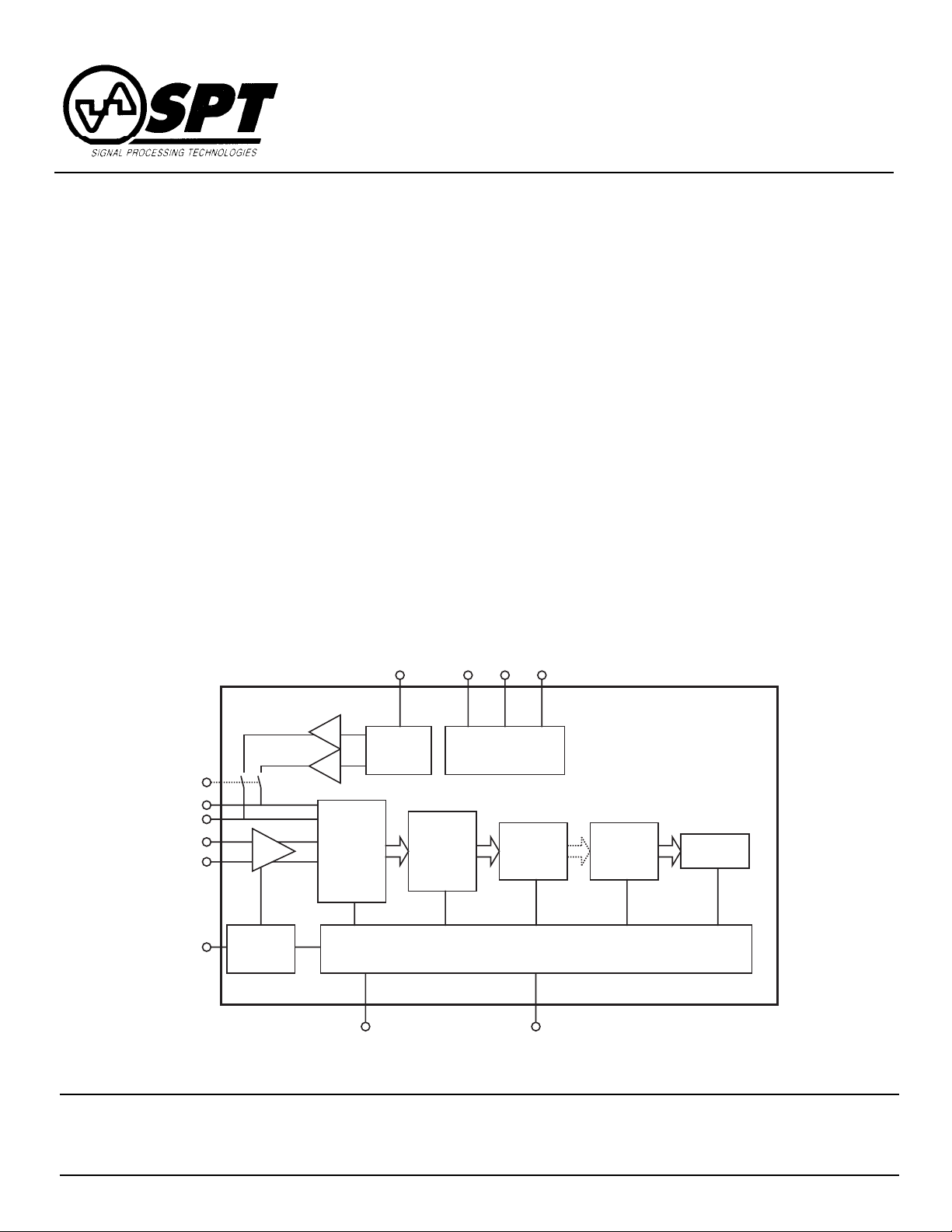
BLOCK DIAGRAM
BGAP
APPLICATIONS
• Imaging
• Test Equipment
• Computer Scanners
• Communications
• Set-Top Boxes
performance needed for demanding imaging, multimedia,
telecommunications and instrumentation applications.
The SPT7936 has a pipelined architecture - resulting in low
input capacitance. Digital error correction of the 11 most
significant bits ensures good linearity for input frequencies
approaching Nyquist.
The device is available in a 44L TQFP package over the
commercial temperature range of 0 to +70 °C.
Bias 0 Bias 1 CM
Ext Ref
V
REF
V
REF
VIN+
VIN-
Clock
Ref Buff
Ref Buff
+
-
THA
Clock
Driver
Stage 1 Stage 2 Stage 3 Stage 10
BGREF BIAS CELL
Digital Delays, Error Correction and Output Register
OR Bit <11...0)
Stage_Last
(2-Bit Flash)
Signal Processing Technologies, Inc.
4755 Forge Road, Colorado Springs, Colorado 80907, USA
Phone: (719) 528-2300 FAX: (719) 528-2370 Website: http://www.spt.com E-Mail: sales@spt.com
Page 2

ABSOLUTE MAXIMUM RATINGS (Beyond which damage may occur)1 25 °C
Supply Voltages
V
...................................................................
DD
1
V
...................................................................
DD
2
- 0.3 V to +6 V
- 0.3 V to +6 V
Temperatures
Operating Temperature ................................. 0 to +70 °C
Storage Temperature...............................- 65 to +125 °C
Input Voltages
Analog In....................................... - 0.3 V to VDD + 0.3 V
Digital In ........................................ - 0.3 V to VDD + 0.3 V
REF
....................................................
P
REF
....................................................
N
- 0.3 V to VDD + 0.3 V
- 0.3 V to VDD + 0.3 V
CLOCK.......................................... - 0.3 V to VDD + 0.3 V
Note: 1. Operation at any Absolute Maximum Rating is not implied. See Electrical Specifications for proper nominal
applied conditions in typical applications.
ELECTRICAL SPECIFICATIONS
TA = T
MIN-TMAX
specified.
PARAMETERS CONDITIONS LEVEL MIN TYP MAX UNITS
DC Accuracy
Differential Nonlinearity (DNL) VI ±0.5 ±1.0 LSB
Integral Nonlinearity VI ±1.3 ±3.0 LSB
Common Mode Rejection Ratio (CMRR) V 54 dB
No Missing Codes Guaranteed
, V
DD
=V
= 3.3 V, Sampling Rate = 28 MSPS, Differential input signal, 50% duty cycle clock with 2.5 ns rise and fall times, unless otherwise
DD
1
2
TEST TEST SPT7936
Analog Input
Input Voltage Range (differential) VFSR IV 0.6 ±1 ±1.2 V
Common Mode Input Voltage VCMI IV 1.2 1.5 1.6 V
Input Capacitance C
(From Each Input to Ground)
Midscale Offset V
Gain Error V -0.2 %
Input Bandwidth Large Signal V 150 MHz
Reference Voltages
Internal Reference Voltage on Pin 10 (V
Internal Reference Voltage on Pin 11 (V
Internal Reference Voltage Drift IV 100 ppm/°C
Negative Input Voltage (V
Positive Input Voltage (V
Reference Input Voltage Range (V
Common Mode Output Voltage (VCM) VI 1.45 1.50 1.55 V
Bandgap Output Voltage (V
Dynamic Performance
Effective Number of Bits f
Signal to Noise and Distortion Ratio (SINAD) fIN = 5.0 MHz V 62 dB
Signal to Noise Ratio (SNR) fIN = 5.0 MHz V 64 dB
Without Harmonics fIN = 10.0 MHz VI 59 63 dB
Total Harmonic Distortion (THD) fIN = 5.0 MHz V –66 dB
OS
IN
VIN+=VIN–=V
) VI 0.95 1.0 1.05 V
REFNI
) VI 1.95 2.0 2.05 V
REFPI
-) VI 0.9 1.0 1.3 V
REF
+) VI 1.9 2.0 2.3 V
REF
BGAP
+ — V
REF
) VI 2.365 2.415 2.465 V
-) IV 0.6 1.0 1.2 V
REF
= 5.0 MHz V 10.0 Bits
IN
fIN = 10.0 MHz VI 9.2 9.7 Bits
fIN = 10.0 MHz VI 57 60 dB
fIN = 10.0 MHz VI –64 –61 dB
CM
V2pF
V ±2%
SPT
SPT7936
2 8/1/00
Page 3

ELECTRICAL SPECIFICATIONS
TA = T
MIN-TMAX
specified.
PARAMETERS CONDITIONS LEVEL MIN TYP MAX UNITS
Dynamic Performance
Spurious Free Dynamic Range (SFDR) f
Differential Phase (DP) V 0.08 degrees
Differential Gain (DG) V 0.27 %
Digital Inputs
Logic 0 Voltage (V
Logic 1 Voltage (VIH) VI 80% V
Logic 0 Current (IIL) (VI=VSS)VI ±1 µA
Logic 1 Current (IIH)(V
Input Capacitance (C
Digital Outputs
Logic 0 Voltage (V
Logic 1 Voltage (VOH) (I = -2 mA) VI 85% V
Output Hold Time (tH)V5ns
Output Delay Time (tD)V8ns
Switching Performance
Maximum Conversion Rate (f
Minimum Conversion Rate IV 1 MSPS
Pipeline Delay (See Timing Diagram) IV 8.0 Clocks
Aperture Jitter σ
Aperture Delay t
Power Supply
Supply Voltage V
Supply Current I
ext ref VI 75 87 mA
int ref VI 79 91 mA
Power Dissipation P
ext ref VI 248 288 mW
int ref VI 260 300 mW
Sleep Mode Current
ext ref VI 8 9 mA
int ref VI 11 12 mA
Sleep Mode Power Dissipation
ext ref VI 25 29 mW
int ref VI 36 40 mW
Power Supply Rejection Ratio (PSRR) V 52 dB
, V
=V
DD
= 3.3 V, Sampling Rate = 28 MSPS, Differential input signal, 50% duty cycle clock with 2.5 ns rise and fall times, unless otherwise
DD
1
2
TEST TEST SPT7936
= 5.0 MHz V 67 dB
IN
fIN = 10.0 MHz VI 62 64 dB
) VI 20% V
IL
DD
)VI ±1 µA
) V 1.8 pF
IND
) (I = +2 mA) VI 0.2 0.4 V
OL
) VI 28 MSPS
S
AP
AP
DD
DD
D
I=VDD
90% V
DD
V10ps
V2ns
IV 3.0 3.3 3.6 V
DD
DD
V
TEST LEVEL CODES
All electrical characteristics are subject to the
following conditions: All parameters having min/
max specifications are guaranteed. The Test
Level column indicates the specific device testing actually performed during production and
Quality Assurance inspection. Any blank section in the data column indicates that the specification is not tested at the specified condition.
SPT
TEST LEVEL
I
II
III
IV
V
VI
3 8/1/00
TEST PROCEDURE
100% production tested at the specified temperature.
100% production tested at TA = +25 °C, and sample
tested at the specified temperatures.
QA sample tested only at the specified temperatures.
Parameter is guaranteed (but not tested) by design
and characterization data.
Parameter is a typical value for information purposes
only.
100% production tested at TA = +25 °C. Parameter is
guaranteed over specified temperature range.
SPT7936
Page 4

TYPICAL PERFORMANCE CHARACTERISTICS
2
80
70
60
50
40
THD, SNR, SINAD (dB)
30
20
0
10
70
fIN = 10 MHz
68
66
64
62
60
THD, SNR, SINAD (dB)
58
THD, SNR, SINAD vs Input Frequency
THD
SNR
SINAD
1
Input Frequency (MHz)
10
THD, SNR, SINAD vs Temperature
SINAD
THD
SNR
THD, SNR, SINAD (dB)
2
10
THD, SNR, SINAD (dB)
80
70
60
50
40
30
20
10
80
70
60
50
40
30
THD, SNR, SINAD vs Sample Rate
fIN = 10 MHz
THD
SNR
SINAD
0
Sample Rate (MSPS)
Note: Bias1 and Bias2 currents optimized for each sample rate.
1
10
THD, SNR, SINAD vs Clock Duty Cycle
THD
SNR
SINAD
SNR
THD
SINAD
SNR
SINAD
THD
2
10
56
02570
Temperature (°C)
20
45 46 47 48 49 50 51 52 53 54 55
Power Dissipation vs Sample Rate
350
300
250
200
150
100
Power Dissipation (mW)
50
0
0
10
SPT
Note: Bias1 and Bias2 optimized for each sample rate.
(Internal Reference)
Sleep Mode
1
Sample Rate (MSPS)
10
10
4 8/1/00
Clock Duty Cycle
SPT7936
Page 5

Figure 1 - Timing Diagram
Clock
Analog Input
Data
S
S
A
A
N
M
P
L
E
N+1
M
P
L
E
S
A
t
N+2
AP
M
P
L
E
t
H
t
D
Data
DataNData
N-1
N+1
GENERAL DESCRIPTION
The SPT7936 is a low power, 12-bit, 28 MSPS ADC. It has a
pipelined architecture and incorporates digital error correction of the 11 most significant bits. This error correction
ensures good linearity performance for input frequencies up
to Nyquist. The inputs are fully differential, making the device
insensitive to system-level noise. This device can also be
used in a single-ended mode. (See analog input section.)
With the power dissipation roughly proportional to the sam-
Figure 2 - Typical Interface Circuit
+1.0 V
+3.3 V
V
IN
+2.0 V
Mini-Circuit
T1-6T
4.7 µF
1 kΩ
ExtRef
Bias0
Bias1
50 Ω
.01µF
NOTES:
1) Place the ferrite bead (*) as close to the device as possible.
2) Place 0.01 microfarad capacitors as close to the device as possible.
3) All capacitors are surface-mount unless otherwise specified.
4) All input pins (references, analog input, clock input) must be
protected. (See absolute maximum rating.)
5) Set Bias1 and Bias0 for maximum sample rate.
Bias1Bias0
0 0 Sleep mode
0 1 Max. 5 MHz sampling
1 0 Max. 20 MHz sampling
1 1 Max. 28 MHz sampling
6) Use internal or external reference. Do not connect external voltage reference when using internal references.
7) All V
8) All GND must be connected together. Do not leave any pin unconnected.
DD
and V
1
must be connected together. Do not leave any pin unconnected.
DD
2
1 kΩ
.01 µF
68 pF
1 kΩ
++
4.7 µF
.01µF
.01µF
N/C
ExtRef
BGAP
GND
Bias0
Bias1
CM
GND
VIN+
VIN-
GND
+
V
GND
REF
pling rate, this device is ideal for very low power applications
in the range of 1 to 28 MSPS.
TYPICAL INTERFACE CIRCUIT
The SPT7936 requires few external components to achieve
the stated operation and performance. Figure 2 shows the
typical interface requirements when using the SPT7936 in
normal circuit operation. The following sections provide a description of the functions and outline critical performance criteria to
consider for achieving the optimal device performance.
4.7 µF
+
2
V
GND
.01
µF
2
DD
GND
OR
Clock Input
(3.3 V Logic)
.01 µF
CLK
GND
V
DD
2
D0
D1
D2
D3
D4
D5
D6
D7
D8
D9
D11
D10
FB
(*)
+3.3 V
(LSB)
Interfacing Logic
(MSB)
+3.3 V
REF
V
GND
1
1
DD
DD
V
V
SPT7936
GND
GND
+3.3 V
1
DD
V
GND
DD2VDD
V
GND
GND
SPT
SPT7936
5 8/1/00
Page 6

ANALOG INPUT
REFERENCES
The SPT7936 has a differential input that should have a
common mode voltage of +1.5 V. The input voltage range is
determined by the reference voltages which may be generated internally or applied externally.
The input of the SPT7936 can be configured in various ways
depending on if a single-ended or differential, AC- or DCcoupled input is desired.
The AC coupled input is most conveniently implemented
using a transformer with a center tapped secondary winding.
The center tap is connected to the VCM pin as shown in
figure 2. To obtain low distortion, it is important that the
selected transformer does not exhibit core saturation at the
full-scale voltage. Excellent results are obtained with the Mini
Circuits T1-6T or T1-1T. Proper termination of the input is
important for input signal purity. A small capacitor across the
inputs attenuates kickback noise from the internal sample
and hold.
Figure 3 illustrates a solution (based on operational amplifiers) that can be used if a a DC coupled single-ended input is
desired. The selection criteria of the buffer op-amps is as
follows:
- Open loop gain >75 dB
- Gain bandwidth product >50 MHz
- Total harmonic distortion ≤-75 dB
- Signal to Noise ratio >75 dB
Figure 3 - DC-Coupled Single-Ended-to-Differential
Conversion (Power Supplies are Not
Shown)
V
CM
Input
Voltage
(±0.5 V)
R3
(R3)/2
R3
_
+
R
R2
R2
51 Ω
R
RR
R
_
+
+
_
51 Ω
15 pF
51 Ω
ADC
VIN+
VIN–
POWER SUPPLIES AND GROUNDING
The SPT7936 is operated from a single power supply in the
range of 3.0 to 3.6 volts. Nominal operation is suggested to
be 3.3 volts. All power supply pins should be bypassed as
close to the package as possible. The analog and digital
grounds should be connected together with a ferrite bead as
shown in the typical interface circuit and as close to the ADC
as possible.
The SPT7936 can use either an internal or external voltage
reference. When the digital input EXTREF is high, the external reference is used. When EXTREF is low, the internal
reference is used.
INTERNAL REFERENCE
The internal references are set at +1.0 V and +2.0 V. When
the internal reference is used, the full-scale range of the
analog input is set at ±1.0 V differential. Do not connect
external references when the internal reference is used.
EXTERNAL REFERENCE
When external references are used, the voltages applied to
the V
which is equal to ±(V
REF
+ and V
- pins determine the input voltage range
REF
REF
+ - V
-). Externally generated
REF
reference voltages must be connected to these pins and
should be symmetric about the common mode voltage. (See
figure 2, Typical Interface Circuit.)
COMMON MODE OUTPUT VOLTAGE
REFERENCE CIRCUIT
The SPT7936 has an on-board common mode voltage reference circuit (VCM). It is set at +1.5 V and can drive loads of up
to 20 µA. This circuit is commonly used to drive the center tap
of the RF transformer in fully differential applications. For
single-ended applications, this output can be used to provide
the level shifting required for the single-to-differential converter conversion circuit.
BIAS CIRCUITS
The best AC performance is achieved when the bias currents
are optimized for the selected sample rate. Two digital input
pins are provided to control the optimum internal bias currents. Table I shows the settings for Bias 0 and Bias 1 at
selected frequencies.
Table I - Frequencies for Biases 0 and 1
Typical Power
Dissipation
Bias 1 Bias 0 Description Ext. Ref. Int. Ref.
0 0 Sleep mode (power save)* 25 mW 36 mW
01≤5 MHz sampling 61 mW 73 mW
10≤20 MHz sampling 172 mW 184 mW
11≤28 MHz sampling 248 mW 260 mW
*Clock = 28 MHz
SPT
SPT7936
6 8/1/00
Page 7

CLOCK
INCHES MILLIMETERS
SYMBOL MIN MAX MIN MAX
A 0.472 Typ 12.00 Typ
B 0.394 Typ 10.00 Typ
C 0.394 Typ 10.00 Typ
D 0.472 Typ 12.00 Typ
E 0.031 Typ 0.80 Typ
F 0.012 0.018 0.300 0.45
G 0.053 0.057 1.35 1.45
H 0.002 0.006 0.05 0.15
I 0.018 0.030 0.450 0.750
J 0.039 Typ 1.00 Typ
K 0-7° 0-7°
The SPT7936 accepts a +3.3 V CMOS logic level at the CLK
input. The duty cycle of the clock should be kept as close to
50% as possible. Because consecutive stages in the ADC are
clocked in opposite phase to each other, a non-50% duty
cycle reduces the settling time available for every other stage,
thus potentially causing a degradation of dynamic performance.
For optimal performance at high input frequencies, the clock
should have low jitter and fast edges. The rise/fall times
should be kept shorter than 3 ns. Overshoot and undershoot
should be avoided. Clock jitter causes the noise floor to rise
proportional to the input frequency. Because jitter can be
caused by crosstalk on the PC board, it is recommended that
the clock trace be kept as short as possible and standard
transmission line practices be followed.
DIGITAL OUTPUTS
The digital output data appears in an offset binary code at
3.3 V CMOS logic levels. A negative full scale input results in
an all zeros output code (000…0). A positive full scale input
results in an all 1’s code (111…1). The output data is available
8 clock cycles after the data is sampled. The input signal is
sampled on the high to low transition of the input clock. Output
data should be latched on the low to high clock transition as
shown in figure 1, the Timing Diagram. The output data is
invalid for the first 20 clock cycles after the device is powered up.
OUT OF RANGE OUTPUT (OR)
The digital output OR goes to a logic high to indicate that the
analog input is out of range.
EVALUATION BOARD
The EB7936 Evaluation Board is available to aid designers in
demonstrating the full performance capability of the SPT7936.
The board includes an on-board clock driver, adjustable
voltage references, adjustable bias current circuits, single-todifferential input buffers with adjustable levels, a single-todifferential transformer (1:1), digital output buffers and 3.3/5 V
adjustable logic outputs. An application note (AN7936) is also
available which describes the operation of the evaluation
board and provides an example of the recommended power
and ground layout and signal routing. Contact the factory for
price and availability.
A
B
Index
Pin 1
G
SPT
H
E F
PACKAGE OUTLINE
44L TQFP
C
D
I
K
J
7 8/1/00
SPT7936
Page 8

PIN ASSIGNMENTS
D0 (LSB)
V
V
V
GND
CLK
GND
V
DD2
V
DD2
V
DD2
V
DD1
V
DD1
V
DD1
REF
REF
DD2
44
1
2
3
4
5
6
7
8
9
–
10
+
11
12
N/C
D1
42
43
14
13
BGAP
EXTREF
D2
41
15
GND
D3
40
16
Bias0
D4
39
17
Bias1
D5
38
18
CM
D6
37
19
GND
PIN FUNCTIONS
D8
D7
36
20
IN
D9
35
34
D10
33
D11
32
31
OR
30
GND
GND
29
GND
28
GND
27
GND
26
GND
25
GND
24
GND
23
21
22
GND
V
V
IN
–
+
Name Function
VIN+, VIN- Differential input signal pins.
V
REF
+, V
- Reference input pins. Bypass with
REF
100 nF capacitors close to the pins.
See Application Information.
EXTREF Digital input: Reference select.
EXTREF=1: Use external reference. Internal reference powered
down. EXTREF=0: Internal reference is used.
BIAS0, BIAS1 Digital inputs for maximum sam-
pling rate programming.
BIAS1=0, BIAS0=0: Sleep mode (power save)
BIAS1=0, BIAS0=1: Max. 5 MHz sampling
BIAS1=1, BIAS0=0: Max. 20 MHz sampling
(Default by internal pull up/pull down)
BIAS1=1, BIAS0=1: Max. 28 MHz sampling
CLOCK Clock input
CM Common mode voltage output.
(1.5 V typ)
D11-DØ Digital outputs ( MSB to LSB)
OR Out-of-Range digital output. OR=1
indicates input out of range
V
DD
1
V
DD
2
Analog power supply
Digital power supply
GND Analog Ground
N/C No Connect Pins. Recommended
to connect to analog ground.
BGAP Internal Bandgap Reference
Output: Bypass to ground for
normal operation.
ORDERING INFORMATION
PART NUMBER TEMPERATURE RANGE PACKAGE TYPE
SPT7936SCT 0 to +70 °C 44L TQFP
Signal Processing Technologies, Inc. reserves the right to change products and specifications without notice. Permission is hereby expressly
granted to copy this literature for informational purposes only. Copying this material for any other use is strictly prohibited.
WARNING - LIFE SUPPORT APPLICATIONS POLICY - SPT products should not be used within Life Support Systems without the specific
written consent of SPT. A Life Support System is a product or system intended to support or sustain life which, if it fails, can be reasonably
expected to result in significant personal injury or death.
Signal Processing Technologies believes that ultrasonic cleaning of its products may damage the wire bonding, leading to device
failure. It is therefore not recommended, and exposure of a device to such a process will void the product warranty.
SPT7936
SPT
8 8/1/00
 Loading...