

Page 1
SPT7921
12-BIT, 20 MSPS, TTL, A/D CONVERTER
FEATURES
• Monolithic
• 12-Bit 20 MSPS Converter
• 66 dB SNR @1 MHz Input
• On-Chip Track/Hold
• Bipolar ±2.0 V Analog Input
• Low Power (1.1 W Typical)
• 5 pF Input Capacitance
• TTL Outputs
GENERAL DESCRIPTION
The SPT7921 A/D converter is the industry's first 12-bit
monolithic analog-to-digital converter capable of sample
rates greater than 20 MSPS. On board input buffer and
track/hold function assures excellent dynamic performance without the need for external components. Drive
requirement problems are minimized with an input capacitance of only 5 pF.
Logic inputs and outputs are TTL. An overrange output signal
is provided to indicate overflow conditions. Output data
APPLICATIONS
• Radar Receivers
• Professional Video
• Instrumentation
• Medical Imaging
• Electronic Warfare
• Digital Communications
• Digital Spectrum Analyzers
• Electro-Optics
format is straight binary. Power dissipation is very low at only
1.1 watts with power supply voltages of +5.0 and -5.2 volts.
The SPT7921 also provides a wide input voltage range of
±2.0 volts.
The SPT7921 is available in 32-lead ceramic sidebrazed DIP
and 44-lead cerquad packages over the commercial temperature range. Consult the factory for availability of die,
military temperature and /883 versions.
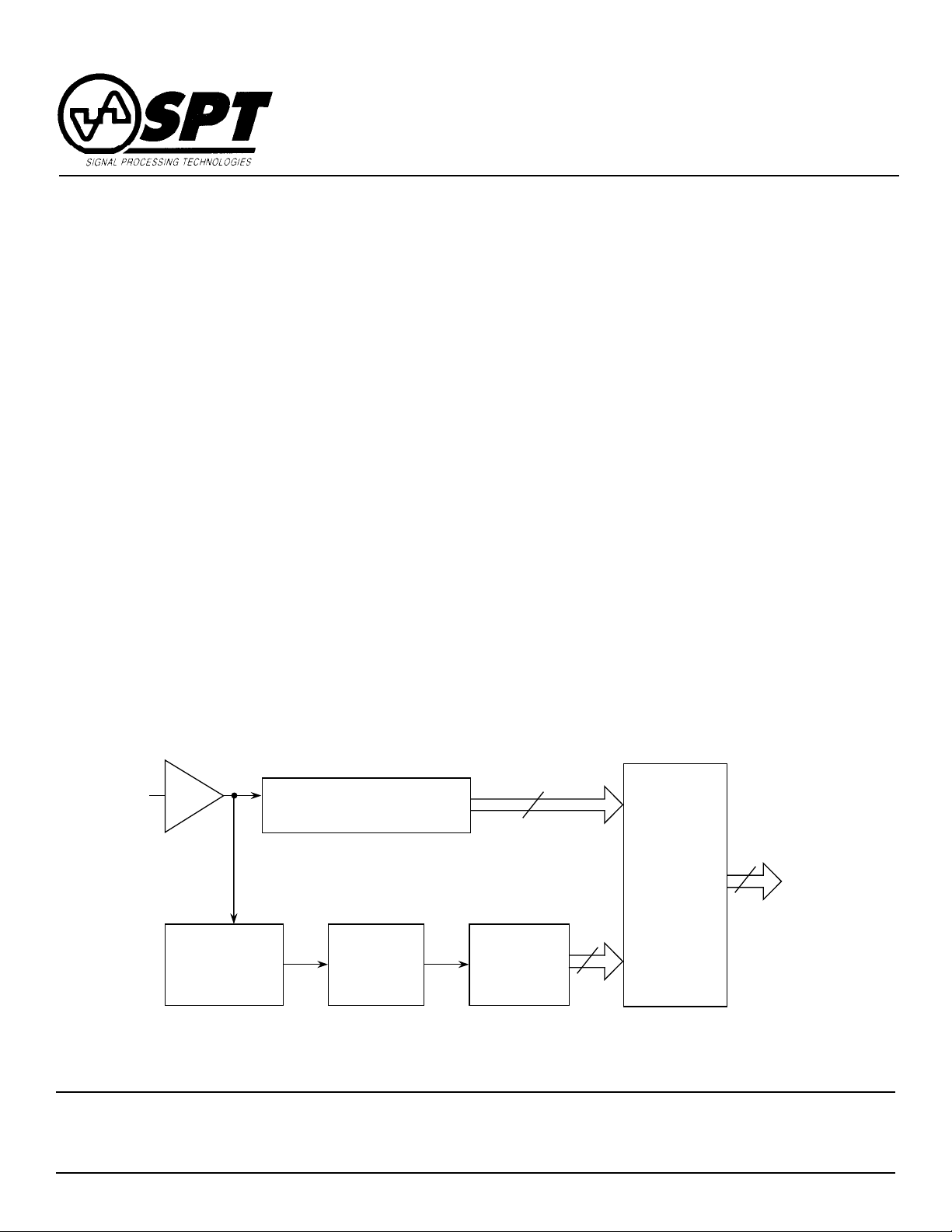
BLOCK DIAGRAM
V
Input
IN
Buffer
Analog Gain
Compression
Processor
Signal Processing Technologies, Inc.
4-Bit Flash
Converter
Track-and-Hold
Amplifiers
Asynchronous
SAR
4
Error
Correction,
Decoding
and
Output TTL
Drivers
8
4755 Forge Road, Colorado Springs, Colorado 80907, USA
Phone: (719) 528-2300 FAX: (719) 528-2370
12
Digital
Output
Page 2

ABSOLUTE MAXIMUM RATINGS (Beyond which damage may occur)1 25 °C
Supply Voltages
VCC...........................................................................+6 V
Output
Digital Outputs .............................................. 0 to -30 mA
VEE............................................................................ -6 V
Temperature
Input Voltages
Analog Input................................................ VFB≤VIN≤V
VFT, VFB. ....................................................+3.0 V, -3.0 V
Reference Ladder Current .....................................12 mA
CLK IN .......................................................................V
FT
CC
Operating Temperature ................................. 0 to +70 °C
Junction Temperature .........................................+175 °C
Lead Temperature, (soldering 10 seconds)........+300 °C
Storage Temperature................................ -65 to +150 °C
Note: 1. Operation at any Absolute Maximum Rating is not implied. See Electrical Specifications for proper nominal
applied conditions in typical applications.
ELECTRICAL SPECIFICATIONS
TA=T
unless otherwise specified.
PARAMETERS CONDITIONS LEVEL MIN TYP MAX UNITS
Resolution 12 Bits
DC Accuracy +25 °C
Analog Input f
Reference Input f
Timing Characteristics
Dynamic Performance
to T
MIN
Integral Nonlinearity ± Full Scale V ±2.0 LSB
Differential Nonlinearity 100 kHz Sample Rate V ±0.8 LSB
No Missing Codes VI Guaranteed
Input Voltage Range VI ±2.0 V
Input Bias Current TA=+25 °C I 30 60 µA
Input Resistance T
Input Capacitance V 5 pF
Input Bandwidth 3 dB Small Signal V 120 MHz
+FS Error V ±5.0 LSB
-FS Error V ±5.0 LSB
Reference Ladder Resistance VI 500 800 Ω
Reference Ladder Tempco V 0.8 Ω/°C
Maximum Conversion Rate VI 20 MHz
Overvoltage Recovery Time V 20 ns
Pipeline Delay (Latency) IV 1 Clock Cycle
Output Delay TA=+25 °C V 14 18 ns
Aperture Delay Time T
Aperture Jitter Time TA=+25 °C V 5 ps-RMS
Effective Number of Bits
=500 kHz 10.2 Bits
f
IN
f
=1.0 MHz 10.0 Bits
IN
=3.58 MHz 9.5 Bits
f
IN
, VCC=+5.0 V, VEE=-5.2 V, DVCC=+5.0 V, VIN=±2.0 V, VSB=-2.0 V, VST=+2.0 V, f
MAX
TEST TEST SPT7921
=1 MHz
CLK
=+25 °C, VIN=0 V I 100 300 kΩ
A
=1 MHz
CLK
=+25 °CV 1 ns
A
=20 MHz, 50% clock duty cycle,
CLK
Signal-To-Noise Ratio
(without Harmonics)
f
=500 kHz TA=+25 °C I 64 67 dB
IN
f
=1 MHz TA=+25 °C I 64 66 dB
IN
f
=3.58 MHz TA=+25 °C I 62 64 dB
IN
SPT
T
A=TMIN
T
A=TMIN
TA=T
MIN
to T
to T
to T
MAX
MAX
MAX
IV 58 61 dB
IV 58 60 dB
IV 58 60 dB
SPT7921
2 3/10/97
Page 3

ELECTRICAL SPECIFICATIONS
TA=T
MIN
to T
, VCC=+5.0 V, VEE=-5.2 V, DVCC=+5.0 V, VIN=±2.0 V, VSB=-2.0 V, VST=+2.0 V, f
MAX
=20 MHz, 50% clock duty cycle,
CLK
unless otherwise specified.
TEST TEST SPT7921
PARAMETERS CONDITIONS LEVEL MIN TYP MAX UNITS
Dynamic Performance
Harmonic Distortion
=500 kHz TA=+25 °C I 63 66 dB
f
IN
=1.0 MHz TA=+25 °C I 63 65 dB
f
IN
f
=3.58 MHz TA=+25 °C I 59 61 dB
IN
T
A=TMIN
T
A=TMIN
T
A=TMIN
to T
to T
to T
MAX
MAX
MAX
IV 59 62 dB
IV 59 61 dB
IV 57 59 dB
Signal-to-Noise and Distortion
=500 kHz TA=+25 °C I 60 63 dB
f
IN
f
=1.0 MHz TA=+25 °C I 60 62 dB
IN
f
=3.58 MHz TA=+25 °C I 57 59 dB
IN
Spurious Free Dynamic Range
Differential Phase
Differential Gain
2
2
Digital Inputs f
Logic 1 Voltage T
Logic 0 Voltage T
Maximum Input Current Low T
Maximum Input Current High T
T
T
T
1
TA=+25 °C V 74 dB
A=TMIN
A=TMIN
A=TMIN
to T
to T
to T
MAX
MAX
MAX
IV 55 58 dB
IV 55 57 dB
IV 54 56 dB
TA=+25 °C V 0.2 Degree
TA=+25 °C V 0.7 %
=1 MHz
CLK
=+25 °C I 2.4 4.5 V
A
=+25 °C I 0.8 V
A
=+25 °C I 0 +5 +20 µA
A
=+25 °C I 0 +5 +20 µA
A
Pulse Width Low (CLK) IV 20 ns
Pulse Width High (CLK) IV 20 300 ns
Digital Outputs f
Logic 1 Voltage T
=1 MHz
CLK
=+25 °C I 2.4 V
A
Logic 0 Voltage TA=+25 °C I 0.6 V
Power Supply Requirements
Voltages V
Currents I
DV
-V
CC
DI
-I
CC
EE
EE
CC
CC
TA=+25 °C I 135 150 mA
TA=+25 °C I 40 55 mA
TA=+25 °C I 45 70 mA
IV 4.75 5.0 5.25 V
IV 4.75 5.0 5.25 V
IV -4.95 -5.2 -5.45 V
Power Dissipation VI 1.1 1.3 W
Power Supply Rejection 5 V ±0.25 V, -5.2 ±0.25 V V 1.0 LSB
Typical thermal impedances (unsoldered, in free air):
32L sidebrazed DIP:
θ
= +50 °C/W
ja
44L cerquad:
θ
= +78 °C/W
ja
at 1 M/s airflow = +58 °C/W
θ
ja
θ
= +3.3 °C/W
jc
1
fIN = 1 MHz.
2
fIN = 3.58 and 4.35 MHz.
SPT
SPT7921
3 3/10/97
Page 4
TEST LEVEL CODES
TEST LEVEL
TEST PROCEDURE
All electrical characteristics are subject to the
following conditions:
All parameters having min/max specifications
are guaranteed. The Test Level column indicates the specific device testing actually performed during production and Quality Assurance inspection. Any blank section in the data
column indicates that the specification is not
tested at the specified condition.
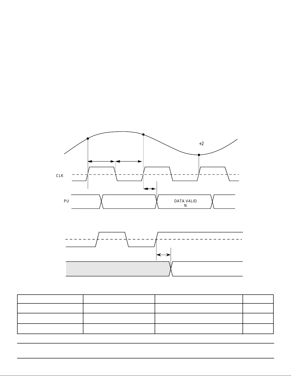
Figure 1A: Timing Diagram
N
tt
pwH pwL
II
III
IV
V
VI
I
100% production tested at the specified temperature.
100% production tested at TA = +25 °C, and sample
tested at the specified temperatures.
QA sample tested only at the specified temperatures.
Parameter is guaranteed (but not tested) by design
and characterization data.
Parameter is a typical value for information purposes
only.
100% production tested at TA = +25 °C. Parameter is
guaranteed over specified temperature range.
N+1
N+2
CLK
t
d
OUTPUT
DATA
N-2 N-1
DATA VALID
N
DATA VALID
N+1
Figure 1B: Single Event Clock
CLK
t
d
OUTPUT
DATA
DATA VALID
Table I - Timing Parameters
PARAMETERS DESCRIPTION MIN TYP MAX UNITS
t
d
t
pwH
CLK to Data Valid Prop Delay - 14 18 ns
CLK High Pulse Width 20 - 300 ns
t
pwL
SPT
CLK Low Pulse Width 20 - - ns
SPT7921
4 3/10/97
Page 5

SPECIFICATION DEFINITIONS
APERTURE DELAY
Aperture delay represents the point in time, relative to the
rising edge of the CLOCK input, that the analog input is
sampled.
APERTURE JITTER
The variations in aperture delay for successive samples.
DIFFERENTIAL GAIN (DG)
A signal consisting of a sine wave superimposed on various
DC levels is applied to the input. Differential gain is the
maximum variation in the sampled sine wave amplitudes at
these DC levels.
DIFFERENTIAL PHASE (DP)
A signal consisting of a sine wave superimposed on various
DC levels that is applied to the input. Differential phase is the
maximum variation in the sampled sine wave phases at these
DC levels.
EFFECTIVE NUMBER OF BITS (ENOB)
SINAD = 6.02N + 1.76, where N is equal to the effective
number of bits.
DIFFERENTIAL NONLINEARITY (DNL)
Error in the width of each code from its theoretical value.
(Theoretical = VFS/2N)
INTEGRAL NONLINEARITY (INL)
Linearity error refers to the deviation of each individual code
(normalized) from a straight line drawn from -Fs through +Fs.
The deviation is measured from the edge of each particular
code to the true straight line.
OUTPUT DELAY
Time between the clock's triggering edge and output data
valid.
OVERVOLTAGE RECOVERY TIME
The time required for the ADC to recover to full accuracy after
an analog input signal 125% of full scale is reduced to 50%
of the full-scale value.
SIGNAL-TO-NOISE RATIO (SNR)
The ratio of the fundamental sinusoid power to the total noise
power. Harmonics are excluded.
SINAD - 1.76
N =
+/- FULL-SCALE ERROR (GAIN ERROR)
Difference between measured full scale response
[(+Fs) - (-Fs)] and the theoretical response (+4 V -2 LSBs)
where the +FS (full scale) input voltage is defined as the
output transition between 1-10 and 1-11 and the -FS input
voltage is defined as the output transition between 0-00 and
0-01.
INPUT BANDWIDTH
Small signal (50 mV) bandwidth (3 dB) of analog input stage.
6.02
SIGNAL-TO-NOISE AND DISTORTION (SINAD)
The ratio of the fundamental sinusoid power to the total noise
and distortion power.
TOTAL HARMONIC DISTORTION (THD)
The ratio of the total power of the first 64 harmonics to the
power of the measured sinusoidal signal.
SPURIOUS FREE DYNAMIC RANGE (SFDR)
The ratio of the fundamental sinusoidal amplitude to the
single largest harmonic or spurious signal.
SPT
SPT7921
5 3/10/97
Page 6

PERFORMANCE CHARACTERISTICS
50
20
30
40
60
70
80
10
-1
10
0
10
1
THD vs Input Frequency
Input Frequency (MHz)
Total Harmonic Distortion (dB)
fs = 20 MSPS
Signal-to-Noise and Distortion (dB)
20
30
40
50
60
70
80
10
-1
10
0
10
1
SINAD vs Input Frequency
Input Frequency (MHz)
fs =20 MSPS
SNR, THD, SINAD vs Temperature
Temperature (°C)
SNR, THD, SINAD (dB)
55
60
65
70
75
50
f
s = 20 MSPS
f
IN
= 1 MHz
SINAD
THD
SNR
-25 0 +25 +50 +75
SNR vs Input Frequency
80
70
60
50
40
Signal-to-Noise Ratio (dB)
30
20
-1
10
SNR, THD, SINAD vs Sample Rate
80
70
60
50
= 1 MHz
f
IN
40
SNR, THD, SINAD (dB)
30
fs = 20 MSPS
0
Input Frequency (MHz)
10
SNR, THD
SINAD
1
10
20
0
10
0 dB
-30 dB
-60 dB
-120 dB
AMPLITUDE (dB)
-90 dB
012345
SPT
1
10
Sample Rate (MSPS)
SPT7921
Spectral Response
Frequency (MHz)
f
= 20 MSPS
S
= 1 MHz
f
IN
2
10
SPT7921
6 3/10/97
Page 7

TYPICAL INTERFACE CIRCUIT
The SPT7921 requires few external components to achieve
the stated operation and performance. Figure 2 shows the
typical interface requirements when using the SPT7921 in
normal circuit operation. The following section provides a
description of the pin functions and outlines critical performance criteria to consider for achieving the optimal device
performance.
POWER SUPPLIES AND GROUNDING
The SPT7921 requires -5.2 V and +5 V analog supply
voltages. The +5 V supply is common to analog VCC and
digital DVCC. A ferrite bead in series with each supply line is
intended to reduce the transient noise injected into the
analog VCC. These beads should be connected as closely as
possible to the device. The connection between the beads
and the SPT7921 should not be shared with any other
device. Each power supply pin should be bypassed as
closely as possible to the device. Use 0.1 µF for VEE and
VCC, and 0.01 µF for DVCC (chip caps are preferred).
AGND and DGND are the two grounds available on the
SPT7921. These two internal grounds are isolated on the
device. The use of ground planes is recommended to achieve
optimum device performance. DGND is needed for the
DVCC return path (40 mA typical) and for the return path for
all digital output logic interfaces. AGND and DGND should
be separated from each other and connected together only
at the device through a ferrite bead.
Figure 2 - Typical Interface Circuit
A Schottky or hot carrier diode connected between AGND
and VEE is required. The use of separate power supplies
between VCC and DVCC is not recommended due to potential power supply sequencing latch-up conditions. Using the
recommended interface circuit shown in figure 2 will provide
optimum device performance for the SPT7921.
VOLTAGE REFERENCE
The SPT7921 requires the use of two voltage references:
VFT and VFB. VFT is the force for the top of the voltage
reference ladder (+2.5 V typ), VFB (-2.5 V typ) is the force for
the bottom of the voltage reference ladder. Both voltages are
applied across an internal reference ladder resistance of 800
ohms. The +2.5 V voltage source for reference V
must be
FT
current limited to 20 mA maximum if a different driving circuit
is used in place of the recommended reference circuit shown
in figures 2 and 3. In addition, there are five reference ladder
taps (VST, VRT1, V
RT2, VRT3,
the top of the reference ladder (+2.0 V), V
and VSB). VST is the sense for
is the midpoint
RT2
of the ladder (0.0 V typ) and VSB is the sense for the bottom
of the reference ladder (-2.0 V). V
RT1
and V
are quarter
RT3
point ladder taps (+1.0 and -1.0 V typical, respectively). The
voltages seen at VST and VSB are the true full scale input
voltages of the device when VFT and VFB are driven to the
recommended voltages (+2.5 V and -2.5 V typical respectively). V
full scale input voltage of the device. V
and VSB should be used to monitor the actual
ST
RT1, VRT2
and V
RT3
should not be driven to the expected ideal values as is
commonly done with standard flash converters. When not
being used, a decoupling capacitor of .01 µF connected to
AGND from each tap is recommended to minimize high
frequency noise injection.
V
OUT
Tri m
32
-
IC2
OP-07
7
6
R1
100 Ω
± 2.5 V Max
6
5
- 5.2 V
4
C17
.01 µF
10 kΩ
30 kΩ
30 kΩ
C16
1 µF
+
1 µF
+
CLK
(TTL)
V
IN
(±2 V)
2
V
+ 5 V
C19
1 µF
+5 V
Notes to prevent latch-up due to power sequencing:
1) D1 = Schottky or hot carrier diode, P/N IN5817.
2) FB = Ferrite bead, Fair Rite P/N 2743001111
to be mounted as close to the device as possible. The ferrite bead to the ADC
connection should not be shared with any other device.
3) C1-C13 = Chip cap (recommended) mounted as close to the device's pin as
possible.
4) Use of a separate supply for VCC and DVCC is not recommended.
5) R1 provides current limiting to 45 mA.
6) C8, C9, C10 and C11 should be ten times larger than C12 and C13.
7) C10 = C11 = 0.1 µF cap in parallel with a 4.7 µF cap.
IC1
IN
+
(REF-03)
4
GND
1
+
10 kΩ
8
C18
.01 µF
C1
.01 µF
+2.5 V
C7
.01 µF
-2.5 V
.01 µF
.01 µF
.01 µF
.01 µF
.01 µF
CLK
17
V
IN
24
V
FT
21
C2
C3
C4
C5
C6
R
V
ST
22
2R
V
RT3
23
2R
V
RT2
25
2R
V
26
RT1
2R
V
27
SB
R
V
28
FB
EE
EE
V
V
18 31 19 30 20 29 16 32 1 15
C8
.1 µF
C9
.1 µF
D1
C15
10 µF
-5.2 V
(Analog)
+
AGND
COARSE
ANALOG
PRESCALER
SUCCESSIVE
INTERPOLATION
STA GE # 1
SUCCESSIVE
INTERPOLATION
STA GE # N
AGND
AGND
C10
C11
C14
10 µF
+
A/D
V
CC
FB
(Analog)
+5 V
14
D12
(OVERRANGE)
13
4
CC
CC
V
DV
.01 µF
.01 µF
FB
D11
D10
D E C O D I N G N E T W O R K
CC
DGND
DGND
DV
C12
C13
DGND
(MSB)
12
D9
11
10
D8
D7
9
8
D6
D5
7
6
D4
5
D3
4
D2
D1
3
2
D0
(LSB)
FB
D I G I T A L O U T P U T S
SPT
SPT7921
7 3/10/97
Page 8

Figure 3 - Analog Equivalent Input Circuit The drive requirements for the analog inputs are minimal
VCC
when compared to conventional Flash converters due to the
SPT7921’s extremely low input capacitance of only 5 pF and
very high input impedance of 300 kΩ. For example, for an
input signal of ± 2 V p-p with an input frequency of 10 MHz,
the peak output current required for the driving circuit is only
VIN
V
FT
628 µA.
CLOCK INPUT
The SPT7921 is driven from a single-ended TTL input (CLK).
ANALOG PRESCALER
For optimal noise performance, the clock input slew rate
should be a minimum of 6 ns. Because of this, the use of
fast
logic is recommended. The clock input duty cycle should be
50% where possible, but performance will not be degraded if
VEE
The analog input range will scale proportionally with respect
to the reference voltage if a different input range is required.
The maximum scaling factor for device operation is ± 20% of
kept within the range of 40-60%. However, in any case the
clock pulse width (tpwH) must be kept at 300 ns maximum to
ensure proper operation of the internal track and hold amplifier (see timing diagram). The analog input signal is latched on
the rising edge of the CLK.
the recommended reference voltages of VFT and VFB. However, because the device is laser trimmed to optimize performance with ± 2.5 V references, the accuracy of the device will
degrade if operated beyond a ± 2% range.
The clock input must be driven from fast TTL logic (VIH ≤4.5
V, T
<6 ns). In the event the clock is driven from a high
RISE
current source, use a 100 Ω resistor in series to current limit
to approximately 45 mA.
An example of a recommended reference driver circuit is
shown in figure 2. IC1 is REF-03, the +2.5 V reference with a
tolerance of 0.6% or +/- 0.015 V. The potentiometer R1 is 10
kΩ and supports a minimum adjustable range of up to
150 mV. IC2 is recommended to be an OP-07 or equivalent
device. R2 and R3 must be matched to within 0.1% with good
TC tracking to maintain a 0.3 LSB matching between VFT and
DIGITAL OUTPUTS
The format of the output data (D0-D11) is straight binary.
(See table II.) The outputs are latched on the rising edge of
CLK with a propagation delay of 14 ns (typ). There is a one
clock cycle latency between CLK and the valid output data.
(See timing diagram.)
VFB. If 0.1% matching is not met, then potentiometer R4 can
be used to adjust the VFB voltage to the desired level. R1 and
Table II - Output Data Information
R4 should be adjusted such that VST and VSB are exactly
+2.0 V and -2.0 V respectively.
The following errors are defined:
+FS error = top of ladder offset voltage = ∆(+FS -VST)
-FS error = bottom of ladder offset voltage = ∆(-FS -VSB)
Where the +FS (full scale) input voltage is defined as the
output 1 LSB above the transition of 1—10 and 1—11 and the
ANALOG INPUT OVERRANGE OUTPUT CODE
D12 D11-DO
>+2.0 V + 1/2 LSB 1 1111 1111 1111
+2.0 V -1 LSB O 1111 1111 111Ø
0.0 V O ØØØØ ØØØØ ØØØØ
-2.0 V +1 LSB O OOOO OOOO OOOØ
<-2.0 V O OOOO OOOO OOOO
-FS input voltage is defined as the output 1 LSB below the
transition of 0—00 and 0—01.
(Ø indicates the flickering bit between logic 0 and 1).
ANALOG INPUT
VIN is the analog input. The full scale input range will be 80%
of the reference voltage or ±2 volts with VFB=-2.5 V and
VFT=+2.5 V.
SPT
The rise times and fall times of the digital outputs are not
symmetrical. The propagation delay of the rise time is typically 14 ns and the fall time is typically 6 ns. (See figure 4.)
The nonsymmetrical rise and fall times create approximately
8 ns of invalid data.
SPT7921
8 3/10/97
Page 9

Figure 4 - Digital Output Characteristics
N
CLK IN
DATA OUT
(Actual)
DATA OUT
(Equivalent)
2.4 V
3.5 V
2.4 V
0.8 V
0.5 V
6 ns
typ.
(N-2)
(N-2)
Invalid
Data
tpd1
(14 ns typ.)
Invalid
Data
OVERRANGE OUTPUT
The overrange output (D12) is an indication that the analog
input signal has exceeded the full scale input voltage by
1 LSB. When this condition occurs, the outputs will switch to
logic 1s. All other data outputs are unaffected by this operation. This feature makes it possible to include the SPT7921
into higher resolution systems.
N+1
Rise Time
≤ 6 ns
Invalid
(N-1)
(N-1)
Data
Invalid
Data
(N)
(N-1)
EVALUATION BOARD
The EB7921 evaluation board is available to aid designers in
demonstrating the full performance of the SPT7921. This
board includes a reference circuit, clock driver circuit, output
data latches and an on-board reconstruction of the digital
data. An application note (AN7921) describing the operation
of this board as well as information on the testing of the
SPT7921 is also available. Contact the factory for price and
availability.
SPT
SPT7921
9 3/10/97
Page 10

PACKAGE OUTLINES
INCHES MILLIMETERS
SYMBOL MIN MAX MIN MAX
A 0.550 typ 13.97 typ
B 0.685 0.709 17.40 18.00
C 0.037 0.041 0.94 1.04
D 0.016 typ 0.41 typ
E 0.008 typ 0.20 typ
F 0.027 0.051 0.69 1.30
G 0.006 typ 0.15 typ
H 0.080 0.150 2.03 3.81
32-Lead Sidebrazed
32
1
G
A
E
F
C
B
D
H
I
J
INCHES MILLIMETERS
SYMBOL MIN MAX MIN MAX
A 0.081 0.099 2.06 2.51
B 0.016 0.020 0.41 0.51
C 0.095 0.105 2.41 2.67
D .050 typ 1.27
E 0.040 1.02
F 0.175 0.225 4.45 5.72
G 1.580 1.620 40.13 41.15
H 0.585 0.605 14.86 15.37
I 0.009 0.012 0.23 0.30
J 0.600 0.620 15.24 15.75
44-Lead Cerquad
C
D
A
B
SPT
A B
0 - 5°
E
F
H
G
SPT7921
10 3/10/97
Page 11

PIN ASSIGNMENTS PIN FUNCTIONS
DGND
D10
D11
D12
DGND
DV
D0
D1
D2
D3
D4
D5
D6
D7
D8
D9
CC
1
2
3
4
5
6
7
8
9
10
11
12
13
14
15
16
DØ
D1
44
43
32L Sidebrazed
CC
AGND
DV
V
N/C
N/C
EE
36
39
38
37
40
N/C
42
DGND
41
CC
DV
32
CC
V
31
EE
AGND
30
29
V
CC
28
V
FB
V
27
SB
26
V
RT1
25
V
RT2
24
V
IN
V
23
RT3
22
V
ST
21
V
FT
20
V
CC
19
AGND
18
V
EE
17
CLK
V
N/C
35
34
Name Function
DGND Digital Ground
AGND Analog Ground
D0-D11 TTL Outputs (D0=LSB)
D12 TTL Output Overrange
CLK Clock Input
V
EE
V
CC
V
RT1-VRT3
V
IN
DV
CC
V
FT
V
ST
V
FB
V
SB
-5.2 V Supply
+5.0 V supply
Voltage Reference Taps
Analog Input
Digital +5.0 V Supply (TTL Outputs)
Force for Top of Reference Ladder
Sense for Top of Reference Ladder
Force for Bottom of Reference Ladder
Sense for Bottom of Reference Ladder
D10
D11
N/C
1
D2
2
D3
D4
3
D5
4
5
D6
D7
6
D8
7
8
D9
9
10
11
44L Cerquad
14
12
13
DGND
N/C
D12
CC
20
17
15
16
CLK
DV
N/C
18
N/C
21
19
V
N/C
EE
22
AGND
N/C
33
N/C
V
32
FB
V
31
SB
V
30
RT1
V
29
RT2
V
28
IN
V
27
RT3
V
26
ST
V
25
FT
N/C
24
V
23
CC
ORDERING INFORMATION
PART NUMBER TEMPERATURE RANGE PACKAGE
SPT7921SCJ 0 to +70 °C 32L Sidebrazed Dip
SPT7921SCQ 0 to +70 °C 44L Cerquad
Signal Processing Technologies, Inc. reserves the right to change products and specifications without notice. Permission is hereby expressly
granted to copy this literature for informational purposes only. Copying this material for any other use is strictly prohibited.
WARNING - LIFE SUPPORT APPLICATIONS POLICY - SPT products should not be used within Life Support Systems without the specific
written consent of SPT. A Life Support System is a product or system intended to support or sustain life which, if it fails, can be reasonably
expected to result in significant personal injury or death.
Signal Processing Technologies believes that ultrasonic cleaning of its products may damage the wire bonding, leading to device
failure. It is therefore not recommended, and exposure of a device to such a process will void the product warranty.
SPT7921
SPT
11 3/10/97
 Loading...