

Page 1
A
A
A
A
A
A
A
A
A
A
A
A
A
A
A
A
A
A
A
A
A
A
A
A
A
A
A
A
FEATURES
• 10-Bit, 100 MSPS Analog-to-Digital Converter
• Monolithic Bipolar
• Single-Ended Bipolar Analog Input
• -1.0 V to +1.0 V Analog Input Range
• Internal Sample-and-Hold
• Internal Voltage Reference
• Programmable Data Output Formats
• Single Ended TTL Outputs
• Differential ECL Clock Input
• ECL Version Available as the SPT7870
SPT7871
10-BIT, 100 MSPS TTL A/D CONVERTER
APPLICATIONS
• Professional Video
• HDTV
• Communications
• Imaging
• Digital Oscilloscopes
GENERAL DESCRIPTION
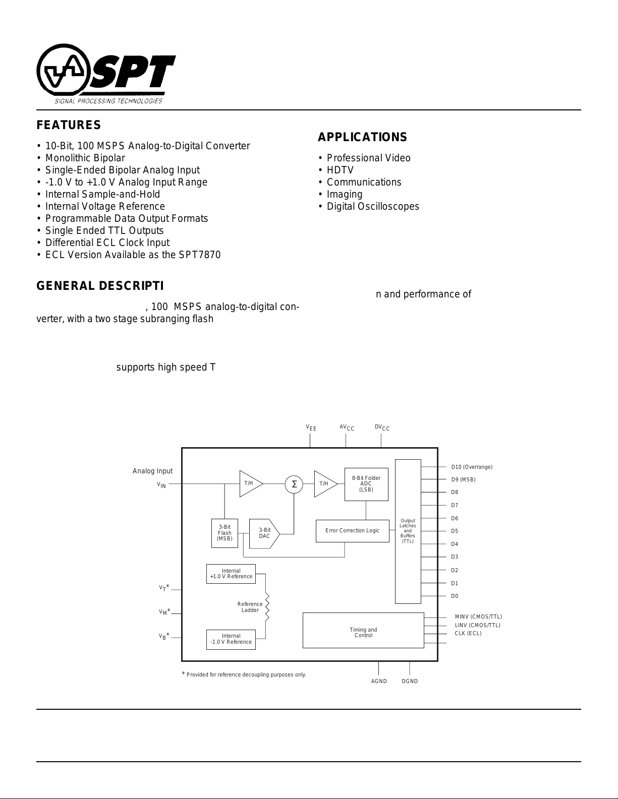
The SPT7871 is a 10-bit, 100 MSPS analog-to-digital converter, with a two stage subranging flash/folder architecture.
The bipolar, single-ended analog input provides an easy
interface for most applications. Programmable data output
formats provide additional ease of implementation and flexibility. The device supports high speed TTL outputs.
BLOCK DIAGRAM
AAAAAAAAAAAAAAAAAAAAAAAAAAAAA
Analog Input
Signal Processing Technologies, Inc.
Phone: (719) 528-2300 FAX: (719) 528-2370 Website: http://www.spt.com E-Mail: sales@spt.com
AAAAAAAAAAAAAAAAAAAAAAAAAAAAA
AAAAAAAAAAAAAAAAAAAAAAAAAAAAA
V
AAAAAAAAAAAAAAAAAAAAAAAAAAAAA
IN
T/H
Σ
AAAAAAAAAAAAAAAAAAAAAAAAAAAAA
AAAAAAAAAAAAAAAAAAAAAAAAAAAAA
AAAAAAAAAAAAAAAAAAAAAAAAAAAAA
AAAAAAAAAAAAAAAAAAAAAAAAAAAAA
AAAAAAAAAAAAAAAAAAAAAAAAAAAAA
AAAAAAAAAAAAAAAAAAAAAAAAAAAAA
3-Bit
Flash
(MSB)
3-Bit
DAC
AAAAAAAAAAAAAAAAAAAAAAAAAAAAA
AAAAAAAAAAAAAAAAAAAAAAAAAAAAA
AAAAAAAAAAAAAAAAAAAAAAAAAAAAA
AAAAAAAAAAAAAAAAAAAAAAAAAAAAA
AAAAAAAAAAAAAAAAAAAAAAAAAAAAA
V
*
T
AAAAAAAAAAAAAAAAAAAAAAAAAAAAA
AAAAAAAAAAAAAAAAAAAAAAAAAAAAA
AAAAAAAAAAAAAAAAAAAAAAAAAAAAA
V
*
M
AAAAAAAAAAAAAAAAAAAAAAAAAAAAA
AAAAAAAAAAAAAAAAAAAAAAAAAAAAA
AAAAAAAAAAAAAAAAAAAAAAAAAAAAA
V
*
B
AAAAAAAAAAAAAAAAAAAAAAAAAAAAA
AAAAAAAAAAAAAAAAAAAAAAAAAAAAA
*
Provided for reference decoupling purposes only.
Internal
AAAAA
+1.0 V Reference
Reference
Ladder
Internal
-1.0 V Reference
AAAAA
4755 Forge Road, Colorado Springs, Colorado 80907, USA
The resolution and performance of this device makes it well
suited for professional video and HDTV applications. The onchip track-and-hold provides for excellent AC performance
enabling this device to be a converter of choice for RF
communications and digital sampling oscilloscopes. The
SPT7871 is available in a 44L cerquad package in the
industrial temperature range and in die form.
EE
T/H
Error Correction Logic
AV
CC
Timing and
8-Bit Folder
ADC
(LSB)
Control
AGND
DV
CC
D10 (Overrange)
D9 (MSB)
D8
D7
Output
Latches
and
Buffers
(TTL)
DGND
D6
D5
D4
D3
D2
D1
D0
MINV (CMOS/TTL)
LINV (CMOS/TTL)
CLK (ECL)
NCLK (ECL)
V
AAAAAAAAAAAAA
AAAAAAAAAAAAA
AAAAAAAAAAAAA
Page 2

ABSOLUTE MAXIMUM RATING (Beyond which damage may occur)
Supply Voltages
AV
........................................................................
CC
DV
........................................................................
CC
V
.............................................................................
EE
0 to +6.5 V
0 to +6.5 V
0 to -6.5 V
Output
Digital Outputs ......................................... +30 to -30 mA
Temperature
1
Operating Temperature .............................-40 to + 85 °C
Input Voltages
Analog Input............................................. VEE≤VIN≤V
LINV/MINV Inputs .......................... -0.5 V to VCC +0.5 V
CC
Junction Temperature ........................................ + 175 °C
Lead, Soldering (10 seconds)............................ + 300 °C
Storage ....................................................-60 to + 150 °C
CLK/NCLK Inputs........................................... VEE to 0 V
Note: 1. Operation at any Absolute Maximum Ratings is not implied. See Electrical Specifications for proper nominal applied
conditions in typical applications.
ELECTRICAL SPECIFICATIONS
TA = +25 °C , DV
PARAMETERS CONDITIONS LEVEL MIN TYP MAX UNITS
DC Performance
Resolution 10 Bits
Differential Linearity f
Integral Linearity, Best Fit f
No Missing Codes f
Analog Input
Input Voltage Range V ±1.0 V
Input Bias Current I -100 25 100 µA
Input Resistance I 50 150 kΩ
Input Capacitance V 5 pF
Input Bandwidth Full Power IV 150 180 MHz
±FS Offset Error I ±20 ±100 mV
Timing Characteristics
Minimum Conversion Rate V 2 MSPS
Maximum Conversion Rate IV 100 MSPS
Pipeline Delay (Latency) IV 2 Clock
Transient Response V 10 ns
Overvoltage Recovery Time V 10 ns
Output Delay (td)V3ns
Aperture Delay Time V 1 ns
Aperture Jitter Time V 5 ps (rms)
Dynamic Performance
Effective Number of Bits
fIN = 10 MHz I 8.1 8.5 Bits
fIN = 25 MHz I 8.1 8.5 Bits
fIN = 25 MHz f
fIN = 50 MHz I 7.5 7.8 Bits
fIN = 50 MHz f
Signal-To-Noise Ratio
fIN = 10 MHz I 52 54 dB
fIN = 25 MHz I 52 54 dB
fIN = 25 MHz f
fIN = 50 MHz I 52 54 dB
fIN = 50 MHz f
Total Harmonic Distortion
fIN = 10 MHz I -56 -62 dBc
fIN = 25 MHz I -56 -60 dBc
fIN = 25 MHz f
fIN = 50 MHz I -48 -51 dBc
fIN = 50 MHz f
CC
=AV
= +5.0 V, V
CC
1
= -5.2 V, V
EE
= ±1.0 V, f
IN
TEST TEST
= 6.4 MHz I -1.0 ±0.5 ±1.25 LSB
Clock
= 6.4 MHz I ±1.0 ±2.0 LSB
Clock
Full Temperature V ±2.5 LSB
= 6.4 MHz I Guaranteed
Clock
Full Temperature V 100 kΩ
= 100 MHz V 8.0 Bits
clock
= 100 MHz V 7.5 Bits
clock
= 100 MHz V 51 dB
clock
= 100 MHz V 50 dB
clock
= 100 MHz V -56 dBc
clock
= 100 MHz V -50 dBc
clock
= 80 MHz, 50% clock duty cycle, unless otherwise specified.
clock
SPT
SPT7871
2 9/7/98
Page 3

ELECTRICAL SPECIFICATIONS
TA = +25 °C , DV
PARAMETERS CONDITIONS LEVEL MIN TYP MAX UNITS
Dynamic Performance
Signal-to-Noise + Distortion (SINAD)
fIN =10 MHz I 51 53 dB
fIN = 25 MHz I 51 53 dB
fIN = 25 MHz f
fIN = 50 MHz I 47 49 dB
fIN = 50 MHz f
Spurious Free Dynamic Range
fIN = 10 MHz V 65 dB FS
fIN = 25 MHz V 63 dB FS
fIN = 50 MHz V 52 dB FS
Two-Tone IMD Rejection
Differential Phase V 0.5 Degree
Differential Gain V 1 %
Power Supply Requirements
AVCC Supply Voltage IV 4.75 5.0 5.25 V
DVCC Supply Voltage IV 4.75 5.0 5.25 V
VEE Supply Voltage IV -4.95 -5.2 -5.45 V
VCC Supply Current Full Temperature VI 210 248 mA
VEE Supply Current Full Temperature VI 128 151 mA
Power Dissipation Full Temperature VI 1.7 2.0 W
Power Supply Rejection Ratio IV 30 dB
Digital Inputs
LINV, MINV V CMOS/TTL Logic
Clock Inputs
Logic 1 Voltage (ECL) VI -1.1 V
Logic 0 Voltage (ECL) VI -1.5 V
Maximum Input Current Low VI -100 +100 µA
Maximum Input Current High VI -100 +100 µA
Pulse Width Low (CLK) IV 4.0 250 ns
Pulse Width High (CLK) IV 4.0 250 ns
Rise/Fall Time 20% to 80% IV 1.5 ns
Digital Outputs
Logic 1 Voltage (TTL) 2 mA VI 2.4 2.8 V
Logic 0 Voltage (TTL) 2 mA VI 0.5 0.8 V
t
Rise
t
Fall
1
2048 pt FFT using distortion harmonics 2 through 10.
2
Measured as a second order (f1-f2) intermodulation product from a two-tone test with each input tone at 0 dBm.
CC
=AV
= +5.0 V, V
CC
2
= -5.2 V, V
EE
= ±1.0 V, f
IN
TEST TEST
= 100 MHz V 50 dB
clock
= 100 MHz V 47 dB
clock
10% to 90% V 2.0 ns
10% to 90% V 2.0 ns
= 80 MHz, 50% clock duty cycle, unless otherwise specified.
clock
V -65 dBc
TEST LEVEL CODES
All electrical characteristics are subject to the
following conditions:
All parameters having min/max specifications
are guaranteed. The Test Level column indicates the specific device testing actually performed during production and Quality Assurance inspection. Any blank section in the data
column indicates that the specification is not
tested at the specified condition.
Unless otherwise noted, all tests are pulsed
tests; therefore, TJ = TC = TA.
SPT
TEST LEVEL
I
II
III
IV
V
VI
3 9/7/98
TEST PROCEDURE
100% production tested at the specified temperature.
100% production tested at TA = +25 °C, and sample
tested at the specified temperatures.
QA sample tested only at the specified temperatures.
Parameter is guaranteed (but not tested) by design
and characterization data.
Parameter is a typical value for information purposes
only.
100% production tested at TA = +25 °C. Parameter is
guaranteed over specified temperature range.
SPT7871
Page 4

Figure 1 - Timing Diagram
N
N+1
t
clk
t
pwh
CLK
OUTPUT
DATA
Table I - Data Output Timing Parameters
Timing Parameter Minimum Typical Maximum
f
clock
Clock Pulse Width High (t
Clock Pulse Width Low (t
Switching Delay (td) 3 ns
Clock Latency 2 clock cycles
N-3 N-2
pwh
pwl
t
pwl
d
t
DAT A V ALID
2 MHz 100 MHz
) 4.0 ns 250 ns
) 4.0 ns 250 ns
N+2
DAT A V ALID
N-1
N
THEORY OF OPERATION
The SPT7871 uses a two stage subranging architecture
incorporating a 3-bit flash MSB conversion stage followed by
an 8-bit interpolating folder conversion stage. Digital error
correction logic combines the results of both stages to produce a 10-bit data conversion digital output.
The analog signal is input directly to the 3-bit flash converter
which performs a 3-bit conversion and in turn drives an
internal DAC used to set the second stage voltage reference
level. The 3-bit result from the flash conversion is input to the
digital error correction logic and used in calculation of the
upper most significant bits of the data output.
The analog input is also input directly to an internal track-andhold amplifier. The signal is held and amplified for use in the
second stage conversion. The output of the track-and-hold is
input into a summing junction that takes the difference
between the track-and-hold amplifier and the 3-bit DAC
output. The residual is captured by a second track-and-hold
which holds and amplifies this residual voltage.
The residual held by the track-and-hold amplifier is input to an
8-bit interpolating folder stage for data conversion. The 8-bit
converted data from the folder stage is input into the digital
error correction logic and used in calculation of the lower
significant bits.
The error correction logic incorporates a proprietary scheme
for compensation of any internal offset and gain errors that
might exist to determine the 10-bit conversion result. The
resultant 10-bit data conversion is internally latched and
presented on the data output pins via buffered output drivers.
TYPICAL INTERFACE CIRCUIT
The SPT7871 requires few external components to achieve
the stated operation and performance. Figure 2 shows the
typical interface requirements when using the SPT7871 in
normal circuit operation. The following section is a description
of the pin functions and outlines critical performance criteria
to consider for achieving the optimal device performance.
POWER SUPPLIES AND GROUNDING
The SPT7871 requires the use of three supply voltages: V
AVCC and DVCC. The VEE and AVCC supplies should be
treated as analog supply sources. This means the VEE and
VCC ground returns of the device should both be connected
to the analog ground plane. Each power supply pin should be
bypassed as closely as possible to the device with .01 µF and
2.2 µF capacitors as shown in figure 2.
The two grounds available on the SPT7871 are AGND and
DGND. DGND is used only for TTL outputs and is to be
referenced to the output pullup voltage. These grounds are
not tied together internal to the device. The use of ground
planes is recommended to achieve the best performance of
the SPT7871. The AGND and the DGND ground planes
should be separated from each other and only connected
together at the device through an inductance or ferrite bead.
Doing this will minimize the ground noise pickup.
EE,
SPT
SPT7871
4 9/7/98
Page 5

ANALOG INPUT
The SPT7871 has a single-ended analog input with a bipolar
input range from -1 V to +1 V. The bipolar input allows for
easier interface by external op amps when compared to
unipolar input devices. Because the input common mode is
0 V, the external op amp can operate without a voltage offset
on the output, thereby maximizing op amp head room and
minimizing distortion.
In addition, the 0 V common mode allows for a very simple DC
coupled analog input connection if desired. The current drive
requirements for the analog input are minimal when compared to conventional flash converters due to the SPT7871’s
low input capacitance of only 5 pF and very high input
impedance of 150 kΩ.
CLOCK INPUTS
The clock inputs are designed to be driven differentially
with ECL levels. For optimal noise performance, the clock
input rise time should be a maximum of 1.5 ns. Because of
this, the use of
signal is latched on the rising edge of the CLK.
The clock may be driven single-ended since the NCLK pin is
internally biased to -1.3 V. NCLK may be left open but a
.01 µF bypass capacitor from NCLK to AGND is recommended. NOTE: System performance may be degraded due
to increased clock noise or jitter.
The performance of the SPT7871 is specified and tested with
a 50% clock duty cycle. However, at sample rates greater
than 80 MSPS, additional gains in the dynamic performance
of the device may be obtained by adjusting the clock duty
cycle. Typically, operation near 55% duty cycle will yield
improved results.
INTERNAL VOLTAGE REFERENCE
The SPT7871 incorporates an on-chip voltage reference.
The top and bottom reference voltages are each internally
tied to their respective top and bottom of the internal reference ladder. The pins for the voltage references and the
ladder (including the center of the ladder) are brought out to
pins on the device for decoupling purposes only (pins VT, V
and VB). A .01 µF capacitor should be used on each pin and
tied to AGND. See the typical interface circuit (figure 2).
The internal voltage reference and the internal error correction logic eliminate the need for driving externally the voltage
reference ladder. In fact,
not be driven
internal error correction circuitry already compensates for the
internal voltage and no improvement will result.
fast
logic is recommended. The analog input
M,
the voltage reference ladder should
with an external voltage reference source as the
DIGITAL OUTPUTS
DIGITAL OUTPUT DATA FORMAT - D0 - D9
D0 is the least-significant bit for the digital data output, and D9
is the most-significant bit. Four data output formats are
available and are controlled by the MINV and LINV pins.
Table III shows the four possible output formats possible as
a function of MINV and LINV. Table II shows the output coding
data format versus analog input voltage relationship.
Table II - Output Coding Data Format
V
IN
>+1.0 V 1 11 1111 1111 01 1111 1111
(+FS) 0 11 1111 1111 01 1111 1111
+1.0 V -1 LSB 0 11 1111 1110 01 1111 1110
0.0 V 0 10 0000 0000 00 0000 0000
-1.0 V +1 LSB 0 00 0000 0001 10 0000 0001
(-FS) 0 00 0000 0000 10 0000 0000
<-1.0 V 0 00 0000 0000 10 0000 0000
*Refer to table III for possible output formats.
OVERRANGE BIT - D10
D10 is the overrange bit which is asserted whenever the
analog input signal exceeds the positive full scale input by
1 LSB. When this condition occurs the D10 bit will be asserted
to logic high and remain high continuously until the overrange
condition is removed from the input.
All other output signals will also stay at their maximum
encoded output throughout this condition. D10 is not asserted for an underscale condition when the input exceeds
the negative full scale.
DIGITAL OUTPUT DATA TIMING
The data is presented on the output pins two clock cycles after
the input is sampled with an additional output delay of
typically 3 ns. The data is held valid for one clock cycle. Refer
to the timing diagram shown in figure 1.
DIGITAL OUTPUT CONTROL PINS - MINV, LINV
Two digital output control pins control the digital output
format. See table III. The MINV pin is a CMOS/TTL-compatible input. It inverts the most-significant bit (D9) when tied to
+5 V. The most-significant bit (D9) is noninverted when MINV
is tied to ground or floated. The MINV pin is internally pulled
down to ground.
The LINV pin is a CMOS/TTL-compatible input. It inverts the
least-significant bits (D8 through D0) when tied to +5 V. The
least-significant bits (D8 through D0) are noninverted when
LINV is tied to ground or floated. The LINV pin is internally
pulled down to ground.
Table III - Data Output Bits
MINV LINV Description of Data
0 V 0 V Binary (Noninverted)
0 V +5 V Two's Complement (Inverted)
+5 V 0 V Two's Complement (Noninverted)
+5 V +5 V Binary (Inverted)
D10 D9…D0 (Binary*) D9…D0 (2's Comp*)
0 01 1111 1111 11 1111 1111
SPT
SPT7871
5 9/7/98
Page 6

TYPICAL PERFORMANCE CHARACTERISTICS
0
Dynamic Performance vs. Sample Rate
65
60
55
dB
50
45
40
60 70 80 90 100 110
Dynamic Performance vs. Input Frequency
60
THD
55
50
dB
45
Input Frequency = 25MHz
THD
SNR
SINAD
Sample Rate (MSPS)
Sample Rate = 100 MSPS
SINAD
SNR
Dynamic Performance vs. Input Frequency
70
65
60
55
dB
50
45
40
0 20406080100
Dynamic Performance vs. Temperature
65
60
dB
55
Sample Rate = 80 MSPS
THD
SNR
SINAD
Input Frequency (MHz)
Sample Rate = 80 MSPS
Input Frequency = 25 MHz
THD
SNR
40
35
020406080100
Input Frequency (MHz)
Single Tone at 4.9 MHz
0
-10
-20
-30
-40
-50
-60
-70
-80
-90
Power Relative to ADC Full Scale (dB)
010203040
Sample Rate = 80 MSPS
Frequency (MHz)
SINAD
50
-25 0 25 50 75 10
Temperature (°C)
Single Tone at 14.9 MHz
0
-10
-20
-30
-40
-50
-60
-70
-80
-90
Power Relative to ADC Full Scale (dB)
0
Sample Rate = 80 MSPS
10 20 30 40
Frequency (MHz)
SPT
SPT7871
6 9/7/98
Page 7

TTL DIGITAL OUTPUT LEVELS
AGND
CLK
26 kΩ
AV
CC
V
EE
6 kΩ
52 kΩ
-1.3 V
(ESD)
(ESD)
NCLK
26 kΩ
(ESD)
(ESD)
DGND
(ESD)
(ESD)
TTL OUT
DV
CC
INCHES MILLIMETERS
SYMBOL MIN MAX MIN MAX
A 0.550 typ 13.97 typ
B 0.685 0.709 17.40 18.00
C 0.037 0.041 0.94 1.04
D 0.016 typ 0.41 typ
E 0.008 typ 0.20 typ
F 0.027 0.051 0.69 1.30
G 0.006 typ 0.15 typ
H 0.080 0.150 2.03 3.81
The SPT7871 supports TTL and some CMOS logic levels.
(Refer to minimum high voltage level for selected digital parts
that will interface with the SPT7871.) It has single-ended outputs
that are driven off a separate +5 V digital supply (DVCC).
THERMAL MANAGEMENT
SPT recommends that a heat sink be used for this device to
ensure rated performance. A heat sink in still air provides
Figure 2 - Typical Interface Circuit
+A5-A5.2
FB2
FB3
**
AGND
V
EE
Analog
Input
ECL
Differential
Clock Input
V
.01
.01
.01
IN
V
T
V
M
SPT7871
V
B
X
CLK
X
CLK
MINV
Notes:
1) = Line termination
X
2) = 0.01 µF chip cap. in parallel with
*
2.2 µF, tant cap.
3) Immediate output buffer is highly recommended
to optimize the performance due to reflection.
AV
CC
LINV
.01
DGND
DV
CC
D10
D9
D8
D7
D6
D5
D4
D3
D2
D1
D0
FB1
+A5
+A5 -A5.2
10 µF
10µF
+
+
+5 V -5.2 VA GND
Interfacing
Logics
+D5
+D5
10 µF
+
+5V DGND
adequate thermal performance under laboratory tests. Air
flow may be required for operation at elevated ambient
temperature. SPT recommends that the junction temperature be maintained under +150 °C.
The thermal impedance values for the cerquad package are
θJC = 3.3 °C/W and θ
70 °C/W (junction to ambient in still
JA =
air with no heat sink).
Figure 3 - Clock Input Equivalent Circuit
Figure 4 - Digital Outputs Equivalent Circuit
44
C
1
D
SPT
A
B
A B
PACKAGE OUTLINE
44L Cerquad
0 - 5°
E
7 9/7/98
H
G
F
SPT7871
Page 8

PIN ASSIGNMENTS
PIN FUNCTIONS
DØ
D1
D2
D3
D4
D5
D6
D7
D8
D9
D1Ø
Name I/O Function
V
IN
D0-D
D
10
I Analog Input
O Digital Output Data (D0 = LSB) (TTL)
9
O Overflow (TTL)
N/C
44
DGND
DV
43
42
CC
LINV
41
N/C
40
CC
AGND
37
36
CC
AGND
AV
35
AV
34
EE
EE
V
V
38
39
CLK I Clock (Internal Pull-Down to Ground)
1
2
3
4
5
6
7
8
9
10
11
12
13
N/C
DGND
44L Cerquad
16
15
14
CC
DV
MINV
CLK
17
NCLK
18
N/C
19
EE
V
20
V
EE
22
21
AGND
AGND
V
33
B
N/C
32
31
N/C
V
30
M
29
N/C
V
28
IN
N/C
27
26
N/C
V
25
T
AV
24
CC
AV
23
CC
NCLK I Inverted Clock (ECL)
(Internal Pull-Down to -1.3 V)
LINV I Invert Least Significant Bits (D0-D8);
CMOS/TTL Level; Invert=+5 V;
Internal Pull-Down to Ground
MINV I Invert MSB (D9);
CMOS/TTL Level; Invert=+5 V;
Internal Pull-Down to Ground
V
T
N/A Internal Top Reference Decoupling
(+1 V typical)
V
M
N/A Internal Mid-Point Reference Decoupling
(0 V typical)
V
B
N/A Internal Bottom Reference Decoupling
(-1 V typical)
AV
DV
V
CC
CC
EE
I +5 V Analog Supply
I +5 V Digital Supply
I -5.2 V Supply
N/C - Not Connected
AGND I Analog Ground
DGND I Digital Ground
ORDERING INFORMATION
PART NUMBER TEMPERATURE RANGE PACKAGE
SPT7871SIQ -40 to +85 °C 44L Cerquad
SPT7871SCU +25 °C Die*
*Please see the die specification for guaranteed electrical performance.
Signal Processing Technologies, Inc. reserves the right to change products and specifications without notice. Permission is hereby expressly
granted to copy this literature for informational purposes only. Copying this material for any other use is strictly prohibited.
WARNING - LIFE SUPPORT APPLICATIONS POLICY - SPT products should not be used within Life Support Systems without the specific
written consent of SPT. A Life Support System is a product or system intended to support or sustain life which, if it fails, can be reasonably
expected to result in significant personal injury or death.
Signal Processing Technologies believes that ultrasonic cleaning of its products may damage the wire bonding, leading to device
failure. It is therefore not recommended, and exposure of a device to such a process will void the product warranty.
SPT7871
SPT
8 9/7/98
 Loading...