

Page 1
SPT7868
10-BIT, 80 MSPS A/D CONVERTER
PRELIMINARY INFORMATION
FEATURES
• 80 MSPS maximum sample r ate
• 9.2 eff ectiv e n umber of bits at ƒIN = 15 MHz and
ƒS = 80 MSPS
•2 V
• Diff erential input 2.5 V common mode
• Internal or external voltage ref erence
• Common-mode v oltage reference output
• +3.3 V / +5 V digital output logic compatibility
• +5 V analog power supply
full-scale input range
P-P
GENERAL DESCRIPTION
The SPT7868 is a 10-bit, 80 MSPS analog-to-digital converter with low power dissipation at only 627 mW typical at
80 MSPS with a power supply of +5.0 V. The digital outputs
are +3 V or +5 V, and are user selectable. The SPT7868
has incorporated proprietary circuit design and CMOS
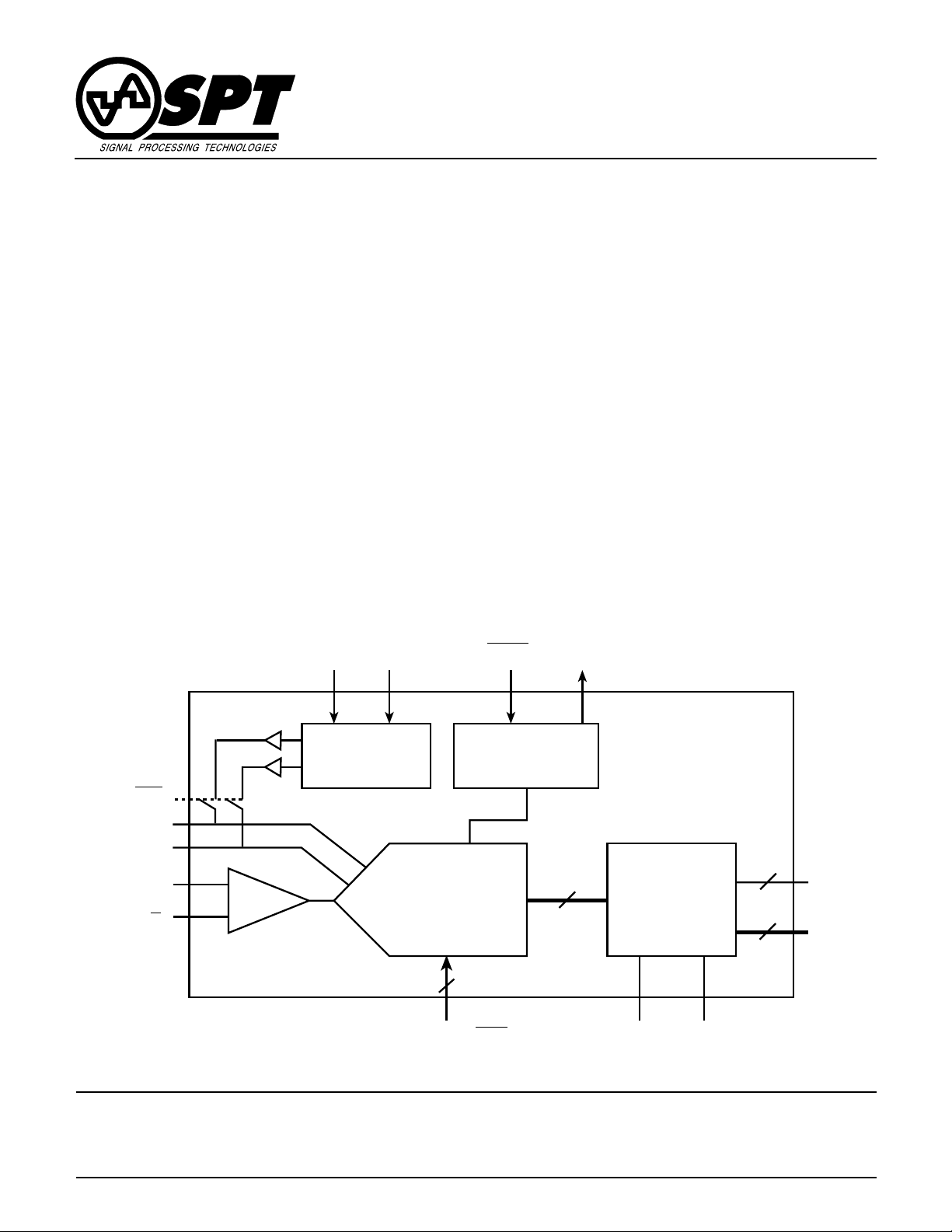
BLOCK DIAGRAM
V
DD
GND
APPLICATIONS
• High-speed applications where low power dissipation is
required
• Video imaging
• Medical imaging
• Radar receivers
• IR imaging
• Digital communications
processing technologies to achieve its advanced performance. Inputs and outputs are TTL/CMOS compatible to
interface with TTL/CMOS logic systems. Output data format is straight binary.
The SPT7868 is available in a 28-lead SSOP package
over the industrial temperature range.
Sleep
V
CM
Bias
Cell
10
Data
Output
Latches
& Buffers
1
10
EXT/INT
REF
REF
V
IN
V
IN
Bandgap
Reference
H
L
10-BIT
THA
80 MSPS
ADC
2
CLK, CLK
GND OV
DD
Signal Processing Technologies, Inc.
4755 Forge Road, Colorado Springs, Colorado 80907, USA
Phone: 719-528-2300 Fax: 719-528-2370 Web Site: http://www .spt.com e-mail: sales@spt.com
OR
D0D9
Page 2
ABSOLUTE MAXIMUM RATINGS (Beyond which damage may occur)1 25 °C
Supply V oltages
VDD....................................................................... TBD
OVDD..................................................................... TBD
Input V oltages
Analog Input .......................................................... TBD
CLK Input .............................................................. TBD
Note: 1. Operation at any Absolute Maximum Rating is not implied. See Electrical Specifications for proper nominal applied conditions in typical
applications.
Output
Digital Outputs....................................................... TBD
T emperature
Operating Temperature........................... –40 to +85 °C
Storage Temperature ............................ –65 to +150 °C
ELECTRICAL SPECIFICATIONS
TA=T
to T
MIN
, VDD=+5.0 V , ƒS=80 MSPS, V
MAX
PARAMETERS CONDITIONS LEVEL MIN TYP MAX UNITS
Resolution 10 Bits
DC Accuracy
Differential Linearity Error (DLE) @ +25 °C V ±0.5 LSB
Integral Linearity Error (ILE) @ +25 °C V ±0.8 LSB
No Missing Codes VI Guaranteed
RHS
=3.0 V, V
=2.0 V, unless otherwise specified.
RLS
TEST TEST SPT7868
full temperature ±0.75 LSB
full temperature ±1.0 LSB
Analog Input
Input Voltage Range (Differential) V ±1 V
Input Common Mode V 2.5 V
Input Capacitance V 2 pF
Common Mode Rejection Ratio (CMRR) TBD
Timing Characteristics
Conversion Rate VI 80 MSPS
Pipeline Delay (Latency) IV 7 clocks
Output Delay (t
) IV TBD TBD TBD ns
D
Aperture Delay Time V TBD ns
Aperture Jitter Time V TBD ps (rms)
Dynamic Performance
Effective Number of Bits (ENOB)
= 15 MHz, ƒ
ƒ
IN
= 80 MSPS 25 °C I 9.0 9.2 Bits
CLK
–40 °C to +85 °C IV 8.8 9.0 Bits
Signal-to-Noise Ratio (SNR)
= 15 MHz, ƒ
ƒ
IN
= 80 MSPS 25 °C I 57 57 d B
CLK
–40 °C to +85 °C IV TBD TBD dB
Total Harmonic Distortion (THD)
= 15 MHz, ƒ
ƒ
IN
= 80 MSPS 25 °C I –69 –66 dB
CLK
–40 °C to +85 °C IV TBD TBD dB
Signal-to-Noise and Distortion (SINAD)
= 15 MHz, ƒ
ƒ
IN
= 80 MSPS 25 °C I 56 57 d B
CLK
–40 °C to +85 °C IV TBD TBD dB
Spurious Free Dynamic Range (SFDR)
= 15 MHz, ƒ
ƒ
IN
= 80 MSPS 25 °C I 69 72 d B
CLK
–40 °C to +85 °C IV TBD TBD dB
SPT
SPT7868
2 8/15/00
Page 3

ELECTRICAL SPECIFICATIONS
TA=T
to T
MIN
, VDD=+5.0 V , ƒS=80 MSPS, V
MAX
PARAMETERS CONDITIONS LEVEL MIN TYP MAX UNITS
Power Supply Requirements
V
Voltage (Analog Supply) IV 4.75 5.0 5.25 V
DD
Voltage (Output Supply) IV 2.7 3.3/5.0 5.25 V
OV
DD
Current VI 125 131 mA
V
DD
OV
Current VI 14 16 mA
DD
Power Dissipation
External Voltage Reference VI 619 643 mW
Internal Voltage Reference VI 627 651 mW
Sleep Mode Power Dissipation
External Voltage Reference VI TBD TBD mW
Internal Voltage Reference VI TBD TBD mW
Power Supply Rejection Ratio (PSRR) V TBD mV/V
RHS
=3.0 V, V
=2.0 V, unless otherwise specified.
RLS
TEST TEST SPT7868
Internal References
Common Mode Voltage Reference (V
) IO = –1 µA VI TBD 2.5 TBD V
CM
Common Mode Voltage Tempco V 100 ppm/°C
Output Impedance V TBD kΩ
Current Capability VI TBD µA
Reference Low Output Voltage (V
Reference High Output Voltage (V
) (EXT/INT) = 0 VI 1.95 2.0 2.05 V
REFL
) (EXT/INT) = 0 VI 2.95 3.0 3.05 V
REFH
External References
Reference Low Input Voltage Range (EXT/INT) = 1 IV 1.7 2.0 2.3 V
Reference High Input Voltage Range (EXT/INT) = 1 IV 2.7 3.0 3.3 V
Digital Outputs
Output Voltage High IO = –2 mA VI 85% OV
DD
90% OV
DD
OV
DD
Output Voltage Low IO = 2 mA VI 0.2 0.4 V
Digital Inputs
Input High Voltage VI 80% V
Input Low Voltage VI 20% V
DD
DD
Input High Current VI ±10 µA
Input Low Current VI ±10 µA
Clock Inputs
Clock Inputs High Voltage VI 2 5 V
Clock Inputs Low Voltage VI 0.4 V
TEST LEVEL CODES
All electrical characteristics are subject to the
following conditions:
All parameters having min/max specifications are
guaranteed. The Test Level column indicates the
specific device testing actually performed during
production and Quality Assurance inspection. Any
blank section in the data column indicates that the
specification is not tested at the specified
condition.
TEST LEVEL
I
II
III
IV
V
VI
TEST PROCEDURE
100% production tested at the specified temperature.
100% production tested at TA = +25 °C, and sample tested
at the specified temperatures.
QA sample tested only at the specified temperatures.
Parameter is guaranteed (but not tested) by design and
characterization data.
Parameter is a typical value for information purposes only.
100% production tested at TA = +25 °C. Parameter is
guaranteed over specified temperature range.
V
V
V
SPT
SPT7868
3 8/15/00
Page 4

Figure 1 – Driving Differential Inputs with a
Differential Configuration
Figure 2 – Driving Differential Inputs with a Single-
Ended Configuration
B
V
IHD
V
ICM
V
ILD
28
1
CD
V
V
ID
IH
V
ICM
V
IL
PACKAGE OUTLINE
28-Lead SSOP
INCHES MILLIMETERS
SYMBOL MIN MAX MIN MAX
A 0.397 0.407 10.07 10.33
I
H
A
F
B 0.002 0.008 0.05 0.21
C 0.0256 typ 0.65 typ
D 0.010 0.015 0.25 0.38
E 0.004 0.008 0.09 0.20
F 0.066 0.070 1.68 1.78
G 0.025 0.037 0.63 0.95
H 0.301 0.311 7.65 7.90
I 0.205 0.212 5.20 5.38
H
E
G
SPT
SPT7868
4 8/15/00
Page 5

PIN ASSIGNMENTS PIN FUNCTIONS
Name Function
GND
V
DD
REF
REF
EXT/INT
V
CM
GND
V
DD
V
IN
V
IN
Sleep
CLK
CLK
OR
1
2
3
L
4
H
5
6
7
8
9
10
11
12
13
14
SPT7868
28L SSOP
28
27
26
25
24
23
22
21
20
19
18
17
16
15
D0
D1
D2
D3
D4
OGND
OV
DD
OGND
OV
DD
D5
D6
D7
D8
D9 (MSB)
GND Analog ground
V
DD
Analog +5 V
OGND Output ground
OV
DD
Supply voltage for digital outputs +5 V or
+3.3 V
REF
Reference pin low, input for external
L
reference, bypass with capacitor (100 nF)
when internal reference is selected.
REF
Reference pin high, input f or external
H
reference, bypass with capacitor (100 nF)
when internal voltage is selected.
V
CM
V
IN
V
IN
2.5 V common mode v oltage ref erence output
Non-inverted analog input
Inverted analog input
CLK Clock input pin
CLK Complement of clock input pin, internally
biased to 1.5 V; if single-ended clock is used,
bypass to GND with 100 nF
D0–D9 Digital outputs; D0 = LSB; 3.3 V/5 V
compatible
OR Overrange bit; 3.3 V/5 V compatib le
EXT/INT EXT/INT = 1, e xternal reference used; internal
reference powered do wn
EXT/INT = 0, internal reference used;
internally pulled down
Sleep Sleep = 1, normal operation; internally pulled
up
Sleep = 0, powered-down mode
ORDERING INFORMATION
PART NUMBER TEMPERATURE RANGE PACKAGE TYPE
SPT7868SIR –40 to +85 °C 28L SSOP
Signal Processing Technologies, Inc. reserves the right to change products and specifications without notice. Permission is
hereby expressly granted to copy this literature for informational purposes only. Copying this material for any other use is strictly
prohibited.
WARNING – LIFE SUPPORT APPLICATIONS POLICY – SPT products should not be used within Life Support Systems without
the specific written consent of SPT. A Life Support System is a product or system intended to support or sustain life which, if it
fails, can be reasonably expected to result in significant personal injury or death.
Signal Processing Technologies believes that ultrasonic cleaning of its products may damage the wire bonding, leading to device
failure. It is therefore not recommended, and exposure of a device to such a process will void the product warranty.
SPT7868
SPT
5 8/15/00
 Loading...