

Page 1
SPT7853
TRIPLE 10-BIT, 30 MSPS A/D CONVERTER
FEATURES
• Three 10-bit, 30 MSPS ADCs on one chip
• SINAD of 54.5 dB @ ƒ
• Channel-to-channel cross talk: –66 dB typical
• Channel-to-channel gain matching of <0.1 dB
• Single 2X sample rate clock
• Total power dissipation: 580 mW (typical)
• Tri-state +3 V to +5 V digital outputs CMOS-compatible
• Single +5 V power supply
= 3.58 MHz
IN
GENERAL DESCRIPTION
The SPT7853 has three 10-bit analog-to-digital converters
on one CMOS chip, each with a sample rate of 30 MSPS.
This device is ideal for professional-level video decoding to
4:2:2/4:4:4 CCIR-601 standard specifications for component digital video, including YCrCb and RGB decoding, professional video equipment, video frame grabbers, medical
imaging, flat panel display and projection applications.
The SPT7853 offers significant advantages over discrete
single-channel A/D implementations. Board area, package
count, system cost and power dissipation can greatly be
reduced by using a single SPT7853 device. In addition,
APPLICATIONS
• CCIR-601 (4:2:2/4:4:4) digital component video
• RGB video decoding
• Medical imaging
• Flat panel displays
• PC projectors
several performance advantages exist, including low channel-to-channel cross-talk noise and well matched channelto-channel gain specifications. The three analog-to-digital
converters are driven from a common 2X sample rate
CMOS clock.
The SPT7853 typically consumes only 580 mW of total
power from a single +5 V supply. Digital outputs can operate
with +3 V or +5 V logic and are tri-state capable. The
SPT7853 is offered in a small 52-pin thin quad flat pack
(TQFP) package and operates over the 0 to +70 °C commercial temperature range.
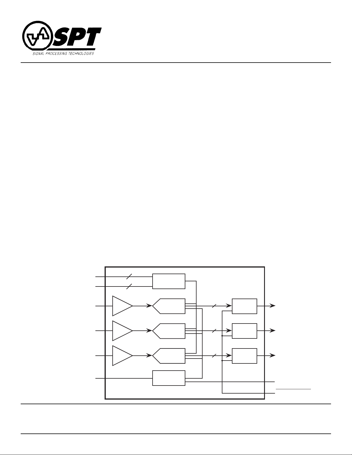
BLOCK DIAGRAM
V
Force/Sense
RH
VRL Force/Sense
Signal Processing Technologies, Inc.
Phone: (719) 528-2300 FAX: (719) 528-2370 Website: http://www.spt.com E-Mail: sales@spt.com
V
IN
VINB
VINC
Clock
2
2
A
T/H
T/H
T/H
4755 Forge Road, Colorado Springs, Colorado 80907, USA
Reference
Ladder
ADC
A
ADC
B
ADC
C
Timing
Generation
10
10
10
Output
Buffer
Output
Buffer
Output
Buffer
DA0–9
DB0–9
DC0–9
DAV
Output Enable
Page 2

ABSOLUTE MAXIMUM RATINGS (Beyond which damage may occur)1 25 °C
Supply Voltages
V
.................................................................................................... +6 V
DD
OV
................................................................................................. +6 V
DD
Temperature
Analog Inputs..................................–0.5 V to VDD +0.5 V
V
................................................–0.5 V to VDD +0.5 V
REF
Clock Input...................................... –0.5 V to VDD +0.5 V
Note: 1. Operation at any Absolute Maximum Rating is not implied and operation beyond the ratings may cause damage to the device.
See Electrical Specifications for proper nominal applied conditions in typical applications.
Output Currents
Digital Outputs .......................................................10 mA
Temperature
Operating Temperature ................................ 0 to + 70 °C
Junction Temperature ......................................... +150 °C
Lead, Soldering (10 seconds)............................. +300 °C
Storage .................................................... –65 to +150 °C
ELECTRICAL SPECIFICATIONS
TA=T
PARAMETERS CONDITIONS LEVEL MIN TYP MAX UNITS
DC Performance
Analog Input
Timing Characteristics
Dynamic Performance
MIN
to T
, VDD=OVDD=+5.0 V, VIN=0 to 4 V, ƒS=30 MSPS, ƒ
MAX
=60 MHz, V
CLK
=4.0 V, V
RHS
=0.0 V, unless otherwise specified.
RLS
TEST TEST SPT7853
Resolution 10 Bits
Differential Linearity ƒs = 20 MSPS V ±0.5 LSB
Integral Linearity ƒs = 20 MSPS V ±1.0 LSB
Input Voltage Range
2
IV V
RLS
V
RHS
V
Input Resistance IV 50 kΩ
Input Capacitance V 5 pF
Input Bandwidth (Full Power) V 120 MHz
–Full-Scale Error
+Full-Scale Error
2
2
V ±0.5 %FS
V ±0.25 %FS
Reference Ladder Resistance VI 120 170 220 Ω
Conversion Rate VI 30 MSPS
Clock Duty Cycle Range IV 45 55 %
Clock-to-Sample Rate Relationship IV 2:1
Pipeline Delay (Latency) IV 12 Clock Cycles
Aperture Delay Time V 5 ns
Aperture Jitter Time V 15 ps
Effective Number of Bits
ƒ
= 3.58 MHz @ 25 °C VI 8.3 8.7 Bits
IN
@ 0 to 70 °C V 8.0 Bits
ƒIN = 10.0 MHz @ 25 °C V 7.4 Bits
Signal-to-Noise Ratio
ƒ
= 3.58 MHz @ 25 °CVI5356dB
IN
@ 0 to 70 °C V 51.6 dB
ƒIN = 10.0 MHz @ 25 °C V 48 dB
Total Harmonic Distortion
ƒIN = 3.58 MHz @ 25 °C VI –56 –58 dB
@ 0 to 70 °C V –54.6 dB
ƒIN = 10.0 MHz @ 25 °C V –51 dB
Signal-to-Noise + Distortion Ratio
ƒIN = 3.58 MHz @ 25 °C VI 52 54.5 dB
@ 0 to 70 °C V 49.7 dB
ƒIN = 10.0 MHz @ 25 °C V 46 dB
2
The full-scale range spans the reference ladder sense pins, V
SPT
RHS
and V
. Refer to the Voltage Reference section for discussion.
RLS
2 12/14/99
SPT7853
Page 3

ELECTRICAL SPECIFICATIONS
TA=T
PARAMETERS CONDITIONS LEVEL MIN TYP MAX UNITS
Dynamic Performance
Power Supply Requirements
Digital Inputs/Outputs
to T
MIN
Spurious Free Dynamic Range
= 3.58 MHz @ 25 °C V 65 dBc
ƒ
IN
Channel-to-Channel Cross Talk
ƒIN = 3.58 MHz V –66 dB
Channel-to-Channel Gain Matching V ±0.1 dB
Differential Phase V 0.5 Degree
Differential Gain V 0.5 %
V
Supply Voltage IV +4.75 +5.0 +5.25 V
DD
OVDD Supply Voltage IV +2.7 +5.25 V
Supply Current
I
DD
OI
DD
Power Dissipation
Without reference ladder CL = 10 pF V 485 mW
Including reference ladder CL = 10 pF VI 580 750 mW
Digital Input Logic 1 Voltage VI 4.0 V
Digital Input Logic 0 Voltage VI 1.0 V
Digital Output Logic 1 Voltage I
Digital Output Logic 0 Voltage IOL = 800 µA VI 0.4 V
t
RISE/tFALL (CL
OEN to Data Output V 12 ns
, VDD=OVDD=+5.0 V, VIN=0 to 4 V, ƒS=30 MSPS, ƒ
MAX
TEST TEST SPT7853
@ 0 to 70 °C V 56.3 dBc
= 500 µAVIOV
OH
= 10 pF) V 10 ns
=60 MHz, V
CLK
VI 81 105 mA
V911mA
=4.0 V, V
RHS
–0.5 V
DD
=0.0 V, unless otherwise specified.
RLS
TEST LEVEL CODES
All electrical characteristics are subject to the
following conditions:
All parameters having min/max specifications
are guaranteed. The Test Level column indicates the specific device testing actually performed during production and Quality Assurance inspection. Any blank section in the data
column indicates that the specification is not
tested at the specified condition.
TEST LEVEL
I
II
III
IV
V
VI
TEST PROCEDURE
100% production tested at the specified temperature.
100% production tested at TA = +25 °C, and sample
tested at the specified temperatures.
QA sample tested only at the specified temperatures.
Parameter is guaranteed (but not tested) by design and
characterization data.
Parameter is a typical value for information purposes
only.
100% production tested at TA = +25 °C. Parameter is
guaranteed over specified temperature range.
SPT
SPT7853
3 12/14/99
Page 4

Figure 1a – Timing Diagram 1
1234567891011121314151617
ANALOG IN
CLOCK IN
SAMPLING CLOCK
(Internal)
VALIDINVALID
DIGITAL OUT
DATA V ALID
Figure 1b – Timing Diagram 2
t
CH
t
CLOCK
IN
t
OD
DATA
DATA
Data 0
t
S
OUTPUT
DA, DB, DC
VALID
CLK
4
5 6 71 2 3 8 9 10 11
t
C
t
CL
Data 1 Data 2
t
DAV
t
DAV
Table I – Timing Parameters
Description Parameters Min Typ Max Units
Conversion time t
Clock period t
C
CLK
Clock duty cycle 45 50 55 %
Clock to output delay (15 pF load) t
DAV pulse width t
Clock to DAV t
OD
DAV
D
SPT
2 x t
CLK
16.67 nS
19 nS
t
CLK
6.5 nS
4 12/14/99
nS
nS
SPT7853
Page 5

TYPICAL PERFORMANCE CHARACTERISTICS
THD, SNR, SINAD vs Input Frequency
65
THD
60
55
SNR
50
45
SINAD
THD, SNR, SINAD (dB)
40
35
02 6 810
4
Input Frequency (MHz)
THD, SNR, SFDR, SINAD vs Temperature
70
65
SFDR
THD, SNR, SINAD vs Sample Rate
80
ƒIN=3.58 MHz
70
THD
60
SNR
50
40
THD, SNR, SINAD (dB)
30
20
010203040
Sample Rate (MSPS)
Power Dissipation vs Sample Rate
600
500
SINAD
1
60
THD
SNR
55
SINAD
50
45
THD, SNR, SFDR, SINAD (dB)
40
020406080
Temperature (°C)
Spectral Response
0
–20
–40
–60
–80
Amplitude (dB)
–100
CLK 30 MHz
ƒIN=3.58 MHz
400
300
200
Power Dissipation (mW)
100
0
0 5 10 15 20
Sample Rate (MSPS)
Note 1: Power dissipation does not include reference.
Large Signal Bandwidth
1.0
0.5
0
–0.5
–1.0
dB
–1.5
–2.0
–2.5
25 30 35 40
–120
0 5 10 15
SPT
Frequency (MHz)
x10
–3.0
0 25 50 75 100 125
6
Frequency (MHz)
5 12/14/99
SPT7853
Page 6

TYPICAL INTERFACE CIRCUIT
Very few external components are required to achieve the
stated device performance. Figure 2 shows the typical interface requirements when using the SPT7853 in normal circuit operation. The following sections provide descriptions
of the major functions and outline critical performance criteria to consider for achieving the optimal device performance.
Figure 2 – Typical Interface Circuit
OV
V
OEN
DAV
CLK
DD
DGND
Hi-Z
+D2.7V–5V
Enable
10
10
10
DD
+D2.7V-5V DGND
Clock
Input
Logic
Interfacing
AGND
Ferrite Bead
REF IN
(+4V typ)
NOTES:
1. Place the Ferrite bead as close to the ADC as possible.
2. All capacitors are 0.01 microfarad surface mount unless otherwise specified.
3. Place 0.01 microfarad surface mount as close to the respective decoupling pin as possible.
4. All input pins (references, analog inputs, clock input and /OEN) must be protected to
within the specified absolute maximum ratings.
VIN1
V
V
4.7
+
2
IN
3
IN
V
RHF
V
RHS
V
RLF
V
RLS
V
RLT
V
CAL
VINA
VINB
VINC
AGND
DGND
AGND
DA0–9
DB0–9
DC0–9
SPT7853
+
4.7
+A5
POWER SUPPLIES AND GROUNDING
The digital and the analog supply voltages on the SPT7853
are internally derived from a single analog supply. A separate digital supply must be used for all interface circuitry
(OVDD). Connect the digital ground (DGND) to the analog
ground plane, as shown in figure 2, to prevent possible
latch-up condition.
OPERATING DESCRIPTION
The general architecture for the CMOS ADC is shown in the
block diagram. Each ADC uses a parallel SAR architecture.
Each contains eight identical successive approximation
ADC sections, all operating in parallel, a 16-phase clock
generator, an 11-bit 8:1 digital output multiplexer, correction logic, and a voltage reference generator which provides common reference levels for each ADC section.
The high sample rate is achieved by using multiple SAR
ADC sections in parallel, each of which samples the input
signal in sequence. Each SAR ADC uses 16 clock cycles to
complete a conversion. The clock cycles are allocated as
follows:
Table II – Clock Cycles
Clock Operation
1 Reference zero sampling
2 Auto-zero comparison
3 Auto-calibrate comparison
4 Input sample
5-15 11-bit SAR conversion
16 Data transfer
The 16-phase clock, which is derived from the input clock,
synchronizes these events. The timing signals for adjacent
ADC sections are shifted by two clock cycles so that the
analog input is sampled on every other cycle of the input
clock by exactly one ADC section. After 16 clock periods,
the timing cycle repeats. The sample rate for the configuration is one-half of the clock rate, e.g., for a 60 MHz clock
rate, the input sample rate is 30 MHz. The latency from analog input sample to the corresponding digital output is 12
clock cycles.
• Since only eight comparators are used, a huge power
savings is realized.
• The auto-zero operation is done using a closed loop system that uses multiple samples of the comparator’s
response to a reference zero.
• The auto-calibrate operation, which calibrates the gain of
the MSB reference and the LSB reference, is also done
with a closed loop system. Multiple samples of the gain
error are integrated to produce a calibration voltage for
each ADC section.
• Capacitive displacement currents, which can induce sampling error, are minimized since only one comparator
samples the input during a clock cycle.
• The total input capacitance is very low since sections of
the converter which are not sampling the signal are isolated from the input by transmission gates.
VOLTAGE REFERENCE
The SPT7853 requires the use of a single external voltage
reference for driving the high side of the reference ladder of
each ADC. It must be within the range of 3 V to 5 V. The
lower side of the ladder is typically tied to AGND (0.0 V), but
can be run up to 2.0 V with a second reference. The analog
input voltage range will track the total voltage difference
measured between the ladder sense lines, V
RHS
and V
RLS
.
SPT
SPT7853
6 12/14/99
Page 7

Force and sense taps are provided to ensure accurate and
stable setting of the upper and lower ladder sense line voltages across part-to-part and temperature variations. By
using the configuration shown in figure 3, offset and gain
errors of less than ±2 LSB can be obtained.
Figure 3 – Ladder Force/Sense Circuit
+
–
–
+
V
RHF
V
RHS
V
RLS
V
RLF
All capacitors are 0.01 µF
Figure 4 – Simplified Reference Ladder Drive Circuit
without Force/Sense Circuit
+4.0 V
External
Reference
(+3.72 V)
V
RHS
280 mV
R/2
R
R
The reference ladder circuit shown in figure 4 is a simplified
representation of the actual reference ladder with force and
sense taps shown. Due to the actual internal structure of the
ladder, the voltage drop from V
to the voltage drop from V
RLF
Typically, the top side voltage drop for V
RHF
to V
to V
RLS
is not equivalent
RHS
.
to V
RHF
RHS
will
equal:
V
– V
RHF
and the bottom side voltage drop for V
V
– V
RLS
= 7% of (V
RHS
= 8.8% of (V
RLF
RHF
– V
RHF
RLF
– V
) (typical),
to V
RLS
) (typical).
RLF
will equal:
RLF
Figure 4 shows an example of expected voltage drops for a
specific case. V
tied to AGND. A 280 mV drop is seen at V
a 350 mV increase is seen at V
of 4.0 V is applied to V
REF
RLS
RHF
RHS
(= 0.35 V).
, and V
RLF
is
(= 3.72 V) and
ANALOG INPUT
The input voltage range is from V
proportionally with respect to the voltage reference. (See
voltage reference section.)
The drive requirements for the analog inputs are very minimal when compared to most other converters, due to the
SPT7853’s extremely low input capacitance of only 5 pF
and very high input resistance of 50 kΩ.
The analog input should be protected through a series resistor and diode clamping circuit as shown in figure 5.
Figure 5 – Recommended Input Protection Circuit
+V
RLS
to V
and will scale
RHS
AV
DD
V
RLF
V
(0.35 V)
(AGND)
(0.0 V)
RLS
350 mV
R
R
R
R
R/2
R=30 Ω (typ)
All capacitors are 0.01 µF
In cases where wider variations in offset and gain can be
tolerated, V
be tied directly to V
can be tied directly to V
REF
as shown in figure 4. Decouple force
RLF
and AGND can
RHF
and sense lines to AGND with a 0.01 µF capacitor (chip cap
preferred) to minimize high-frequency noise injection. If this
simplified configuration is used, the following considerations
should be taken into account:
SPT
D1
ADCBuffer
47 Ω
D2
–V
D1 = D2 = Hewlett Packard HP5712 or equivalent
SPT7853
7 12/14/99
Page 8

CALIBRATION
CLOCK INPUT
The SPT7853 uses an auto-calibration scheme to ensure
10-bit accuracy over time and temperature. Gain and offset
errors are continually adjusted to 10-bit accuracy during
device operation. This process is completely transparent to
the user.
Upon powerup, the SPT7853 begins its calibration algorithm. In order to achieve the calibration accuracy required,
the offset and gain adjustment step size is a fraction of a
10-bit LSB. Since the calibration algorithm is an oversampling process, a minimum of 10k clock cycles are required. This results in a minimum calibration time upon
powerup of 150 µsec. Once calibrated, the SPT7853
remains calibrated over time and temperature.
Since the calibration cycles are initiated on the rising edge
of the clock, the clock must be continuously applied for the
SPT7853 to remain in calibration.
INPUT PROTECTION
All I/O pads are protected with an on-chip protection circuit
shown in figure 6. This circuit provides ESD robustness to
3.5 kV and prevents latch-up under severe discharge conditions without degrading analog transition times.
Figure 6 – On-Chip Protection Circuit
V
DD
120 Ω
Analog
The SPT7853 is driven from a single-ended input clock. Because the pipelined architecture operates on the rising edge
of the clock input, the device can operate over a wide range
of input clock duty cycles without degrading the dynamic
performance. The device’s sample rate is 1/2 of the input
clock frequency. (See the timing diagram.)
DIGITAL OUTPUTS
The digital outputs for each channel (D0–D9) are driven by a
separate supply (OVDD) ranging from +3 V to +5 V. This
feature makes it possible to drive the SPT7853’s CMOScompatible outputs with the user’s logic system supply. The
format of the output data (D0–D9) is straight binary. (See
table III.) The outputs are latched on the rising edge of CLK.
These outputs can be switched into a tri-state mode by
bringing OEN high.
Table III – Output Data Information
ANALOG INPUT OUTPUT CODE
D9-D0
+F.S. + 1/2 LSB 11 1111 1111
+F.S. –1/2 LSB 11 1111 111Ø
+1/2 F.S. ØØ ØØØØ ØØØØ
+1/2 LSB 00 0000 000Ø
0.0 V 00 0000 0000
(Ø indicates the flickering bit between logic 0 and 1).
120 Ω
Pad
POWER SUPPLY SEQUENCING
CONSIDERATIONS
All logic inputs should be held low until power to the device
has settled to the specific tolerances. Avoid power
decoupling networks with large time constants which could
delay VDD power to the device.
DATA AVAILABLE
The Data Available pin goes high when the data output bits
are valid (see figure 1b). Note: Optimal performance of the
data valid pin is achieved when using an input clock with a
minimum span range of ≤1 V (clock low) to ≥4 V (clock high).
EVALUATION BOARD
The EB7853 Evaluation Board is available to aid designers
in demonstrating the full performance of the SPT7853. This
board includes a reference circuit, clock driver circuit, output
data latches and an on-board reconstruction of the digital
data. An application note (AN7853) describing the operation
of this board as well as information on the testing of the
SPT7853 is also available. Contact the factory for price and
availability.
SPT
SPT7853
8 12/14/99
Page 9

PACKAGE OUTLINE
52-Lead TQFP
E
C D
A
B
52
40
SYMBOL MIN MAX MIN MAX
INCHES MILLIMETERS
A 0.472 typ 12.0 typ
1
39
B 0.394 typ 10.0 typ
C 0.472 typ 12.0 typ
D 0.394 typ 10.0 typ
E 0.0630 typ 1.60
F 0.0256 typ 0.65 typ
13
27
G 0.009 0.013 0.22 0.33
H 0.0394 typ 1.0 typ
H
14
26
J
I
I 0.004 0.006 0.09 0.16
J 0.018 0.029 0.45 0.75
K0° 7° 0° 7°
K
F G
SPT
SPT7853
9 12/14/99
Page 10

PIN ASSIGNMENTS
RHF
AGND
DA9
V
RHS
V
RLF
V
RLS
V
RLT
AGND
VINA
AGND
VINB
V
DD
V
CAL
AGND
VINC
AGND
V
52
1
2
3
4
5
6
7
8
9
10
11
12
13
14
N/C
51
15
OEN
50
16
DC0
DA8
49
17
DC1
DA7
48
18
DC2
DA6
47
19
DC3
DA5
46
20
DC4
DA4
45
21
DC5
DA3
44
22
DC6
DA2
43
23
DC7
DA1
42
24
DC8
DA0
41
25
DC9
DGND
40
26
DD
V
PIN FUNCTIONS
Name Function
VINA Analog input for channel A
VINB Analog input for channel B
CLK
39
DB9
38
DB8
37
DB7
36
DB6
35
DB5
34
DB4
33
DB3
32
DB2
31
DB1
30
DB0
29
DAV
28
OV
27
DD
VINC Analog input for channel C
DA0–DA9 CMOS-compatible digital output data for channel A
(+2.7 V to +5.0 voltage logic)
DB0–DB9 CMOS-compatible digital output data for channel B
(+2.7 V to +5.0 voltage logic)
DC0–DC9 CMOS-compatible digital output data for channel C
(+2.7 V to +5.0 voltage logic)
OEN Output enable pin. (Low = enabled; High = high
impedance)
CLK CMOS-compatible input clock (2x of sample rate).
V
V
V
V
V
OV
RHF
RHS
RLF
RLS
DD
DD
Input for top of reference ladder (force)
Input for top of reference ladder (sense)
Input for bottom of reference ladder (force)
Input for bottom of reference ladder (sense)
Analog +5 V; Digital +5 V
Output supply +2.7 / +5 V
AGND Analog ground
DGND Digital ground
V
RLT
V
CAL
Tie to V
RLS
Calibration reference
DAV Data available
ORDERING INFORMATION
PART NUMBER TEMPERATURE RANGE PACKAGE TYPE
SPT7853SCT 0 to +70 °C 52-Pin TQFP
Signal Processing Technologies, Inc. reserves the right to change products and specifications without notice. Permission is hereby expressly
granted to copy this literature for informational purposes only. Copying this material for any other use is strictly prohibited.
WARNING – LIFE SUPPORT APPLICATIONS POLICY – SPT products should not be used within Life Support Systems without the specific
written consent of SPT. A Life Support System is a product or system intended to support or sustain life which, if it fails, can be reasonably
expected to result in significant personal injury or death.
Signal Processing Technologies believes that ultrasonic cleaning of its products may damage the wire bonding, leading to device
failure. It is therefore not recommended, and exposure of a device to such a process will void the product warranty.
SPT7853
SPT
10 12/14/99
 Loading...