

Page 1
SPT7852
DUAL 10-BIT, 20 MSPS, 160 mW A/D CONVERTER
FEATURES
• Dual 10-Bit/20 MSPS Analog-to-Digital Converter
• Monolithic CMOS
• Internal Track-and-Hold
• Low Power Dissipation: 160 mW
• 4 Vp-p Analog Input Range for Each ADC
• Single +5 Volt Power Supply
with Option for 3.3 V Digital Outputs
• Tri-State, TTL-Compatible Outputs
• Overrange Bit
• Selectable Two’s Complement or Straight Binary Output
GENERAL DESCRIPTION
The SPT7852 has two 10-Bit CMOS analog-to-digital converters that can sample data at speeds up to 20 MSPS. It
has excellent low noise performance with a very low typical
power dissipation of only 160 mW—that’s the total power
for
both
converters. The SPT7852 uses a dual configuration
of the proprietary circuit design found in our 10-bit CMOS
single converter family, to achieve its high performance in a
CMOS process.
The SPT7852 is specifically designed for video decoding
applications and is ideal for S-video decoding and decoding
of multiple composite video sources. It is the ADC for the
APPLICATIONS
• SPT NTSC/PAL Video Chip Set
• Video Set-Top Boxes
• Cellular Base Stations
• QPSK/QAM RF Demodulation
• S-Video Digitizers
• Composite Video Digitizers
• Portable and Handheld Instrumentation
SPT NTSC/PAL video decoder chip set that includes the
SPT9210 analog video processor and the SPT2110 video
decoder. It also has excellent application in the area of
coherent I/Q demodulation in such applications as QAM
demodulation and TV set-top box converters.
Inputs and outputs are TTL/CMOS-compatible to interface
with TTL/CMOS-logic systems. Output data format is selectable for either straight binary or two’s complement. The
SPT7852 is available in a 44L TQFP package in commercial
and industrial temperature ranges. It is also available in die
form. For availability of extended temperature ranges,
please contact the factory.
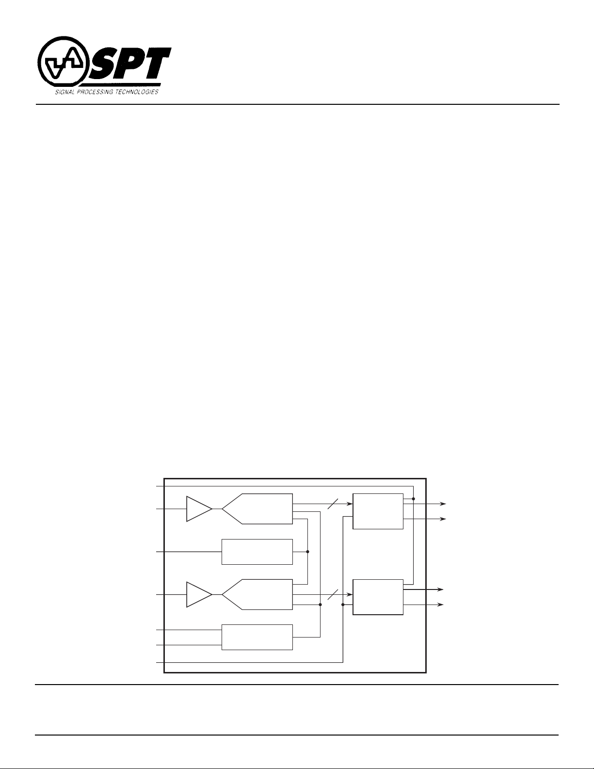
BLOCK DIAGRAM
Reference In
Signal Processing Technologies, Inc.
Phone: (719) 528-2300 FAX: (719) 528-2370 Website: http://www.spt.com E-Mail: sales@spt.com
MSB
Invert
V
INA
V
INB
Clock
Reset
Output
Enable
10
T/H
T/H
ADC
Reference
Ladder
ADC
Timing
Generation
A
B
10
Output
Buffer
Output
Buffer
4755 Forge Road, Colorado Springs, Colorado 80907, USA
Overrange
D
A0-9
Overrange
D
B0-9
Page 2

ABSOLUTE MAXIMUM RATINGS (Beyond which damage may occur)1 25 °C
Supply Voltages
AVDD.........................................................................+6 V
Output
Digital Outputs .......................................................10 mA
DVDD.........................................................................+6 V
Temperature
Input Voltages
Analog Input................................. –0.5 V to AVDD +0.5 V
V
.............................................. –1.5 V to AVDD +0.8 V
Ref
CLK Input ...................................................................V
AV
– DVDD......................................................±100 mV
DD
DD
Operating Temperature ...................................0 to 70 °C
Junction Temperature ........................................... 175 °C
Lead Temperature, (soldering 10 seconds).......... 300 °C
Storage Temperature............................... –65 to +150 °C
Note: 1. Operation at any Absolute Maximum Rating is not implied. See Electrical Specifications for proper nominal
applied conditions in typical applications.
ELECTRICAL SPECIFICATIONS FOR EACH CHANNEL
TA = T
PARAMETERS CONDITIONS LEVEL MIN TYP MAX UNITS
Resolution 10 Bits
DC Accuracy
Analog Input
Reference Input
Conversion Characteristics
Dynamic Performance
MIN
to T
, AVDD = DVDD = +5.0 V, V
MAX
=0 to 4 V, ƒS =20 MSPS, ƒ
IN
=40 MHz, V
CLK
RHS
=4.0 V, V
=0.0 V, unless otherwise specified.
RLS
TEST TEST
Integral Nonlinearity IV ±1.0 LSB
Differential Nonlinearity IV ±1.0 LSB
Input Voltage Range V V
RLS
V
RHS
V
Input Resistance V 50 kΩ
Input Capacitance V 5.0 pF
Input Bandwidth Full Power V 35 MHz
Offset VI ±2.0 LSB
Gain Error VI ±2.0 LSB
Resistance V
RHS
– V
RLS
VI 350 425 500 Ω
Voltage Range
V
RLS
V
RHS
V
– V
∆(V
∆(V
RHS
RHF
RLS
RLS
– V
– V
) V 150 mV
RHS
) V 150 mV
RLF
Maximum Conversion Rate
Minimum Conversion Rate
1
1
IV 0 - 2.0 V
IV 3.0 - AV
DD
V
V 1.0 4.0 5.0 V
VI 20 MHz
IV 100 kHz
Pipeline Delay (Latency) IV 12 Clock Cycles
Aperture Delay Time V 5 ns
Aperture Jitter Time V 15 ps
Effective Number of Bits
ƒ
=3.58 MHz VI 8.4 8.9 Bits
IN
ƒIN= 10 MHz VI 7.9 8.4 Bits
1
2X Clock required.
SPT
SPT7852
2 1/12/00
Page 3

ELECTRICAL SPECIFICATIONS
TA=T
MIN
to T
, AVDD = DVDD = +5.0 V, V
MAX
=0 to 4 V, ƒS =20 MSPS, ƒ
IN
=40 MHz, V
CLK
RHS
= 4.0 V, V
=0.0 V, unless otherwise specified.
RLS
TEST TEST
PARAMETERS CONDITIONS LEVEL MIN TYP MAX UNITS
Dynamic Performance
Signal-to-Noise Ratio
(without Harmonics)
=3.58 MHz VI 53 57 dB
ƒ
IN
ƒIN=10 MHz VI 52 56 dB
Harmonic Distortion
ƒIN=3.58 MHz VI 56 59 dB
ƒIN=10 MHz VI 52 54 dB
Signal-to-Noise and Distortion
(SINAD)
ƒIN=3.58 MHz VI 52 55 dB
ƒIN=10 MHz VI 49 52 dB
Channel-to-Channel Crosstalk ƒIN=3.58 MHz IV 70 dB
Channel-to-Channel Gain Matching Full Scale IV 0.04 dB
Spurious Free Dynamic Range ƒIN=3.58 MHz @ –3 dB FS V 66 dB
Differential Phase V 0.2 Degree
Differential Gain V 0.3 %
Digital Inputs
Logic "1" Voltage VI 2.0 V
Logic "0" Voltage VI 0.8 V
Maximum Input Current Low V
=0 V VI –10 +10 µA
IL
Maximum Input Current High VIH=5 V VI –10 +10 µA
Input Capacitance V 5 pF
Digital Outputs
Logic "1" Voltage IOH=0.5 mA VI OVDD–0.5 V
Logic "0" Voltage IOS=1.6 mA VI 0.4 V
t
RISE/tFALL
15 pF Load V 10 ns
Output Enable to Data Output Delay 20 pF Load, TA=+25 °C V 10 ns
50 pF Load Over Temp. V 22 ns
Power Supply Requirements
Voltages DV
AV
OV
Currents AI
DI
DD
DD
DD
DD
DD
Total for Both Converter VI 15 18 mA
Channels VI 17 20 mA
IV 4.75 5.0 5.25 V
IV 4.75 5.0 5.25 V
IV 2.7 5.0 5.25 V
Power Dissipation VI 160 190 mW
TEST LEVEL CODES
All electrical characteristics are subject to the following conditions:
All parameters having min/max specifications are
guaranteed. The Test Level column indicates the
specific device testing actually performed during
production and Quality Assurance inspection. Any
blank section in the data column indicates that the
specification is not tested at the specified condition.
SPT
TEST LEVEL
I
II
III
IV
V
VI
TEST PROCEDURE
100% production tested at the specified temperature.
100% production tested at T
=+25 °C, and sample tested at
A
the specified temperatures.
QA sample tested only at the specified temperatures.
Parameter is guaranteed (but not tested) by design and char-
acterization data.
Parameter is a typical value for information purposes only.
100% production tested at T
= +25 °C. Parameter is guaran-
A
teed over specified temperature range.
SPT7852
3 1/12/00
Page 4
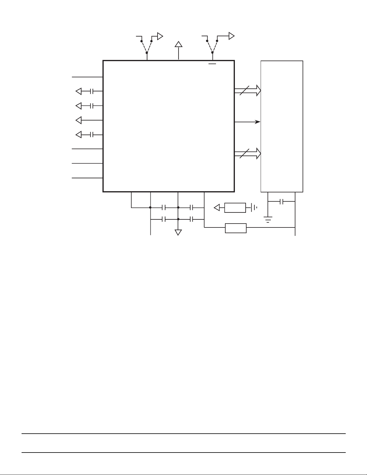
Figure 1 –Typical Interface Circuit
+A5
+A5
3-st
EN
Ref In
(+4 V)
V
IN1
V
IN2
Clock
V
RHF
V
RHS
V
RLS
V
RLF
V
CAL
V
INA
V
INB
CLK
MSBINV Reset
SPT7852
AV
DD
DV
DD
.1 µF .1 µF
4.7 µF 4.7 µF
+A5
GND OV
EN
Digital
Output A
DAV
Digital
Output B
DD
11
Interfacing
Logic
11
FB
*
FB
*
3.3 V/5 V
1. Place the ferrite bead (*) as close to the ADC as possible.
2. Place 0.1 µF decoupling capacitors as close to the ADC as possible.
3. All capacitors are 0.1 µF surface-mount unless otherwise specified.
4. All analog input pins (references, analog input, clock input) must
be protected. (See absolute maximum ratings.)
TYPICAL INTERFACE CIRCUIT
Very few external components are required to achieve the
stated device performance. Figure 1 shows the typical interface requirements when using the SPT7852 in normal
circuit operation. The following sections provide descriptions of the major functions and outline critical performance
criteria to consider for achieving the optimal device performance.
POWER SUPPLIES AND GROUNDING
SPT suggests that both the digital and the analog supply
voltages on the SPT7852 be derived from a single analog
supply as shown in figure 1. A separate digital supply must
be used for all interface circuitry. SPT suggests using this
power supply configuration to prevent a possible latch-up
condition on powerup.
SPT
SPT7852
4 1/12/00
Page 5

OPERATING DESCRIPTION
The general architecture for the CMOS ADC is shown in the
block diagram. The design contains two sets of eight identical
successive approximation ADC sections, all operating in parallel, a 16-phase clock generator, an 11-bit 8:1 digital output
multiplexer, correction logic, and a voltage reference generator which provides common reference levels for each ADC
section.
The high sample rate is achieved by using multiple SAR
ADC sections in parallel, each of which samples the input
signal in sequence. Each ADC uses 16 clock cycles to
complete a conversion. The clock cycles are allocated as
follows:
Table I – Clock Cycles
Clock Operation
1 Reference zero sampling
2 Auto-zero comparison
3 Auto-calibrate comparison
4 Input sample
5–15 11-bit SAR conversion
16 Data transfer
The 16-phase clock, which is derived from the input clock,
synchronizes these events. The timing signals for adjacent
ADC sections are shifted by two clock cycles so that the
analog input is sampled on every other cycle of the input
clock by exactly one ADC section. After 16 clock periods,
the timing cycle repeats. The sample rate for the configuration is one-half of the clock rate, e.g., for a 40 MHz clock
rate, the input sample rate is 20 MHz. The latency from analog input sample to the corresponding digital output is 12
clock cycles.
• Since only sixteen comparators are used, a huge power
savings is realized.
• The auto-zero operation is done using a closed loop system that uses multiple samples of the comparator's response to a reference zero.
• The auto-calibrate operation, which calibrates the gain of
the MSB reference and the LSB reference, is also done
with a closed loop system. Multiple samples of the gain
error are integrated to produce a calibration voltage for
each ADC section.
• Capacitive displacement currents, which can induce sampling error, are minimized since only one comparator per
VIN input samples the input during a clock cycle.
• The total input capacitance is very low since sections of
the converter which are not sampling the signal are isolated from the input by transmission gates.
SPT
SPT7852
5 1/12/00
Page 6

Figure 2 – Timing Diagram 1
Clock
Reset
t
C
t
CLK
2
Data
t
1
d
3
t
Set
Valid (DAV)
t
Data
Output
OD
4
Invalid InvalidInvalid
(Channel A)
t
OD
Data
Output
Invalid InvalidInvalid
(Channel B)
Notes:
1) Data Valid is forced low on Reset = High.
2) Data updated on first rising edge of clock after Reset goes low.
3) Data Valid rising edge will occur on the second rising edge of Clock
after Reset goes low. Use the rising edge of Data Valid to latch the ADC output data.
4) Analog Input Data is sampled during the first clock cycle after Reset goes low.
Valid data output from this sample will be available 12 clock cycles
later (6 Data Valid cycles). All data during the 12 clock cycle latency is invalid.
t
Hold
CLOCK INPUT
The SPT7852 is driven from a single-ended TTL-input
clock. Because the pipelined architecture operates on the
rising edge of the clock input, the device can operate over a
wide range of input clock duty cycles without degrading the
dynamic performance. The device's sample rate is 1/2 of
the input clock frequency. (See timing diagram.)
TIMING AND RESET FUNCTION
The two on-board ADCs in the SPT7852 are driven off of a
single external TTL clock. This external clock must be 2X
the desired sample rate. In applications that require a
known phase relationship between the clock, analog input
sampling and valid data output, a reset function is provided
to establish a known phase relationship. (Because of the 2X
clock, an exact phase relationship will not be known otherwise.) Refer to figure 2, Timing Diagram 1.
SPT
The reset pin is low for normal device operation. When reset
is brought high, Data Valid (DAV) is immediately forced low
and data output updates are suspended. Operation will resume on the first rising edge of the clock after the reset pin
has been brought low. The first Data Valid rising edge will
occur on the second edge of the clock after the reset goes
low.
The first analog input sample will be taken during the first
clock cycle after reset goes low. Valid data from this
sample will be available 12 clock cycles later. All data during this 12 cycle latency will be invalid (Refer to figure 3,
Timing Diagram 2.)
SPT7852
6 1/12/00
Page 7

Figure 3 – Timing Diagram 2
Analog In
(Channel A)
Analog In
(Channel B)
Clock In
Reset
Sampling Clock
(Internal)
Data Out
(Channel A)
Data Out
(Channel B)
Data V alid
1
2
4
3
6
5
7
8
9
10
11
Invalid Valid
1234
Invalid Valid
1234
Table II – Timing Parameters Table
DESCRIPTION PARAMETERS MIN TYP MAX UNITS
Conversion Time t
Clock Period t
Clock Duty Cycle 40 50 60 %
Output Delay
(15 pF Load) t
DAV Pulse Width t
Clock to DAV t
Data Set Up Time t
Data Hold Time t
c
CLK
OD
DAV
d
Set
Hold
2*t
CLK
25 ns
11 ns
t
CLK
15 ns
22
28
ns
ns
SPT
SPT7852
7 1/12/00
Page 8

Figure 4 – Ladder Force/Sense Circuit
Figure 5 – Simplified Reference Ladder Drive Circuit
Without Force/Sense Circuit
+
-
-
+
1
V
RHF
2
V
RHS
3
V
RLS
4
V
RLF
5
AGND
All capacitors are 0.01 µF
VOLTAGE REFERENCE
The SPT7852 requires the use of a single external voltage
reference for driving the high side of the reference ladder. It
must be within the range of 3 V to 5 V. Both ADCs share the
same reference ladder. The lower side of the ladder is typically tied to AGND (0.0 V), but can be run up to 2.0 V with a
second reference. The analog input voltage range will track
the total voltage difference measured between the ladder
sense lines, V
Force and sense taps are provided to ensure accurate and
stable setting of the upper and lower ladder sense line voltages across part-to-part and temperature variations. By using the configuration shown in figure 4, offset and gain errors of less than ±2 LSB can be obtained.
In cases where wider variations in offset and gain can be
tolerated, V
be tied directly to V
and sense lines to AGND with a .01 µF capacitor (chip cap
preferred) to minimize high-frequency noise injection. If this
simplified configuration is used, the following considerations
should be taken into account:
and V
RHS
can be tied directly to V
Ref
RLF
.
RLS
as shown in figure 5. Decouple force
and AGND can
RHF
+4.0 V
External
Reference
V
RHS
(+3.85 V)
V
RLS
(0.150 V)
V
(AGND)
RLF
0.0 V
tied to AGND. A 150 mV drop is seen at V
a 150 mV increase is seen at V
150 mV
150 mV
R/2
R
R
R
R
R
R
R/2
RLS
R=30 Ω (typ)
All capacitors are 0.01 µF
(= 3.85 V) and
RHS
(= 0.150 V).
ANALOG INPUT
V
and V
INA
nel B, respectively. Both channels share the same reference ladder. The input voltage range is from V
(typically 4.0 V) and will scale proportionally with respect to
the voltage reference. (See voltage reference section.)
The drive requirements for the analog inputs are very minimal when compared to most other converters due to the
SPT7852’s extremely low input capacitance of only 5 pF
and very high input resistance of 50 kΩ.
The analog input should be protected through a series resistor and diode clamping circuit as shown in figure 6.
Figure 6 – Recommended Input Protection Circuit
are the analog inputs for channel A and chan-
INB
to V
RLS
+V
AV
DD
RHS
The reference ladder circuit shown in figure 5 is a simplified
representation of the actual reference ladder with force and
sense taps shown. Typically, the top side voltage drop for
V
to V
RHF
V
RHF
and the bottom side voltage drop for V
V
RLS
– V
– V
will equal:
RHS
= 3.75% of (V
RHS
= 3.75% of (V
RLF
RHF
RHF
– V
– V
) (typical),
RLF
to V
RLS
) (typical).
RLF
will equal:
RLF
Figure 5 shows an example of expected voltage drops for a
specific case. V
of 4.0 V is applied to V
Ref
RHF
and V
RLF
is
SPT
D1
ADCBuffer
47 Ω
D2
-V
D1 = D2 = Hewlett Packard HP5712 or equivalent
SPT7852
8 1/12/00
Page 9

CALIBRATION
The SPT7852 uses an auto-calibration scheme to ensure
10-bit accuracy over time and temperature. Gain and offset
errors are continually adjusted to 10-bit accuracy during device operation. This process is completely transparent to the
user.
Upon powerup, the SPT7852 begins its calibration algorithm. In order to achieve the calibration accuracy required,
the offset and gain adjustment step size is a fraction of a 10bit LSB. Since the calibration algorithm is an oversampling
process, a minimum of 10k clock cycles are required. This
results in a minimum calibration time upon powerup of 250
µsec (for a 20 MHz sample rate). Once calibrated, the
SPT7852 remains calibrated over time and temperature.
Since the calibration cycles are initiated on the rising edge
of the clock, the clock must be continuously applied for the
SPT7852 to remain in calibration.
POWER SUPPLY SEQUENCING
CONSIDERATIONS
All logic inputs should be held low until power to the device
has settled to the specific tolerances. Avoid power decoupling networks with large time constants which could delay
VDD power to the device.
DIGITAL OUTPUTS, DATA VALID,
AND MSB INVERT
The output data for both channels can be latched using the
rising edge of Data Valid (DAV). Refer to table II for minimum data setup and hold times. The format of the data is
straight binary when the MSB Invert pin (MSBINV) is held
low and Two’s Complement format when MSB Invert is
high.
OVERRANGE OUTPUT
INPUT PROTECTION
All I/O pads are protected with an on-chip protection circuit
shown in figure 7. This circuit provides ESD robustness to
3.5 kV and prevents latch-up under severe discharge conditions without degrading analog transition times.
Figure 7 – On-Chip Protection Circuit
V
DD
120 Ω
120 Ω
Pad
Analog
An OVERRANGE OUTPUT from D10A or D10B is an indication that the analog input signal has exceeded the positive full-scale input voltage by 1 LSB. When this condition
occurs, D10A/B will switch to logic 1. All other data outputs
(D0A/B to D9A/B) will remain at logic 1 as long as D10A/B
remains at logic 1. This feature makes it possible to include
the SPT7852 in higher resolution systems.
Table III – Output Data Information (Binary Code)
Overrange (MSBINV=0) (MSBINV=1)
Analog Input D10A/B D9A/B–D0A/B D9A/B–D0A/B
+FS + 1/2 LSB 1 11 1111 1111 01 1111 1111
+FS – 1/2 LSB 0 11 1111 111Ø 01 1111 111Ø
[+FS –(–FS)]/2 0 ØØ ØØØØ ØØØØ ØØ ØØØØ ØØØØ
–FS + 1/2 LSB 0 00 0000 000Ø 10 0000 000Ø
–FS 0 00 0000 0000 10 0000 0000
Ø indicates the flickering bit between logic 0 and 1.
+FS = V
; –FS = V
RHS
Output Code Output Code
RLS
SPT
SPT7852
9 1/12/00
Page 10

PACKAGE OUTLINE
44-LEAD TQFP
A
B
Pin 1
G
Index
E F
C
D
SYMBOL MIN MAX MIN MAX
INCHES MILLIMETERS
A 0.472 Typ 12.00 Typ
B 0.394 Typ 10.00 Typ
C 0.394 Typ 10.00 Typ
D 0.472 Typ 12.00 Typ
E 0.031 Typ 0.80 Typ
F 0.012 0.017 0.300 0.45
G 0.035 0.040 0.85 1.05
H 0.002 0.006 0.05 0.15
I 0.018 0.030 0.450 0.750
J 0.039 Typ 1.00 Typ
K 0-7° 0-7°
H
I
K
J
SPT
SPT7852
10 1/12/00
Page 11

PIN ASSIGNMENTS
PIN FUNCTIONS
V
RHF
V
RHS
V
RLS
V
RLF
GND
V
GND
V
MSBINV
Reset
V
CAL
INA
INB
AV
DD
44
1
2
3
4
5
6
7
8
9
10
11
12
OV
DV
GND
DD
42
43
14
13
EN
DD
40
41
TOP VIEW
16
15
D10
A
D8
D7
D5
D9
A
39
38
17
18
D6
A
A
A
A
37
19
34
36
35
33
32
31
30
29
28
27
26
25
24
23
22
20
21
D4
D3
D2
D1
D0
DAV
D0
D1
D2
D3
D4
NAME FUNCTION
V
RHF
V
RHS
V
RLS
V
A
A
A
A
A
B
B
B
B
B
RLF
V
CAL
V
INA
V
INB
AV
DD
DV
DD
OV
DD
GND Common Device Ground
CLK Input Clock (ƒ
EN
D0A – D9A Channel A Tri-State Data Output
Reference High Force
Reference High Sense
Reference Low Sense
Reference Low Force
Calibration Reference
Channel A Analog Input
Channel B Analog Input
Analog Power Supply
Digital Power Supply
Digital Output Supply (3.3 V/5 V)
= 2 * ƒS)
CLK
Output Enable (Low = Data)
(D0A = LSB)
D0B – D9B Channel B Tri-State Data Output
AV
DD
OV
DV
GND
DD
D10
D9
CLK
DD
D8
B
B
B
D5
D6
D7
B
B
B
D10A Channel A Overrange Bit
(D0B = LSB)
D10B Channel B Overrange Bit
DAV Data Valid Output
MSBINV MSB Invert (High = 2’s complement)
(Low = binary)
Reset Reset (Low = Normal) (High = Reset)
ORDERING INFORMATION
PART NUMBER TEMPERATURE RANGE PACKAGE TYPE
SPT7852SCT 0 to +70 °C 44L TQFP
SPT7852SIT –40 to +85 °C 44L TQFP
SPT7852SCU +25 °C Die*
*Please see the die specification for guaranteed electrical performance.
Signal Processing Technologies, Inc. reserves the right to change products and specifications without notice. Permission is hereby expressly
granted to copy this literature for informational purposes only. Copying this material for any other use is strictly prohibited.
Covered by Patent Numbers 5262779 and 5272481.
WARNING – LIFE SUPPORT APPLICATIONS POLICY – SPT products should not be used within Life Support Systems without the specific
written consent of SPT. A Life Support System is a product or system intended to support or sustain life which, if it fails, can be reasonably
expected to result in significant personal injury or death.
Signal Processing Technologies believes that ultrasonic cleaning of its products may damage the wire bonding, leading to device
failure. It is therefore not recommended, and exposure of a device to such a process will void the product warranty.
SPT7852
SPT
11 1/12/00
 Loading...