

Page 1
SPT7851
10-BIT, 20 MSPS, 79 mW A/D CONVERTER
FEATURES
• 10-Bit, 20 MSPS Analog-to-Digital Converter
• Monolithic CMOS
• Internal Track-and-Hold
• Low Input Capacitance: 1.4 pF
• Low Power Dissipation: 79 mW
• 2.8 – 3.6 V Power Supply Range
• TTL-Compatible Outputs
• –40 °C to +85 °C Operation
GENERAL DESCRIPTION
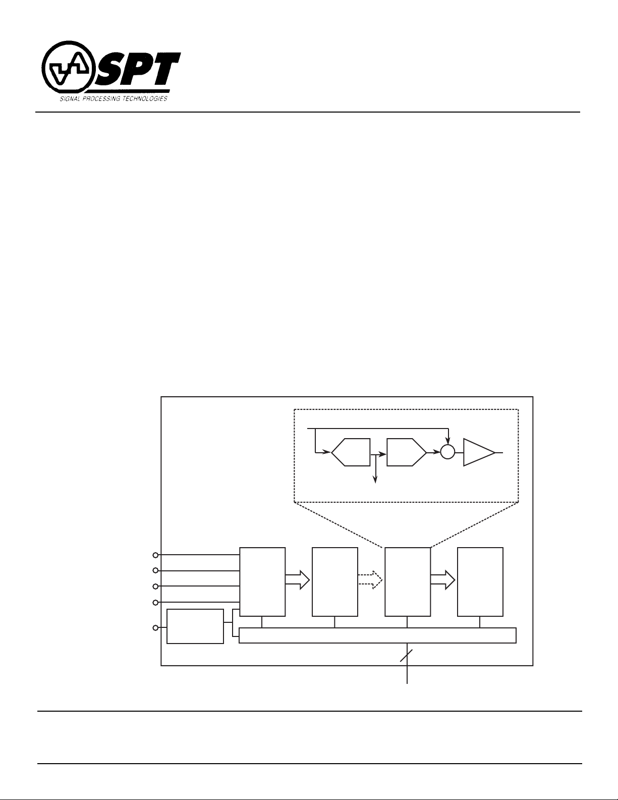
The SPT7851 10-bit, 20 MSPS analog-to-digital converter
has a pipelined converter architecture built in a CMOS process. It delivers high performance with a typical power dissipation of only 79 mW. With low distortion and high dynamic
BLOCK DIAGRAM
APPLICATIONS
• CCD Imaging Cameras and Sensors
• Medical Imaging
• RF Communications
• Document and Film Scanners
• Electro-Optics
• Transient Signal Analysis
• Handheld Equipment
range, this device offers the performance needed for imaging, multimedia, telecommunications and instrumentation
applications.
The SPT7851 is available in a 44-lead Thin Quad Flat Pack
(TQFP) package in the industrial temperature range (–40 °C
to +85 °C).
–
+
G=2
Stage
10
V
V
VIN+
VIN–
REF
REF
CLK
DACADC
D<1…0> Pipeline Stage
+
–
Clock
Driver
Stage
1
Stage
2
Digital Delays, Error Correction and Output
Digital Output (D0 – D9)
Stage
9
10
Signal Processing Technologies, Inc.
4755 Forge Road, Colorado Springs, Colorado 80907, USA
Phone: (719) 528-2300 FAX: (719) 528-2370 Website: http://www.spt.com E-Mail: sales@spt.com
Page 2

ABSOLUTE MAXIMUM RATINGS (Beyond which damage may occur)1 25 °C
Supply Voltages
V
..............................................................................–0.5 V to +6 V
DD
1
V
..............................................................................–0.5 V to +6 V
DD
2
V
..............................................................................–0.5 V to +6 V
DD
3
Temperature
Operating Temperature ............................. –40 to +85 °C
Storage Temperature............................... –65 to +125 °C
Input Voltages
Analog Input................................. –0.5 V to (VDD +0.5 V)
Digital Input .................................. –0.5 V to (VDD +0.5 V)
V
+ ........................................... –0.5 V to (VDD +0.5 V)
REF
V
– ........................................... –0.5 V to (VDD +0.5 V)
REF
CLK .............................................. –0.5 V to (VDD +0.5 V)
Note: 1. Operation at any Absolute Maximum Rating is not implied. See Electrical Specifications for proper nominal
applied conditions in typical applications.
ELECTRICAL SPECIFICATIONS
TA = T
MIN–TMAX
Bias 1 = 90 µA, Bias 2 = 9.5 µA, Differential Input, Duty Cycle = 50%, unless otherwise specified.
PARAMETERS CONDITIONS LEVEL MIN TYP MAX UNITS
DC Accuracy
Resolution 10 Bits
Differential Linearity V ±0.6 LSB
Integral Linearity V ±0.75 LSB
No Missing Codes VI Guaranteed
, V
DD1
= V
DD2
= V
= 3.3 V, V
DD3
– = 1.0 V, V
REF
+ = 2.0 V, Common Mode Voltage = 1.65 V, ƒ
REF
TEST TEST SPT7851
= 20 MSPS,
CLK
Analog Input
Input Voltage Range (Differential) IV ±0.6 ±1.0 ±1.7 V
Common Mode Input Voltage IV 1.2 1.65 1.9 V
Input Capacitance V 1.4 pF
Input Bandwidth (Large Signal) V 120 MHz
Offset (Mid-scale) V
+ = VIN– = V
IN
CM
V ±1.0 % FSR
Gain Error V 0.3 % FSR
Reference Voltages
Reference Input Voltage Range IV 0.6 1.0 1.7 V
(V
+ – V
REF
Negative Reference Voltage (V
Positive Reference Voltage (V
Common Mode Output Voltage (V
+ Current V 35 µA
V
REF
V
– Current V –25 µA
REF
REF
–)
–) IV 0.9 1.0 1.3 V
REF
+) IV 1.9 2.0 2.9 V
REF
)IO = –1 µA VI 1.3 1.65 1.8 V
CM
Switching Performance
Maximum Conversion Rate VI 20 MHz
Pipeline Delay IV 7.5 Clocks
(See Timing Diagram)
Aperture Delay Time (TAP)V5ns
Aperture Jitter Time V 10 ps-rms
SPT
SPT7851
2 8/1/00
Page 3

ELECTRICAL SPECIFICATIONS
TA = T
MIN–TMAX
, V
DD1
= V
DD2
= V
= 3.3 V, V
DD3
– = 1.0 V, V
REF
+ = 2.0 V, Common Mode Voltage = 1.65 V, ƒ
REF
= 20 MSPS,
CLK
Bias 1 = 90 µA, Bias 2 = 9.5 µA, Differential Input, Duty Cycle = 50%, unless otherwise specified.
TEST TEST SPT7851
PARAMETERS CONDITIONS LEVEL MIN TYP MAX UNITS
Dynamic Performance
Effective Number of Bits
ƒIN = 5.0 MHz VI 9.0 9.3 Bits
= 10.0 MHz V 9.0 Bits
ƒ
IN
Signal-To-Noise Ratio
ƒIN = 5.0 MHz VI 57 58 dB
= 10.0 MHz V 58 dB
ƒ
IN
Total Harmonic Distortion
ƒIN=5.0 MHz VI –68 –61 dB
=10.0 MHz V –60 dB
ƒ
IN
Signal-To-Noise and Distortion
ƒIN = 5 MHz VI 56 58 dB
= 10 MHz V 56 dB
ƒ
IN
Spurious Free Dynamic Range
ƒIN = 5.0 MHz VI 62 70 dB
= 10.0 MHz V 61 dB
ƒ
IN
Differential Phase V 0.2 Degrees
Differential Gain V 0.5 %
Digital Inputs
Logic 1 Voltage VI 80% V
Logic 0 Voltage VI 20% V
DD
DD
Maximum Input Current Low VIN = GND VI ±1 µA
Maximum Input Current High V
IN
= V
DD
VI ±1 µA
Input Capacitance V 1.8 pF
Digital Outputs
Logic 1 Voltage I
Logic 0 Voltage I
CLK to Output Delay Time (t
)IV4812ns
D
= –2 mA VI 85% V
O
= +2 mA VI 0.1 0.4 V
O
DD
95% V
DD
Power Supply Requirements
Supply Voltages
V
, V
DD1
DD2
, V
DD3
IV 2.8 3.3 3.6 V
Supply Current
I
DD
VI 24 30 mA
Power Dissipation VI 79 100 mW
Power Supply Rejection Ratio (PSRR) V 67 dB
TEST LEVEL CODES
All electrical characteristics are subject to the
following conditions: All parameters having
min/max specifications are guaranteed. The
Test Level column indicates the specific device
testing actually performed during production
and Quality Assurance inspection. Any blank
section in the data column indicates that the
specification is not tested at the specified condition.
TEST LEVEL
I
II
III
IV
V
VI
TEST PROCEDURE
100% production tested at the specified temperature.
100% production tested at TA = +25 °C, and sample tested
at the specified temperatures.
QA sample tested only at the specified temperatures.
Parameter is guaranteed (but not tested) by design and
characterization data.
Parameter is a typical value for information purposes only.
100% production tested at TA = +25 °C. Parameter is
guaranteed over specified temperature range.
V
SPT
SPT7851
3 8/1/00
Page 4

TYPICAL PERFORMANCE CHARACTERISTICS
)
THD, SNR, SINAD vs Input Frequency
80
70
60
50
40
THD, SNR, SINAD (dB)
30
20
0
10
THD, SNR, SINAD vs Temperature
70
68
66
64
62
60
THD, SNR, SINAD (dB)
58
56
–40 0–25
THD
SNR
SINAD
1
10
Input Frequency (MHz)
Temperature (°C)
25 70
50
THD
SNR
SINAD
THD, SNR, SINAD vs Sample Rate
80
70
THD
60
50
40
SNR
SINAD
THD
SNR
SINAD
THD, SNR, SINAD (dB)
30
20
2
10
0
10
1
10
2
10
Sample Rate (MSPS)
Note: Bias1 and Bias2 currents optimized for each sample rate.
Power Dissipation vs Sample Rate
150
125
100
75
50
Power Dissipation (mW)
25
0
0
85
10
Sample Rate (MSPS)
Note: Bias1 and Bias2 optimized for each sample rate.
1
10
2
10
3.4
3.2
3.0
2.8
2.6
VBias1 (V)
2.4
2.2
2.0
0 30 60 90 120 150 180
SPT
Bias 1 Voltage vs Bias 1 Current
Bias 1 VBias 1
30 2.19
60 2.53
90 2.79
120 3
150 3.22
IBias1 (µA)
Bias 2 Voltage vs Bias 2 Current
0.90
0.85
0.80
IBias 2 VBias 2
0.75
VBias 2 (V)
0.70
3 0.6975
6 0.7535
9 0.796
12 0.8295
15 0.8595
0.65
0.60
0 3 6 9 12 15 18
IBias 2 (µA
SPT7851
4 8/1/00
Page 5

Figure 1 – Timing Diagram
Sampling Points
N-1
N
N+1
t
AP
A
IN
CLK
D
OUT
GENERAL DESCRIPTION
The SPT7851 is an ultra-low power, 10-bit, 20 MSPS ADC.
It has a pipelined architecture and incorporates digital error
correction of all 10 bits. This error correction ensures good
linearity performance for input frequencies up to Nyquist.
The inputs are fully differential, making the device insensitive to system-level noise. This device can also be used in a
single-ended mode. (See analog input section.) With the
power dissipation roughly proportional to the sampling rate,
this device is ideal for very low power applications in the
range of 1 to 20 MSPS.
N+2
t
D
N+6
N+7
N+8
N-2 N-1 N
TYPICAL INTERFACE CIRCUIT
The SPT7851 requires few external components to achieve
the stated operation and performance. Figure 2 shows the
typical interface requirements when using the SPT7851 in
normal circuit operation. The following sections provide a
description of the functions and outline critical performance
criteria to consider for achieving the optimal device performance.
Figure 2 – Typical Interface Circuit
Ref- In
(+1.15 V)
Ref+ In
(+2.15 V)
90 µA
9.5 µA
.01 µF
(+1.65 V)
RF In
51
Minicircuit
T1-6T
4.7 µF
+
68 pF
4.7 µF
.01 µF
12
22
N/C
N/C
N/C
GND
Bias1
Bias2
V
CM
GND
VIN+
VINGND
23
+3.3 V CLK In
.01 µF
+
11
Ref
V
V
V
DD1
Ref
-
+
V
DD1
V
DD1
V
DD2
+
.01 µF
U1
SPT7851
GND
10 µF
V
DD2
AGND
V
DD3
(3 V Logic)
GND
N/C
CLK
V
DNC
DNC
D9
(MSB)
33
DD3
D0
D1
D2
D3
D4
D5
D6
D7
D8
0.1 µF
1
+3.3 V
44
(LSB)
34
FB
+3.3 V Digital
Decoupling Cap
Interfacing
3 V Logic
DGND
SPT
Note: 1. All V
2. FB = Ferrite Bead; must be placed as close to U1 as possible.
DD1
, V
DD2
and V
should be tied together.
DD3
SPT7851
5 8/1/00
Page 6

ANALOG INPUT
REFERENCES
The input of the SPT7851 can be configured in various ways
depending on if a single-ended or differential, AC- or DCcoupled input is desired.
The AC coupled input is most conveniently implemented
using a transformer with a center tapped secondary winding. The center tap is connected to the VCM pin as shown in
figure 2. To obtain low distortion, it is important that the selected transformer does not exhibit core saturation at the
full-scale voltage. Proper termination of the input is important for input signal purity. A small capacitor across the inputs attenuates kickback noise from the internal sample and
hold.
Figure 3 illustrates a solution (based on operational amplifiers) that can be used if a a DC-coupled single-ended input is
desired. The selection criteria of the buffer op-amps is as
follows:
- Open loop gain >75 dB
- Gain bandwidth product >50 MHz
- Total Harmonic Distortion ≤–75 dB
- Signal-to-Noise Ratio >75 dB
Figure 3 – DC-Coupled Single-Ended to Differential
Conversion (power supplies and bypassing
are not shown)
V
CM
Input
Voltage
(±0.5 V)
R3
(R3)/2
R3
–
+
R
R2
R2
R
–
+
51 Ω
15 pF
ADC
VIN+
VIN–
The SPT7851 has a differential analog input. The voltages
applied to the V
voltage range and are equal to ±(V
REF
+ and V
– pins determine the input
REF
REF
+ – V
–). This volt-
REF
age range will be symmetrical about the common mode voltage. Externally generated reference voltages must be connected to these pins. (See figure 2, Typical Interface
Circuit.) For best performance, these voltages should be
symmetrical about the midpoint of the supply voltage.
COMMON MODE VOLTAGE
REFERENCE CIRCUIT
The SPT7851 has an on-board common mode voltage reference circuit (VCM). It is typically one-half of the supply voltage and can drive loads of up to 20 µA. This circuit is commonly used to drive the center tap of the RF transformer in
fully differential applications. For single-ended applications,
this output can be used to provide the level shifting required
for the single-to-differential converter conversion circuit.
BIAS CURRENT CIRCUITS
The bias currents suggested (Bias 1 and Bias 2 in figure 2)
optimize device performance for the stated sample rate of
20 MSPS. To achieve the best dynamic performance when
operating the device at sample rates other than 20 MSPS,
the bias current levels should be adjusted. Table I shows the
settings for Bias 1 and Bias 2 for selected sample rates.
The “Bias Voltage vs Bias Current” graphs on page 4 show
the relationship between the bias current and the bias
voltage. Please refer to the application note for more
information.
51 Ω
R
RR
+
–
51 Ω
POWER SUPPLIES AND GROUNDING
The SPT7851 is operated from a single power supply in the
range of 2.8 to 3.6 volts. Nominal operation is suggested to
be 3.3 volts. All power supply pins should be bypassed as
close to the package as possible. The analog and digital
grounds should be connected together with a ferrite bead as
shown in the typical interface circuit and as close to the ADC
as possible.
SPT
Table I – Sample Rate Settings
Sample Rate (MHz) Bias 1 (µA) Bias 2 (µA)
1 30 3.0
5 50 6.0
10 70 7.5
20 90 9.5
SPT7851
6 8/1/00
Page 7

CLOCK
The SPT7851 accepts a low voltage CMOS logic level at
the CLK input. The duty cycle of the clock should be kept as
close to 50% as possible. Because consecutive stages in
the ADC are clocked in opposite phase to each other, a non50% duty cycle reduces the settling time available for every
other stage and thus could potentially cause a degradation
of dynamic performance.
For optimal performance at high input frequencies, the clock
should have low jitter and fast edges. The rise/fall times
should be kept shorter than 2 ns. Overshoot and undershoot
should be avoided. Clock jitter causes the noise floor to rise
proportional to the input frequency. Because jitter can be
caused by crosstalk on the PC board, it is recommended
that the clock trace be kept as short as possible and standard transmission line practices be followed.
DIGITAL OUTPUTS
The digital output data appears in an offset binary code at
3.3 V CMOS logic levels. A negative full scale input results
in an all zeros output code (000…0). A positive full scale
input results in an all 1’s code (111…1). The output data is
available 7.5 clock cycles after the data is sampled. The input signal is sampled on the high to low transition of the
input clock. Output data should be latched on the low to high
clock transition as shown in figure 1, the Timing Diagram.
The output data is invalid for the first 20 clock cycles after
the device is powered up.
EVALUATION BOARD
The EB7851 Evaluation Board is available to aid designers
in demonstrating the full performance capability of the
SPT7851. The board includes an on-board clock driver, adjustable voltage references, adjustable bias current circuits,
single-to-differential input buffers with adjustable levels, a
single-to-differential transformer (1:1), digital output buffers
and 3.3/5 V adjustable logic outputs. An application note
(AN7851) is also available which describes the operation of
the evaluation board and provides an example of the recommended power and ground layout and signal routing. Contact the factory for price and availability.
Pin 1
A
B
Index
E F
PACKAGE OUTLINE
44L TQFP
SYMBOL MIN MAX MIN MAX
A 0.472 Typ 12.00 Typ
B 0.394 Typ 10.00 Typ
C 0.394 Typ 10.00 Typ
D 0.472 Typ 12.00 Typ
E 0.031 Typ 0.80 Typ
F 0.012 0.018 0.300 0.45
C
D
G 0.053 0.057 1.35 1.45
H 0.002 0.006 0.05 0.15
I 0.018 0.030 0.450 0.750
J 0.039 Typ 1.00 Typ
K 0-7° 0-7°
INCHES MILLIMETERS
G
SPT
H
I
K
J
SPT7851
7 8/1/00
Page 8

PIN ASSIGNMENTS PIN FUNCTIONS
DNC
43
13
N/C
DNC
42
14
N/C
D0 (LSB)
D1
41
40
15
16
N/C
Bias 1
D2
39
17
Bias 2
D3
38
18
CM
D4
D5
37
36
19
20
GND
V
IN
D7
D6
35
34
D8
33
D9 (MSB)
32
31
GND
30
GND
GND
29
GND
28
GND
27
GND
26
GND
25
GND
24
GND
23
21
22
GND
V
V
IN
+
–
Name Function
VIN+, VIN– Analog Inputs
V
REF
+, V
– External Reference Inputs
REF
CLK Input Clock
V
CM
Bias 1 Bias Current (90 µA typ)
Bias 2 Bias Current (9.5 µA typ)
D0 – D9 Digital Outputs (D0 = LSB)
GND Analog Ground
V
DD1
V
DD2
V
DD3
N/C No Connect Pins. Recommended to
V
DD3
44
GND
1
CLK
2
N/C
3
V
V
V
V
V
V
V
REF
V
REF
DD3
DD2
DD2
DD1
DD1
DD1
4
5
6
7
8
9
–
10
+
11
12
N/C
Common Mode Output Voltage
(1.65 V typ)
Analog Power Supply
Digital Power Supply
Digital Output Power Supply
connect to analog ground.
DNC Do Not Connect Pins; leave floating.
ORDERING INFORMATION
PART NUMBER TEMPERATURE RANGE PACKAGE TYPE
SPT7851SIT –40 to +85 °C 44L TQFP
Signal Processing Technologies, Inc. reserves the right to change products and specifications without notice. Permission is hereby expressly
granted to copy this literature for informational purposes only. Copying this material for any other use is strictly prohibited.
WARNING – LIFE SUPPORT APPLICATIONS POLICY – SPT products should not be used within Life Support Systems without the specific
written consent of SPT. A Life Support System is a product or system intended to support or sustain life which, if it fails, can be reasonably
expected to result in significant personal injury or death.
Signal Processing Technologies believes that ultrasonic cleaning of its products may damage the wire bonding, leading to device
failure. It is therefore not recommended, and exposure of a device to such a process will void the product warranty.
SPT
SPT7851
8 8/1/00
 Loading...