

Page 1
SPT7850
10-BIT, 20 MSPS, 140 mW A/D CONVERTER
TECHNICAL DATA
JUNE 15, 2001
FEATURES
• Monolithic 20 MSPS converter
• 140 mW power dissipation
• On-chip track-and-hold
• Single +5 V power supply
• TTL/CMOS outputs
• 5 pF input capacitance
• Low cost
• Tr i-state output buffers
• High ESD protection: 3,500 V minimum
• Selectable +3 V or +5 V logic I/O
GENERAL DESCRIPTION
The SPT7850 is a 10-bit monolithic, low-cost, ultralowpower analog-to-digital converter capable of minimum
word rates of 20 MSPS. The on-chip track-and-hold function assures very good dynamic performance without the
need for external components. The input drive requirements are minimized due to the SPT7850’s low input
capacitance of only 5 pF.
Po wer dissipation is e xtremely lo w at only 140 mW typical
(165 mW maximum) at 20 MSPS with a power supply of
+5.0 V. The digital outputs are +3 V or +5 V, and are user
selectable. The SPT7850 is pin-compatible with the entire
APPLICATIONS
• All high-speed applications where low power
dissipation is required
• Video imaging
• Medical imaging
• IR imaging
• Scanners
• Digital communications
family of SPT 10-bit, CMOS conver ters (SPT7835/40/50/
55/60/61), which simplifies upgrades. The SPT7850 has
incorporated proprietar y circuit design* and CMOS processing technologies to achieve its advanced performance. Inputs and outputs are TTL/CMOS-compatible to
interface with TTL/CMOS logic systems. Output data format is straight binary.
The SPT7850 is available in 28-lead 300 mil PDIP and
32-lead small (7 mm square) TQFP packages over the
commercial temperature range, and in a 28-lead SOIC
package over the industrial temperature range.
*Patent pending
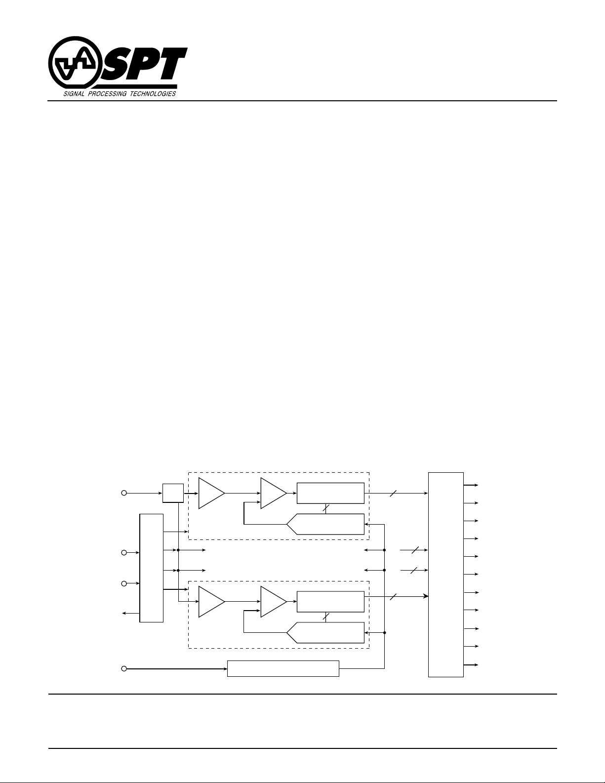
BLOCK DIAGRAM
A
CLK In
Enable
Data
Valid
Ref
ADC Section 1
Timing
and
Control
Mux
P1
P2
P7
P8
1:8
.
.
.
IN
In
T/H
ADC Section 2
ADC Section 7
ADC Section 8
T/H
.
.
.
Auto-
Zero
CMP
Auto-
Zero
CMP
Reference Ladder
11-Bit
SAR
DAC
11-Bit
SAR
DAC
11
11
11
.
.
.
11
V
REF
.
.
.
11
11
11-Bit
8:1
Mux/
Error
Correction
Signal Processing Technologies, Inc.
4755 Forge Road, Colorado Springs, Colorado 80907, USA
Phone: 719-528-2300 Fax: 719-528-2370 Web Site: http://www .spt.com e-mail: sales@spt.com
D10 Overrange
D9 (MSB)
D8
D7
D6
D5
D4
D3
D2
D1
D0 (LSB)
Page 2

ABSOLUTE MAXIMUM RATINGS (Beyond which damage may occur)1 25 °C
Supply Voltages
AVDD......................................................................+6 V
Output
Digital Outputs ...................................................10 mA
DVDD.....................................................................+6 V
Temperature
Input Voltages
Analog Input .............................. –0.5 V to AVDD +0.5 V
..............................................................0 to AV
V
REF
CLK Input ............................................................... V
AVDD – DVDD..................................................±100 mV
AGND – DGND ..............................................±100 mV
DD
DD
Operating T emper ature ............................ –40 to 85 °C
Junction Temperature ........................................ 175 °C
Lead Temperature, (soldering 10 seconds) ....... 300 °C
Storage Temperature............................ –65 to +150 °C
Note: 1. Operation at any Absolute Maximum Rating is not implied. See
Electrical Specifications for proper nominal applied conditions
in typical applications.
ELECTRICAL SPECIFICATIONS
TA=T
to T
MIN
, AVDD=DVDD=OVDD=+5.0 V , VIN=0 to 4 V, ƒ
MAX
TEST TEST SPT7850
PARAMETERS CONDITIONS LEVEL MIN TYP MAX UNITS
Resolution 10 Bits
DC Accuracy 100 kHz clock rate
Integral Linearity Error (ILE) V ±1.0 LSB
Differential Linearity Error (DLE) V ±0.5 LSB
No Missing Codes VI Guaranteed
Analog Input
Input Voltage Range VI V
Input Resistance IV 50 kΩ
Input Capacitance V 5.0 pF
Input Bandwidth (Small Signal) V 100 MHz
Offset V ±2.0 LSB
Gain Error V ±2.0 LSB
=40 MHz, ƒS=20 MSPS, V
CLK
1
RHS
RLS
=4.0 V , V
=0.0 V, unless otherwise specified.
RLS
V
RHS
V
Reference Input
Resistance VI 400 500 600 Ω
Bandwidth V 100 150 MHz
Voltage Range
IV 0 2.0 V
IV 3.0 AV
DD
V 1.0 4.0 5.0 V
V
∆(V
∆(V
V
V
V
RLS
RHS
RHS
RHF
RLS
– V
RLS
– V
)V90mV
RHS
– V
)V75mV
RLF
Reference Settling Time
V
RHS
V
RLS
V 15 Clock Cycles
V 20 Clock Cycles
Conversion Characteristics
Maximum Conversion Rate VI 20 MHz
Minimum Conversion Rate V 50 kHz
Pipeline Delay (Latency) IV 12 Clock Cycles
Aperture Delay Time V 5 ns
Aperture Jitter Time V 30 ps (p-p)
Dynamic Performance
Effective Number of Bits (ENOB)
= 3.58 MHz VI 8.8 Bits
ƒ
IN
= 10.3 MHz VI 8.5 Bits
ƒ
IN
Signal-to-Noise Ratio (SNR)
(without Harmonics)
= 3.58 MHz VI 53 56 dB
ƒ
IN
ƒIN = 10.3 MHz VI 52 55 dB
1
SPT7850SCN is screened for DC accuracy tests at 100 kHz. SPT7850SIS and SPT7850SCT are screened f or DC accuracy tests at 35 MHz.
SPT
SPT7850
2 6/15/01
Page 3

ELECTRICAL SPECIFICATIONS
TA=T
to T
MIN
, AVDD=DVDD=OVDD=+5.0 V , VIN=0 to 4 V, ƒ
MAX
TEST TEST SPT7850
PARAMETERS CONDITIONS LEVEL MIN TYP MAX UNITS
Dynamic Performance
Total Harmonic Distortion (THD)
= 3.58 MHz VI 56 59 dB
ƒ
IN
= 10.3 MHz VI 53 56 dB
ƒ
IN
Signal-to-Noise and Distortion
(SINAD)
= 3.58 MHz VI 52 55 dB
ƒ
IN
ƒ
= 10.3 MHz VI 50 53 dB
IN
Spurious Free Dynamic Range ƒ
= 1 MHz V 63 dB
IN
Digital Inputs
Logic 1 Voltage VI 2. 0 V
Logic 0 Voltage VI 0.8 V
Maximum Input Current Low VI –10 +10 µA
Maximum Input Current High VI –10 +10 µA
Input Capacitance V 5 pF
=40 MHz, ƒS=20 MSPS, V
CLK
RHS
=4.0 V , V
=0.0 V, unless otherwise specified.
RLS
Digital Outputs
Logic 1 Voltage I
Logic 0 Voltage I
t
RISE
t
FALL
Output Enable to Data Output Delay 20 pF load, T
= 0.5 mA VI 3. 5 V
OH
= 1.6 mA VI 0.4 V
OL
15 pF load V 10 ns
15 pF load V 10 ns
= +25 °CV 10 ns
A
50 pF load over temp. V 22 ns
Power Supply Requirements
Voltages OV
DV
AV
Currents AI
DI
DD
DD
DD
DD
DD
IV 3.0 5.25 V
IV 4.75 5.0 5.25 V
IV 4.75 5.0 5.25 V
VI 10 12 mA
VI 18 21 mA
Power Dissipation VI 140 165 m W
TEST LEVEL CODES
All electrical characteristics are subject to the
following conditions:
All parameters having min/max specifications
are guaranteed. The Test Level column indicates the specific device testing actually performed during production and Quality Assurance inspection. Any blank section in the data
column indicates that the specification is not
tested at the specified condition.
LEVEL TEST PROCEDURE
I 100% production tested at the specified temperature.
II 100% production tested at TA = +25 °C, and sample tested at the
specified temperatures.
III QA sample tested only at the specified temperatures.
IV Parameter is guaranteed (but not tested) by design and characteri-
zation data.
V Parameter is a typical value for information pur poses only.
VI 100% production tested at TA = +25 °C. Parameter is guaranteed
over specified temperature range.
SPT
SPT7850
3 6/15/01
Page 4

SPECIFICATION DEFINITIONS
APERTURE DELAY
Aperture delay represents the point in time, relative to the
rising edge of the CLOCK input, that the analog input is
sampled.
APERTURE JITTER
The variations in aperture delay for successive samples.
EFFECTIVE NUMBER OF BITS (ENOB)
SINAD = 6.02N + 1.76, where N is equal to the effective
number of bits.
SINAD – 1.76
N =
INPUT BANDWIDTH
Small signal (50 mV) bandwidth (3 dB) of analog input
stage.
DIFFERENTIAL LINEARITY ERROR (DLE)
Error in the width of each code from its theoretical value.
(Theoretical = VFS/2N)
INTEGRAL LINEARITY ERROR (ILE)
Linearity error refers to the deviation of each individual
code (normalized) from a straight line drawn from –FS
through +FS. The deviation is measured from the edge of
each particular code to the true straight line.
6.02
OUTPUT DELAY
Time between the clock’s triggering edge and output data
valid.
OVERVOLTAGE RECOVERY TIME
The time required for the ADC to recover to full accuracy
after an analog input signal 125% of full scale is reduced
to 50% of the full-scale value.
SIGNAL-TO-NOISE RATIO (SNR)
The ratio of the fundamental sinusoid power to the total
noise power. Harmonics are excluded.
SIGNAL-TO-NOISE AND DISTORTION (SINAD)
The ratio of the fundamental sinusoid power to the total
noise and distortion power.
TOTAL HARMONIC DISTORTION (THD)
The ratio of the total power of the first 9 harmonics to the
power of the measured sinusoidal signal.
SPURIOUS FREE DYNAMIC RANGE (SFDR)
The ratio of the fundamental sinusoidal amplitude to the
single largest harmonic or spurious signal.
SPT
SPT7850
4 6/15/01
Page 5

Figure 1A – Timing Diagram 1
1234567891011121314151617
ANALOG IN
CLOCK IN
SAMPLING CLOCK
(Internal)
DIGITAL OUT
DATA VALID
Figure 1B – Timing Diagram 2
VALIDINVALID
4
5 6 71 2 3 8 9 10 11
t
C
CLOCK
IN
t
OD
DATA
OUTPUT
Data 0
DATA
VALID
t
S
Table I – Timing Parameters
DESCRIPTION PARAMETERS MIN TYP MAX UNITS
Conversion Time t
Clock Period t
Clock High Duty Cycle t
Clock Low Duty Cycle t
Clock to Output Delay (15 pF Load) t
DAV Pulse Width t
Clock to DAV t
t
CH
t
CLK
t
CL
Data 1 Data 2
t
DAV
C
CLK
CH
CL
OD
DAV
S
2*t
t
DAV
CLK
ns
25 ns
40 50 60 %
40 50 60 %
15 20 25 ns
t
CLK
ns
16 21 26 ns
SPT
SPT7850
5 6/15/01
Page 6

TYPICAL PERFORMANCE CHARACTERISTICS
80
70
60
50
40
Signal-to-Noise Ratio (dB)
30
20
80
10
SNR vs Input Frequency
80
70
S = 20 MSPS
60
50
40
Total Harmonic Distortion (dB)
30
20
0
10
1
10
2
Input Frequency (MHz)
10
0
THD vs Input Frequency
s = 20 MSPS
1
Input Frequency (MHz)
10
10
2
Total Power Dissipation vs Sample Rate
SINAD vs Input Frequency
170
Reference is Excluded = 30 mW Typ
70
60
50
40
30
Signal-to-Noise and Distortion (dB)
20
10
S =20 MSPS
0
10
1
10
Input Frequency (MHz)
150
130
110
Power Dissipation (mW)
90
70
2
5 10 15 20
Sample Rate (CLK/2) MHz
SPT
SPT7850
6 6/15/01
Page 7

A
Figure 2 – Typical Interface Circuit
Ref In
(+4 V)
V
IN
CLK IN
+A5
AGND
V
RHF
V
RHS
V
RLS
V
RLF
SPT7850
V
IN
V
CAL
CLK
DAV
AVDDAGND DGND* DV
+A5
OGND
L1
D10
D9
D8
D7
D6
D5
OV
DD
D4
D3
D2
D1
D0
EN
DD
Enable/Tri-State
(Enable = Active Low)
3.3/5
Interfacing
Logics
DGND
3.3/5
3.3/5
+
10 µF
+5 V
nalog
+5 V
Analog
RTN
NOTES: 1) L1 is to be located as closely to the device as possible.
*To reduce the possibility of latch-up, avoid
connecting the DGND pins of the ADC to the
digital ground of the system.
2) All capacitors are 0.1 µF surface-mount unless otherwise specified.
3) L1 is a 10 µH inductor or a ferrite bead.
TYPICAL INTERFACE CIRCUIT
V ery few e xternal components are required to achiev e the
stated device performance. Figure 2 shows the typical interface requirements when using the SPT7850 in normal
circuit operation. The following sections provide descriptions of the major functions and outline critical performance criteria to consider for achieving the optimal device
performance.
POWER SUPPLIES AND GROUNDING
SPT suggests that both the digital and the analog supply
voltages on the SPT7850 be derived from a single analog
supply as shown in figure 2. A separate digital supply
should be used for all interface circuitry. SPT suggests
using this power supply configuration to prev ent a possible
latch-up condition on powerup.
+
10 µF
+5 V
Digital
RTN
+5 V
Digital
OPERATING DESCRIPTION
The general architecture for the CMOS ADC is shown in
the block diagram. The design contains eight identical
successive approximation ADC sections, all operating in
parallel, a 16-phase clock generator, an 11-bit 8:1 digital
output multiplexer, correction logic, and a voltage reference generator that provides common reference le vels f or
each ADC section.
The high sample rate is achieved by using multiple SAR
ADC sections in parallel, each of which samples the input
signal in sequence. Each ADC uses 16 clock cycles to
complete a conversion. The clock cycles are allocated as
shown in table II.
SPT
7 6/15/01
SPT7850
Page 8

Table II – Clock Cycles
Figure 3 – Ladder Force/Sense Circuit
Clock Operation
1 Reference zero sampling
2 Auto-zero comparison
3 Auto-calibrate comparison
4 Input sample
5-15 11-bit SAR conversion
16 Data transfer
The 16-phase clock, which is derived from the input clock,
synchronizes these ev ents. The timing signals f or adjacent
ADC sections are shifted by two clock cycles so that the
analog input is sampled on every other cycle of the input
clock by exactly one ADC section. After 16 clock periods,
the timing cycle repeats. The sample rate for the configuration is one-half of the clock rate; e.g., f or a 40 MHz cloc k
rate, the input sample rate is 20 MHz. The latency from
analog input sample to the corresponding digital output is
12 clock cycles.
• Since only eight comparators are used, a huge power
savings is realized.
• The auto-zero operation is done using a closed loop
system that uses multiple samples of the comparators’
response to a reference zero.
• The auto-calibrate operation, which calibrates the gain
of the MSB reference and the LSB reference, is also
done with a closed loop system. Multiple samples of the
gain error are integrated to produce a calibration voltage for each ADC section.
• Capacitive displacement currents, which can induce
sampling error, are minimiz ed since only one comparator samples the input during a clock cycle.
• The total input capacitance is very low since sections of
the converter that are not sampling the signal are isolated from the input by transmission gates.
VOLTAGE REFERENCE
The SPT7850 requires the use of a single external voltage
reference for driving the high side of the reference ladder.
It must be within the range of 3 V to 5 V. The lower side of
the ladder is typically tied to AGND (0.0 V), but can be run
up to 2.0 V with a second reference. The analog input v oltage range will track the total voltage difference measured
between the ladder sense lines, V
RHS
and V
RLS
.
Force and sense taps are provided to ensure accurate
and stable setting of the upper and lower ladder sense line
voltages across part-to-part and temperature variations.
By using the configuration shown in figure 3, offset and
gain errors of less than ±2 LSB can be obtained.
In cases where wider variations in offset and gain can be
tolerated, V
be tied directly to V
can be tied directly to V
REF
as shown in figure 4. Decouple
RLF
, and AGND can
RHF
AGND
+
+
V
RHF
V
RHS
V
RLS
V
RLF
V
IN
All capacitors are 0.01 µF
Figure 4 – Reference Ladder
+4.0 V
External
Reference
(+3.91 V)
(0.075 V)
V
RHS
V
RLS
V
RLF
(AGND)
0.0 V
90 mV
75 mV
R/2
R
R
R
R
R
R
R/2
R=30 W (typ)
All capacitors are 0.01 µF
force and sense lines to AGND with a .01 µF capacitor
(chip cap preferred) to minimize high-frequency noise injection. If this simplified configur ation is used, the following
considerations should be taken into account.
The reference ladder circuit shown in figure 4 is a simplified representation of the actual reference ladder with
force and sense taps shown. Due to the actual inter nal
structure of the ladder, the voltage drop from V
is not equivalent to the voltage drop from V
RLF
RHF
to V
to V
RLS
RHS
.
SPT
SPT7850
8 6/15/01
Page 9

Typically, the top side voltage drop for V
RHF
to V
RHS
will
equal:
V
– V
RHF
and the bottom side voltage drop for V
= 2.25 % of (V
RHS
RHF
– V
) (typical),
RLF
RLS
to V
RLF
will
equal:
V
RLS
– V
= 1.9 % of (V
RLF
RHF
– V
) (typical).
RLF
Figure 4 shows an example of expected voltage drops for
a specific case. V
is tied to AGND. A 90 mV drop is seen at V
and a 75 mV increase is seen at V
of 4.0 V is applied to V
REF
RLS
, and V
RHF
(= 3.91 V),
RHS
(= 0.075 V).
RLF
ANALOG INPUT
VIN is the analog input. The input voltage range is from
V
RLS
to V
(typically 4.0 V) and will scale proportionally
RHS
with respect to the voltage reference. (See voltage reference section.)
The drive requirements for the analog inputs are very
minimal when compared to most other converters due to
the SPT7850’s extremely low input capacitance of only
5 pF and very high input resistance of 50 kΩ.
The analog input should be protected through a series
resistor and diode clamping circuit as shown in figure 5.
Upon powerup, the SPT7850 begins its calibration algorithm. In order to achieve the calibration accuracy required, the offset and gain adjustment step size is a fraction of a 10-bit LSB. Since the calibration algorithm is an
oversampling process, a minimum of 10,000 clock cycles
are required. This results in a minimum calibration time
upon powerup of 250 µsec for a 20 MHz sample rate.
Once calibrated, the SPT7850 remains calibrated over
time and temperature.
Since the calibration cycles are initiated on the rising edge
of the clock, the clock must be continuously applied f or the
SPT7850 to remain in calibration.
INPUT PROTECTION
All I/O pads are protected with an on-chip protection
circuit shown in figure 6. This circuit provides ESD robustness to 3.5 kV and prevents latch-up under severe discharge conditions without degrading analog transition
times.
Figure 6 – On-Chip Protection Circuit
V
DD
120 W
Analog
Figure 5 – Recommended Input Protection Circuit
+V
D1
Buffer
47 W
D2
V
D1 = D2 = Hewlett-Packard HP5712 or equivalent
AV
DD
ADC
CALIBRATION
The SPT7850 uses an auto-calibration scheme to ensure
10-bit accuracy over time and temperature. Gain and offset errors are continually adjusted to 10-bit accuracy
during device operation. This process is completely transparent to the user.
120 W
Pad
POWER SUPPLY SEQUENCING CONSIDERATIONS
All logic inputs should be held low until power to the de vice
has settled to the specific tolerances. Avoid power decoupling networks with large time constants that could delay
VDD power to the device.
CLOCK INPUT
The SPT7850 is driven from a single-ended TTL-input
clock. Because the pipelined architecture operates on the
rising edge of the clock input, the device can operate o ver
a wide range of input clock duty cycles without degrading
the dynamic performance. The device’s sample rate is
1/2 of the input clock frequency. (See figure 1A timing
diagram.)
SPT
SPT7850
9 6/15/01
Page 10

DIGITAL OUTPUTS
OVERRANGE OUTPUT
The digital outputs (D0–D10) are driven by a separate
supply (OV
makes it possible to drive the SPT7850’s TTL/CMOScompatible outputs with the user’s logic system supply.
The format of the output data (D0–D9) is straight binary.
(See table III.) The outputs are latched on the rising edge
of CLK. These outputs can be switched into a tri-state
mode by bringing EN high.
Table III – Output Data Information
ANALOG INPUT OVERRANGE OUTPUT CODE
+F.S. + 1/2 LSB 1 1 1 1 1 1 1 1 1 1 1
+F.S. –1/2 LSB 0 1 1 1 1 1 1 1 1 1Ø
+1/2 F.S. 0 ØØ ØØØØ ØØØØ
+1/2 LSB 0 0 0 0 0 0 0 0 0 0 Ø
0.0 V 0 0 0 0 0 0 0 0 0 0 0
(Ø indicates the flickering bit between logic 0 and 1.)
) ranging from +3 V to +5 V. This feature
DD
D10 D9–D0
The OVERRANGE OUTPUT (D10) is an indication that
the analog input signal has exceeded the positive fullscale input voltage by 1 LSB. When this condition occurs,
D10 will switch to logic 1. All other data outputs (D0 to D9)
will remain at logic 1 as long as D10 remains at logic 1.
This feature makes it possible to include the SPT7850 in
higher resolution systems.
EVALUATION BOARD
The EB7850 evaluation board is av ailable to aid designers
in demonstrating the full performance of the SPT7850.
This board includes a reference circuit, clock driv er circuit,
output data latches, and an on-board reconstruction of the
digital data. An application note describing the operation
of this board, as well as information on the testing of the
SPT7850, is also available. Contact the factory for price
and availability.
SPT
SPT7850
10 6/15/01
Page 11

PACKAGE OUTLINES
28-Lead SOIC
B
28
1
CD
H
E
INCHES MILLIMETERS
SYMBOL MIN MAX MIN MAX
A 0.699 0.709 17.75 18.01
I
H
A
F
G
B 0.005 0.011 0.13 0.28
C 0.050 typ 1.27 typ
D 0.018 typ 0.46 typ
E 0.0077 0.0083 0.20 0.21
F 0.090 0.096 2.29 2.44
G 0.031 0.039 0.79 0.99
H 0.396 0.416 10.06 10.57
I 0.286 0.292 7.26 7.42
C D
32-Lead TQFP
A
B
E
F
K
GH
SYMBOL MIN MAX MIN MAX
A 0.346 0.362 8.80 9.20
B 0.272 0.280 6.90 7.10
C 0.346 0.362 8.80 9.20
D 0.272 0.280 6.90 7.10
E 0.031 typ 0.80 BSC
F 0.012 0.016 0.30 0.40
G 0.053 0.057 1.35 1.45
H 0.002 0.006 0.05 0.15
I 0.037 0.041 0.95 1.05
J 0.007 0.17
I
J
L
K0° 7° 0° 7°
L 0.020 0.030 0.50 0.75
INCHES MILLIMETERS
SPT
SPT7850
11 6/15/01
Page 12

PACKAGE OUTLINES
28-Lead Skinny PDIP
A
D
C
B
F
E
H
I
SYMBOL MIN NOM MAX MIN NO M MAX
A 0.280 0.288 0.295 7.112 7.315 7.493
B 1.360 1.365 1.370 34.544 34.671 34.798
C 0.130 3.302
D 0.055 0.060 0.065 1.397 1.524 1.651
E 0.100 BSC 2.540 BSC
F 0.020 0.508
G 0.120 0.130 0.135 3.048 3.302 3.429
G
H 0.300 BSC 7.620 BSC
I 0.430 10.922
INCHES MILLIMETERS
SPT
SPT7850
12 6/15/01
Page 13

PIN ASSIGNMENTS
A
A
A
1
AGND
2
V
RHF
V
3
RHS
4
N/C
5
V
RLS
V
6
RLF
V
7
IN
GND
8
V
CAL
9
AV
10
DD
DV
11
DD
DGND
12
CLK
13
14
DAV
V
V
RHS
RHF
RLS
32
30
31
V
PDIP
and
SOIC
AGND
AGND
29
28
D10
27
PIN FUNCTIONS
28
D10
27
D9
26
D8
25
D7
24
D6
23
D5
22
OV
DD
21
OGND
D4
20
D3
19
D2
18
D1
17
D0
16
15
EN
D9
D8
25
26
Name Function
AGND Analog Ground
V
V
V
V
V
V
AV
DV
RHF
RHS
RLS
RLF
CAL
IN
DD
DD
Reference High Force
Reference High Sense
Reference Low Sense
Reference Low Force
Calibration Reference
Analog Input
Analog V
Digital V
DD
DD
DGND Digital Ground
CLK Input Clock ƒ
= FS (TTL)
CLK
EN Output Enable
D0–9 Tri-State Data Output, (D0=LSB)
D10 Tri-State Output Overrange
DAV Data Valid Output
OV
DD
Digital Output Supply
OGND Digital Output Ground
N/C No Connect
V
GND
GND
V
AV
AV
DV
RLF
V
CAL
1
2
IN
3
4
5
6
DD
7
DD
8
DD
9
DV
DD
10
DGND
11
DGND
TQFP
12
CLK
16
15
14
13
D0
D1
EN
DAV
D7
24
D6
23
D5
22
OV
21
DD
OGND
20
D4
19
D3
18
D2
17
ORDERING INFORMATION
PART NUMBER TEMPERATURE RANGE PACKAGE TYPE
SPT7850SCN 0 to +70 °C 28L Plastic DIP (300 mil)
SPT7850SIS –40 to +85 °C 28L SOIC
SPT7850SCT 0 to +70 °C 32L TQFP
Signal Processing Technologies, Inc. reserves the right to change products and specifications without notice. Permission is hereby
expressly granted to copy this literature for informational purposes only. Copying this material for any other use is strictly prohibited.
WARNING – LIFE SUPPORT APPLICATIONS POLICY – SPT products should not be used within Life Support Systems without
the specific written consent of SPT. A Life Support System is a product or system intended to support or sustain life which, if it fails,
can be reasonably expected to result in significant personal injury or death.
Signal Processing Technologies believes that ultrasonic cleaning of its products may damage the wire bonding, leading to device
failure. It is therefore not recommended, and exposure of a device to such a process will void the product warranty.
SPT
SPT7850
13 6/15/01
 Loading...