

Page 1
SPT7750
8-BIT, 500 MSPS FLASH A/D CONVERTER
FEATURES
• 1:2 Demuxed ECL Compatible Outputs
• Wide Input Bandwidth - 900 MHz
• Low Input Capacitance - 15 pF (MQUAD)
• Metastable Errors Reduced to 1 LSB
• Monolithic for Low Cost
• Gray Code Output
GENERAL DESCRIPTION
The SPT7750 is a full parallel (flash) analog-to-digital converter capable of digitizing full scale (0 to -2 V) inputs into
eight-bit digital words at an update rate of 500 MSPS. The
ECL-compatible outputs are demultiplexed into two separate
output banks, each with differential data ready outputs to
ease the task of data capture. The SPT7750's wide input
bandwidth and low capacitance eliminate the need for external track-and-hold amplifiers for most applications. A propri-
CLK CLK
BLOCK DIAGRAM
CLOCK
Analog
V
RT
Input
Preamp Comparator
256
BUFFER
APPLICATIONS
• Digital Oscilloscopes
• Transient Capture
• Radar, EW, ECM
• Direct RF Down-Conversion
etary decoding scheme reduces metastable errors to the
1 LSB level. The SPT7750 operates from a single -5.2 V
supply, with a nominal power dissipation of 5.5 W.
The SPT7750 is available in an 80L surface-mount MQUAD
package over the industrial temperature range and in die
form. Contact the factory for availability of /883 versions.
DEMUX
CLOCK
BUFFER
255
152
151
128
V
RM
V
RB
127
64
63
2
1
D8
(OVR)
D7
(MSB)
D6
D5
D4
256 TO 8 BIT DECODER
D3
WITH METASTABLE ERROR CORRECTION
D2
D1
DO
(LSB)
D8B
D7B
•
•
D5B
•
•
D2B
D1B
D0B
D8A
D7A
•
•
•
1:2 DEMULTIPLEXER
D5A
•
•
•
D2A
D1A
D0A
DRB (DATA READY)
DRB (DATA READY)
D8B (OVR)
D7B (MSB)
D6B
D5B
D4B
D3B
D2B
D1B
D0B (LSB)
DRA (DATA READY)
DRA (DATA READY)
D8A (OVR)
D7A (MSB)
D6A
D5A
ECL OUTPUT BUFFERS AND LATCHES
D4A
D3A
D2A
D1A
D0A (LSB)
BANK B
BANK A
Signal Processing Technologies, Inc.
4755 Forge Road, Colorado Springs, Colorado 80907, USA
Phone: (719) 528-2300 FAX: (719) 528-2370
Page 2

ABSOLUTE MAXIMUM RATINGS (Beyond which damage may occur)1 25 °C
Supply Voltages
Negative Supply Voltage (V
Ground Voltage Differential............................. .-0.5 to +0.5 V
TO GND) ......... .-7.0 to +0.5 V
EE
Output
Digital Output Current ........................................ 0 to -28 mA
Temperature
Input Voltage
Analog Input Voltage........................................ +0.5 V to V
Reference Input Voltage .................................. +0.5 V to V
Digital Input Voltage ......................................... +0.5 V to V
Reference Current VRT to VRB.................................... 35 mA
EE
EE
EE
Operating Temperature, ambient .......................-25 to +85 °C
case ................................... +125 °C
junction...............................+150 °C
Lead Temperature, (soldering 10 seconds). ............. +300 °C
Storage Temperature ......................................-65 to +150 °C
Notes: 1. Operation at any Absolute Maximum Rating is not implied. See Electrical Specifications for proper nominal applied condi-
tions in typical applications.
ELECTRICAL SPECIFICATIONS
TJ = TC = TA = +25 °C , VEE=-5.2 V, VRB=-2.00 V, VRM=-1.0 V, VRT=0.00 V, f
TEST TEST SPT7750A SPT7750B
PARAMETERS CONDITIONS LEVEL MIN TYP MAX MIN TYP MAX UNITS
Resolution 8 8 Bits
DC Accuracy
Integral Nonlinearity f
Differential Nonlinearity f
= 100 kHz I -1.0 +1.0 -1.5 +1.5 LSB
CLK
= 100 kHz I -0.85 +0.95 -0.95 +1.5 LSB
CLK
No Missing Codes Guaranteed Guaranteed
Analog Input
Input Voltage Range I V
Input Bias Current V
=0 V I .75 2.0 .75 2.0 mA
IN
Input Resistance V 15 15 kΩ
Input Capacitance Over Full Input Range V 15 15 pF
Input Bandwidth
Small Signal V 900 900 MHz
Large Signal V 500 500 MHz
Offset Error V
Offset Error V
RT
RB
Input Slew Rate V 5 5 V/ns
Clock Synchronous
Input Currents V 2 2 µA
Reference Input
Ladder Resistance I 60 80 60 80 Ω
Reference Bandwidth V 30 30 MHz
Timing Characteristics
Maximum Sample Rate I 500 500 MHz
Aperture Jitter V 2 2 ps
Acquisition Time V 250 250 ps
CLK to Data Ready Delay IV 0.9 1.4 1.9 0.9 1.4 1.9 ns
Clock to Data Delay IV 1.25 1.75 2.25 1.25 1.75 2.25 ns
Dynamic Performance
Signal-To-Noise Ratio
(without Harmonics)
= 50 MHz I 47 45 dB
f
IN
= 250 MHz I 44 42 dB
f
IN
Total Harmonic Distortion
f
= 50 MHz I -46 -44 dBc
IN
f
= 250 MHz I -38 -36 dBc
IN
=500 MHz, Duty Cycle=50%, unless otherwise specified.
clk
RB
V
RT
V
RB
VRTV
IV -30 +30 -30 +30 mV
IV -30 +30 -30 +30 mV
SPT
SPT7750
2 3/5/97
Page 3

ELECTRICAL SPECIFICATIONS
TJ = TC = TA = +25 °C , VEE=-5.2 V, VRB=-2.00 V, VRM=-1.0 V, VRT=0.00 V, f
TEST TEST SPT7750A SPT7750B
PARAMETERS CONDITIONS LEVEL MIN TYP MAX MIN TYP MAX UNITS
Dynamic Performance
Signal-to-Noise and Distortion
= 50 MHz I 43 41 dB
f
IN
= 250 MHz I 37 35 dB
f
IN
Spurious Free Dynamic Range
f
= 50 MHz I 49 44 dB
IN
f
= 250 MHz I 41 36 dB
IN
Digital Inputs
Input High Voltage
(CLK, NCLK) I -1.1 -0.7 -1.1 -0.7 V
Input Low Voltage
(CLK, NCLK) I -1.8 -1.5 -1.8 -1.5 V
Clock Pulse Width High (t
Clock Pulse Width Low (t
Digital Outputs
Logic 1 Voltage I -1.1 -0.9 -1.1 -0.9 V
Logic 0 Voltage I -1.8 -1.5 -1.8 -1.5 V
Rise Time 20% to 80% V 450 450 ps
Fall Time 20% to 80% V 450 450 ps
Power Supply Requirements
Voltage V
Current I
Power Dissipation I 5.5 6.25 5.5 6.25 W
EE
EE
) I 1.0 0.67 1.0 0.67 ns
PWH
) I 1.0 0.67 1.0 0.67 ns
PWL
=500 MHz, Duty Cycle=50%, unless otherwise specified.
clk
IV -4.95 -5.2 -5.45 -4.95 -5.2 -5.45 V
I 1.05 1.2 1.05 1.2 A
Typical Thermal Impedance: θJC = +4 °C/W.
TEST LEVEL CODES
All electrical characteristics are subject to the
following conditions:
All parameters having min/max specifications
are guaranteed. The Test Level column indicates the specific device testing actually performed during production and Quality Assurance inspection. Any blank section in the data
column indicates that the specification is not
tested at the specified condition.
Unless otherwise noted, all tests are pulsed
tests; therefore, TJ = TC = TA.
TEST LEVEL
I
II
III
IV
V
VI
TEST PROCEDURE
100% production tested at the specified temperature.
100% production tested at TA=25 °C, and sample
tested at the specified temperatures.
QA sample tested only at the specified temperatures.
Parameter is guaranteed (but not tested) by design
and characterization data.
Parameter is a typical value for information purposes
only.
100% production tested at TA = 25 °C. Parameter is
guaranteed over specified temperature range.
SPT
SPT7750
3 3/5/97
Page 4

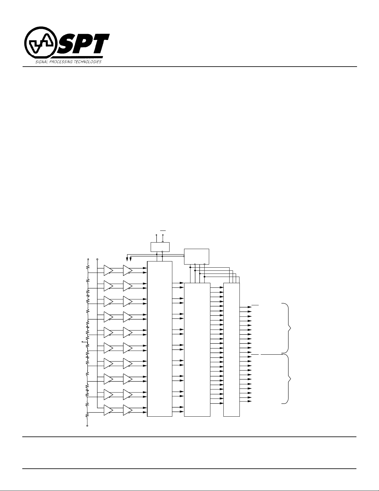
GENERAL DESCRIPTION
The SPT7750 is one of the fastest monolithic 8-bit parallel
flash A/D converters available today. The nominal conversion rate is 500 MSPS and the analog bandwidth is in excess
of 900 MHz. A major advance over previous flash converters
is the inclusion of 256 input preamplifiers between the
reference ladder and input comparators (see block diagram). This not only reduces clock transient kickback to the
input and reference ladder due to a low AC beta but also
reduces the effect of the dynamic state of the input signal on
the latching characteristics of the input comparators. The
preamplifiers act as buffers and stabilize the input capacitance so that it remains constant over different input voltage
Figure 1 - SPT7750 Typical Interface Circuit
**
V
IN
50 Ω
V
IN
V
IN
and frequency ranges and therefore makes the part easier to
drive than previous flash converters. The preamplifiers also
add a gain of two to the input signal so that each comparator
has a wider overdrive or threshold range to "trip" into or out
of the active state. This gain reduces metastable states that
can cause errors at the output.
The SPT7750 has true differential analog and digital data
paths from the preamplifiers to the output buffers (Current
Mode Logic) for reducing potential missing codes while
rejecting common mode noise.
Signature errors are also reduced by careful layout of the
analog circuitry. The output drive capability of the device can
provide full ECL swings into 50 Ω loads.
-2.0 V
Reference
Convert
V
RTF
V
*
*
50 Ω
RTS
V
RM
V
RBS
V
RBF
CLK
NCLK
-5.2 V
50 Ω
.1 µF
EE
V
AGND
DGND
FB
*
FB = Ferrite bead
U1= OP291 or equivalent with low offset/noise.
R = 1 k Ω; 0.1% matched.
= AGND
= DGND
U2= Motorola ECLinPS Lite, MC10EL16, differential receiver
with 250 ps (typ) propagation delay.
* = 10 µF Tantalum Capacitor and 0.1 µF Chip Capacitor
** = Care must be taken to avoid exceeding the maximum rating
for the input, especially during power up sequencing of the
analog input driver.
R
22 Ω
+
U1
-
R
2N2907
22 Ω
-
U1
+
-5.2 V
U2
50 Ω
-5.2 V
-2 V
Pulldown
(Analog)
DRB (DATA READY)
DRB (DATA READY)
D8B (OVR)
D7B (MSB)
D6B
D5B
D4B
D3B
D2B
D1B
D0B (LSB)
DRA (DATA READY)
DRA (DATA READY)
D8A (OVR)
D7A (MSB)
D6A
D5A
D4A
D3A
D2A
D1A
D0A (LSB)
50 Ω
-2.0 V
Pulldown
(Digital)
BANK B
BANK A
SPT
SPT7750
4 3/5/97
Page 5

V
IN
> -0.5 LSB
-0.5 LSB
-1.5 LSB
•
•
•
-1.0 V
•
•
•
-2.0 V+
1/2
LSB
< (-2.0 V +
1/2
LSB)
D8
1
1
0
0
0
•
•
•
0
0
•
•
•
0
0
0
D7 • • • D0
1 0 0 0 0 0 0 0
1 0 0 0 0 0 0 0
1 0 0 0 0 0 0 0
1 0 0 0 0 0 0 0
1 0 0 0 0 0 0 1
•
•
•
1 1 0 0 0 0 0 0
0 1 0 0 0 0 0 0
•
•
•
0 0 0 0 0 0 0 1
0 0 0 0 0 0 0 0
0 0 0 0 0 0 0 0
Indicates the transition between the two codes
TYPICAL INTERFACE CIRCUIT
The circuit in figure 1 is intended to show the most elaborate
method of achieving the least error by correcting for integral
linearity, input induced distortion and power supply/ground
noise. This is achieved by the use of external reference
ladder tap connections, input buffer and supply decoupling.
Please contact the factory for the SPT7750 evaluation board
applications note that contains more details on interfacing the
SPT7750. The function of each pin and external connections
to other components is as follows:
VEE, AGND, DGND
VEE is the supply pin with AGND as ground for the device. The
power supply pins should be bypassed as close to the device
as possible with at least a .01 µF ceramic capacitor. A 1 µF
tantalum can also be used for low frequency suppression.
DGND is the ground for the ECL outputs and is to be
referenced to the output pulldown voltage and appropriately
bypassed as shown in figure 5.
VIN (ANALOG INPUT)
There are two analog input pins that are tied to the same point
internally. Either one may be used as an analog input sense
and the other for input force. This is convenient for testing the
source signal to see if there is sufficient drive capability. The
pins can also be tied together and driven by the same source.
The SPT7750 is superior to similar devices due to a preamplifier stage before the comparators. This makes the device
easier to drive because it has constant capacitance and
induces less slew rate distortion.
(VRM) and AGND (VRT force and sense). The reference pins
and tap can be driven by op amps as shown in figure 1 or V
may be bypassed for limited temperature operation. These
voltage inputs can be bypassed to AGND for further noise
suppression if so desired.
Table I - Output Coding
RM
CLK,
The clock inputs are designed to be driven differentially with
ECL levels. The duty cycle of the clock should be kept at 50%
to avoid causing larger second harmonics. If this is not
important to the intended application, then duty cycles other
than 50% may be used.
D0 TO D8, DR, NDR, (A AND B)
(CLOCK INPUTS)
CLK
The digital outputs can drive 50 Ω to ECL levels when pulled
down to -2 V. When pulled down to -5.2 V, the outputs can
drive 130 Ω to 1 kΩ loads. All digital outputs are grey code with
the coding as shown in table 1.
V
, V
RBF
(REFERENCE INPUTS)
RBS
, V
There are two reference inputs and one external reference
voltage tap. These are -2 V (VRB force and sense), mid-tap
RTF
, V
RTS
, V
RM
SPT
THERMAL MANAGEMENT
The typical thermal impedance is as follows:
ΘCA = +17 °C/W in still air with no heat sink
We highly recommend that a heat sink be used for this device
with adequate air flow to ensure rated performance of the
device. We have found that a Thermalloy 17846 heat sink
with a minimum air flow of 1 meter/second (200 linear feet per
minute) provides adequate thermal performance under laboratory tests. Application specific conditions should be taken
into account to ensure that the device is properly heat sinked.
SPT7750
5 3/5/97
Page 6

OPERATION
The SPT7750 has 256 preamp/comparator pairs which are
each supplied with the voltage from VRT to VRB divided
equally by the resistive ladder as shown in the block diagram.
This voltage is applied to the positive input of each preamplifier/comparator pair. An analog input voltage applied at VIN is
connected to the negative inputs of each preamplifier/comparator pair. The comparators are then clocked through each
one's individual clock buffer. When the CLK pin is in the low
state, the master or input stage of the comparators compare
the analog input voltage to the respective reference voltage.
When the CLK pin changes from low to high the comparators
are latched to the state prior to the clock transition and output
logic codes in sequence from the top comparators, closest to
VRT (0 V), down to the point where the magnitude of the input
signal changes sign (thermometer code). The output of each
comparator is then registered into four 64-to-6 bit decoders
when the CLK is changed from high to low. At the output of the
decoders is a set of four 7-bit latches which are enabled
("track") when the clock changes from high to low. From here,
the output of the latches are coded into 6 LSBs from 4
columns and 4 columns are coded into 2 MSBs. Finally, 8
ECL output latches and buffers are used to drive the external
loads. The conversion takes one clock cycle from the input to
the data outputs.
Figure 2 - Timing Diagram
NCLK
DRA
NDRA
Data Bank A
DRB
NDRB
Data Bank B N-1 N+1 N+3
Figure 3 - Subcircuit Schematics
V
CLK
N
N+1
IN
2.0 ns
1.4 ns
typ
N+2
N+3
N-2 N N+2 N+4
1.75 ns
typ
1.4 ns
typ
1.75 ns
typ
N+5
N+4
N+6
V
IN
SPT
INPUT CIRCUIT OUTPUT CIRCUIT
AGND
AGND
V
R
V
EE
6 3/5/97
DGND
Data Out
CLOCK INPUT
CLK
AGND
V
CLK
EE
SPT7750
Page 7

PACKAGE OUTLINE
80-PIN MQUAD
A
B
F
C
D
E
G
H
K
L
I
J
M
INCHES MILLIMETERS
SYMBOL MIN MAX MIN MAX
A 0.937 0.945 23.80 24.00
B 0.777 0.785 19.72 19.93
C 0.472 TYP 12.0 TYP
D 0.541 0.549 13.73 13.94
E 0.701 0.709 17.80 18.00
F 0.032 TYP 0.80 TYP
G 0.014 TYP 0.36 TYP
H 0.114 0.122 2.90 3.10
I .006 TYP 0.15 TYP
J 0.724 TYP 18.4 TYP
K 0.099 0.109 2.51 2.77
L7° 7°
M 0.026 0.036 0.66 0.91
SPT
SPT7750
7 3/5/97
Page 8

PIN ASSIGNMENTS
PIN FUNCTIONS
D2B
D3B
D4B
V
EE
V
EE
D5B
DGND
D6B
DGND
D7B
DGND
D8B
N/C
N/C
AGND
AGND
AGND
AGND
V
EE
V
EE
V
RBF
V
EE
V
EE
V
RBS
10
12
13
14
15
16
17
18
19
20
21
22
23
24
V
D1B
DØB
DRB
NDRB
D8A
72
D7A
DGND
70
71
DGND
DGND
75
74
DGND
73
EE
80
78
77
76
79
1
2
3
4
5
6
7
8
9
1
1
MQUAD
25
27
29
31
33
26
28
30
32
V
AGND
AGND
EE
AGND
V
EE
V
N/C
AGND
IN
35
34
V
V
N/C
IN
RM
D6A
DGND
68
69
37
36
AGND
AGND
EE
EE
V
67
38
V
EE
D5A
66
39
V
D4A
V
EE
65
40
64
63
62
61
60
59
58
57
56
55
54
53
52
51
50
49
48
47
46
45
44
43
42
41
N/C
N/C
D3A
D2A
V
EE
D1A
DGND
DØA
DGND
NDRA
DGND
DRA
AGND
AGND
CLK
V
EE
NCLK
V
EE
V
EE
AGND
AGND
V
RTS
V
RTF
N/C
NAME FUNCTION
V
EE
Negative Supply Nominally -5.2 V
AGND Analog Ground
V
RTF
Reference Voltage Force Top,
Nominally 0 V
V
V
V
RTS
RM
RBF
Reference Voltage Sense Top
Reference Voltage Middle, Nominally -1 V
Reference Voltage Force Bottom,
Nominally -2 V
V
V
RBS
IN
Reference Voltage Sense Bottom
Analog Input Voltage, Can Be Either
Voltage or Sense
DGND Digital Ground
D0-D7A Data Output Bank A
D0-D7B Data Output Bank B
DRA Data Ready Bank A
NDRA Not Data Ready Bank A
DRB Data Ready Bank B
NDRB Not Data Ready Bank B
D8A Overrange Output Bank A
D8B Overrange Output Bank B
CLK Clock Input
NCLK Clock Input
ORDERING INFORMATION
PART NUMBER DESCRIPTION TEMPERATURE RANGE PACKAGE TYPE
SPT7750AIK INL = 1.0 LSB -25 to +85 °C 80L MQUAD
SPT7750BIK INL = 1.5 LSB -25 to +85 °C 80L MQUAD
SPT7750BCU INL = 1.5 LSB +25 °C Die*
*Please see the die specification for guaranteed electrical performance.
Signal Processing Technologies, Inc. reserves the right to change products and specifications without notice. Permission is hereby expressly
granted to copy this literature for informational purposes only. Copying this material for any other use is strictly prohibited.
WARNING - LIFE SUPPORT APPLICATIONS POLICY - SPT products should not be used within Life Support Systems without the specific
written consent of SPT. A Life Support System is a product or system intended to support or sustain life which, if it fails, can be reasonably
expected to result in significant personal injury or death.
Signal Processing Technologies believes that ultrasonic cleaning of its products may damage the wire bonding, leading to device
failure. It is therefore not recommended, and exposure of a device to such a process will void the product warranty.
SPT7750
SPT
8 3/5/97
 Loading...