

Page 1
SPT774
FAST, COMPLETE 12-BIT µP COMPATIBLE
A/D CONVERTER WITH SAMPLE/HOLD
FEATURES
• Improved Higher Performance Version of the HADC574Z
• Complete 12-Bit A/D Converter with Sample/Hold,
Reference and Clock
• Low Power Dissipation (120 mW Max)
• 12-Bit Linearity (Over Temp)
•8 µs Max Conversion Time
• Single +5 V Supply
• Full Bipolar and Unipolar Input Range
GENERAL DESCRIPTION
The SPT774 is a complete, 12-bit successive approximation
A/D converter manufactured in CMOS technology. The device is an improved version of the HADC574Z. Included on
chip are an internal reference, clock, and a sample-and-hold.
The S/H is an additional feature not available on similar
devices.
The SPT774 features 8 µs (max) conversion time of 10 or
20 V input signals. Also, a three-state output buffer is added
for direct interface to an 8-, 12- or 16-bit µP bus.
APPLICATIONS
• Data Acquisition Systems
• 8 or 12-Bit µP Input Functions
• Process Control Systems
• Test and Scientific Instruments
• Personal Computer Interface
The SPT774 has standard bipolar and unipolar input ranges
of 10 V and 20 V that are controlled by a bipolar offset pin and
laser trimmed for specified linearity, gain and offset accuracy.
The power supply is +5 V. The device also has an optional
mode control voltage which may be used depending on the
application. With a maximum dissipation of 120 mW at the
specified voltages, power consumption is about five times
lower than that of currently available devices.
The SPT774 is available in 28-lead ceramic sidebrazed DIP,
PDIP and SOIC packages in the commercial temperature
range.
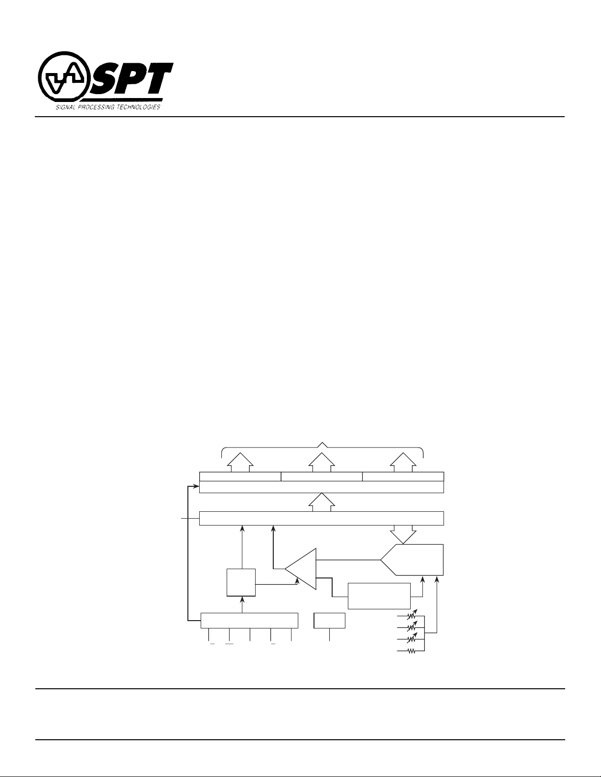
BLOCK DIAGRAM
Signal Processing Technologies, Inc.
Phone: (719) 528-2300 FAX: (719) 528-2370 Website: http://www.spt.com E-Mail: sales@spt.com
Output
Nibble A Nibble B Nibble C
Three-State Buffers And Control
STS
Clock
Control Logic
A
12/8 CS R/C
oCE
12-Bit SAR
Comp
+
-
Ref Out
Ref
Capacitance
Offset/Gain
Trim
20 V In
10 V In
BIP Off
AGND
4755 Forge Road, Colorado Springs, Colorado 80907, USA
12-Bit
DAC
Page 2
ABSOLUTE MAXIMUM RATINGS (Beyond which damage may occur) 1 25 °C
Supply Voltages
Mode Control Voltage (VEE to DGND) ....................0 to +7 V
Logic Supply Voltage (VDD to DGND) ...................0 to +7 V
Analog to Digital Ground (AGND to DGND) .................±1 V
Input Voltages
Control Input Voltages (to DGND)
(CE, CS, Ao, 12/8, R/C)......................... -0.5 to VDD +0.5 V
Analog Input Voltage (to AGND)
(REF IN, BIP OFF, 10 VIN) ......................................±16.5 V
20 V VIN Input Voltage (to AGND) ..............................±24 V
Note: Operation at any Absolute Maximum Rating is not implied. See Operating Conditions for proper nominal applied
conditions in typical applications.
Output
Reference Output Voltage ..............Indefinite Short to GND
Momentary Short to V
Temperature
Operating Temperature, Ambient .................... 0 to +70 °C
Junction.........................+165 °C
Lead Temperature, (Soldering 10 Seconds)...........+300 °C
Storage Temperature....................................-65 to +150 °C
ELECTRICAL SPECIFICATIONS
DD
TA = T
PARAMETER CONDITIONS LEVEL MIN TYP MAX MIN TYP MAX UNITS
MIN
to T
MAX
, V
EE
= 0 to +5 V, V
TEST TEST SPT774C SPT774B
= +5 V, fS = 117 kHz, fIN = 10 kHz, unless otherwise specified..
DD
DC ELECTRICAL CHARACTERISTICS
Resolution VI 12 12 Bits
Linearity Error TA= 0 to +70 °CVI ±1 ±0.5 LSB
Differential Linearity No Missing Codes VI 12 12 Bits
Unipolar Offset; 10 V, 20 V +25 °C Adjustable to Zero VI ±2 ±2 LSB
Bipolar Offset; ±5 V, ±10 V +25 °C Adjustable to Zero VI ±10 ±4 LSB
Full Scale Calibration Error
Full Scale Calibration Error1No Adjustment to Zero
Temperature Coefficients Using Internal Reference
Unipolar Offset V ±1.0 ±1.0 ppm/°C
Bipolar Offset V ±2.0 ±2.0 ppm/°C
Full Scale Calibration V ±12 ±12 ppm/°C
Power Supply Rejection Max change in full VI ±0.5 ±0.5 LSB
+4.75 V<VDD<+5.25 V scale calibration
Analog Input Ranges
Bipolar VI -5 +5 -5 +5 Volts
Unipolar VI 0 +10 0 +10 Volts
Input Impedance
10 Volt Span VI 8.5 12 8.5 12 kΩ
20 Volt Span VI 35 50 35 50 kΩ
1
+25 °C Adjustable to Zero VI 0.30 0.30 % of FS
TA = 0 to +70 °C V 0.47 0.37 % of FS
VI -10 +10 -10 +10 Volts
VI 0 +20 0 +20 Volts
SPT
SPT774
2 8/1/00
Page 3
ELECTRICAL SPECIFICATIONS
TA = T
MIN
to T
MAX
, V
EE
= 0 to +5 V, V
= +5 V, fS = 117 kHz, fIN = 10 kHz, unless otherwise specified.
DD
TEST TEST SPT774C SPT774B
PARAMETER CONDITIONS LEVEL MIN TYP MAX MIN TYP MAX UNITS
DC ELECTRICAL CHARACTERISTICS
Power Supplies Operating
Voltage Range
V
DD
2
V
EE
Operating Current
I
DD
IEE2V
= +5 V IV 167 167 µA
EE
Power Dissipation VI 75 120 75 120 mW
Internal Reference
Voltage VI 2.4 2.5 2.6 2.4 2.5 2.6 Volts
Output Current
3
DIGITAL CHARACTERISTICS
Logic Inputs
(CE,
, R/C, Ao, 12/8)
CS
Logic 0 VI -0.5 +0.8 -0.5 +0.8 Volts
Logic1 VI 2.0 5.5 2.0 5.5 Volts
Current VI -5.0 0. 1 5.0 -5.0 0. 1 5.0 µA
Capacitance V 5 5 pF
Logic Outputs
(DB11-DB0, STS)
Logic 0 (I
Logic 1 (I
= 1.6 mA) VI +0.4 +0.4 Volts
Sink
SOURCE
= 500 µA) VI +2.4 +2.4 Volts
Leakage (High Z State, VI -5 0.1 +5 -5 0.1 +5 µA
DB11-DB0 Only)
Capacitance V 5 5 pF
AC Accuracy fS=117 kHz, fIN=10 kHz
Spurious Free Dyn. Range V 73 78 76 78 dB
Total Harmonic Distortion V -77 -72 -77 -75 dB
Signal-to-Noise Ratio V 69 72 71 72 dB
Signal-to-Noise & Distortion V 68 71 70 71 dB
(SINAD)
Intermodulation Distortion fIN=20 kHz; V -75 -75 dB
f
=23 kHz
IN2
Note 1: Fixed 50 Ω resistor from REF OUT to REF IN and REF OUT to BIP OFF.
Note 2: VEE is optional and is only used to set the mode for the internal sample/hold. When not using VEE, the pin should be treated
as a no connect. If V
is connected to 0 to -15 V, aperture delay (tAP) will increase from 20 ns (typ) to 4000 ns (typ).
EE
Note 3: Available for external loads; external load should not change during conversion.
IV +4.5 +5.5 +4.5 +5.5 Volts
IV V
DD
V
DD
Volts
IV 15 24 15 24 mA
VI 0.5 0.5 mA
SPT
SPT774
3 8/1/00
Page 4
ELECTRICAL SPECIFICATIONS
TA = T
MIN
to T
MAX
, V
EE
= 0 to +5 V, V
= +5 V, fS = 117 kHz, fIN = 10 kHz, unless otherwise specified.
DD
TEST TEST SPT774C SPT774B
PARAMETER CONDITIONS LEVEL MIN TYP MAX MIN TYP MAX UNITS
AC ELECTRICAL CHARACTERISTICS
4
Convert Mode Timing
t
STS Delay from CE VI 60 200 60 200 ns
DSC
t
CE Pulse Width VI 50 30 50 30 ns
HEC
t
CS to CE Setup VI 50 20 50 20 ns
SSC
CS Low during CE High VI 50 20 50 20 ns
t
HSC
R/C to CE Setup VI 50 0 50 0 ns
t
SRC
R/C Low During CE High VI 50 20 50 20 ns
t
HRC
t
Ao to CE Setup VI 0 0 ns
SAC
Ao Valid During CE High VI 50 20 50 20 ns
t
HAC
t
Conversion Time
C
5
12-Bit Cycle VI 7.5 8 7.5 8 µs
8-Bit Cycle VI 5.5 5.9 5.5 5.9 µs
Read Mode Timing
Access Time from CE VI 75 150 75 150 ns
t
DD
t
Data Valid After CE Low VI 25 35 25 35 ns
HD
t
Output Float Delay VI 100 150 100 150 ns
HL
CS to CE Setup VI 50 0 50 0 ns
t
SSR
R/C to CE Setup VI 0 0 ns
t
SRR
t
Ao to CE Setup VI 50 25 50 25 ns
SAR
CS Valid After CE Low VI 0 0 ns
t
HSR
R/C High After CE Low VI 0 0 ns
t
HRR
t
STS Delay After Data Valid VI 75 150 375 75 150 375 ns
HS
t
Ao Valid after CE Low VI 50 50 ns
HAR
Note 4: Time is measured from 50% level of digital transitions.
Note 5: Includes acquisition time.
Figure 1 - Convert Mode Timing Diagram Figure 2 - Read Mode Timing Diagram
CE
CE
CS
R/C
Ao
STS
DB11-DB0
SPT
t
t
t
SSC
SRC
SAC
t
t
t
t
DSC
High Impedance
HSC
HRC
HAC
t
HEC
t
C
4 8/1/00
R/C
STS
DB11-DB0
CS
Ao
t
SSR
t
SRR
t
SAR
HIGH
IMPEDANCE
t
DD
t
HSR
t
HRR
t
HAR
t
HS
DATA
VALID
t
HL
t
HD
SPT774
Page 5

ELECTRICAL SPECIFICATIONS
TA = T
MIN
to T
MAX
, V
EE
= 0 to +5 V, V
= +5 V, fS = 117 kHz, fIN = 10 kHz, unless otherwise specified.
DD
TEST TEST SPT774C SPT774B
PARAMETER CONDITIONS LEVEL MIN TYP MAX MIN TYP MAX UNITS
AC ELECTRICAL CHARACTERISTICS
4
Stand-Alone Mode Timing
Low R/C Pulse Width VI 25 25 ns
t
HRL
STS Delay from R/
t
DS
Data Valid After R/C Low VI 25 25 ns
t
HDR
t
STS Delay After Data Valid VI 75 150 375 75 150 375 ns
HS
t
High R/C Pulse Width VI 100 100 ns
HRH
t
Data Access Time VI 150 150 ns
DDR
C
VI 200 200 ns
Sample-and-Hold
Aperture Delay VEE = +5 V IV 20 20 ns
Aperture Uncertainty Time VEE = +5 V V 300 300 ps, RMS
TEST LEVEL CODES
All electrical characteristics are subject to the
following conditions:
All parameters having min/max specifications
are guaranteed. The Test Level column indicates the specific device testing actually performed during production and Quality Assurance inspection. Any blank section in the data
column indicates that the specification is not
tested at the specified condition.
TEST LEVEL
I
II
III
IV
V
VI
TEST PROCEDURE
100% production tested at the specified temperature.
100% production tested at TA=25 °C, and sample
tested at the specified temperatures.
QA sample tested only at the specified temperatures.
Parameter is guaranteed (but not tested) by design
and characterization data.
Parameter is a typical value for information purposes
only.
100% production tested at TA = 25 °C. Parameter is
guaranteed over specified temperature range.
Figure 3 - Low Pulse for R/C - Outputs Enabled
After Conversion
t
HRL
R/C
t
DS
STS
t
HDR
t
C
t
HS
DATA VALIDDATA VALIDDB11-DB0
SPT
Figure 4 - High Pulse for R/C - Outputs Enabled While
R/C is High, Otherwise High Impedance
R/C
STS
DB11-DB0
HIGH-Z
t
t
DDR
HRH
t
HDR
DATA VALID
t
DS
t
C
HIGH-Z
SPT774
5 8/1/00
Page 6

CIRCUIT OPERATION
The SPT774 is a complete 12-bit analog-to-digital converter
that consists of a single chip version of the industry standard
774. This single chip contains a precision 12-bit capacitor
digital-to-analog converter (CDAC) with voltage reference,
comparator, successive approximation register (SAR), sampleand-hold, clock, output buffers and control circuitry to make it
possible to use the SPT774 with few external components.
other 774 circuits will cause a transient load current on the
sample-and-hold which will upset the buffer output and may
add error to the conversion itself.
Furthermore, the isolation of the input after the acquisition
time in the SPT774 allows the user an opportunity to release
the hold on an external sample-and-hold and start it tracking
the next sample. This increases system throughput with the
user’s existing components.
When the control section of the SPT774 initiates a conversion
command, the clock is enabled and the successive-approximation register is reset to all zeros. Once the conversion
cycle begins, it cannot be stopped or restarted and data is not
available from the output buffers.
The SAR, timed by the clock, sequences through the conversion cycle and returns an end-of-convert flag to the control
section of the ADC. The clock is then disabled by the control
section, the output status goes low, and the control section is
enabled to allow the data to be read by external command.
The internal SPT774 12-bit CDAC is sequenced by the SAR
starting from the MSB to the LSB at the beginning of the
conversion cycle to provide an output voltage from the CDAC
that is equal to the input signal voltage (which is divided by the
input voltage divider network). The comparator determines
whether the addition of each successively-weighted bit voltage causes the CDAC output voltage summation to be
greater or less than the input voltage; if the sum is less, the
bit is left on; if more, the bit is turned off. After testing all the
bits, the SAR contains a 12-bit binary code which accurately
represents the input signal to within ±1/2 LSB.
The internal reference provides the voltage reference to the
CDAC with excellent stability over temperature and time. The
reference is trimmed to 2.5 volts and can supply at least
0.5 mA to an external load. Any external load on the SPT774
reference must remain constant during conversion.
The sample-and-hold feature is a bonus of the CDAC architecture. Therefore the majority of the S/H specifications are
included within the A/D specifications.
Although the sample-and-hold circuit is not implemented in
the classical sense, the sampling nature of the capacitive
DAC makes the SPT774 appear to have a built-in sampleand-hold. This sample-and-hold action substantially increases the signal bandwidth of the SPT774 over that of
similar competing devices.
Note that even though the user may use an external sampleand-hold for very high frequency inputs, the internal sampleand-hold still provides a very useful isolation function. Once
the internal sample is taken by the CDAC capacitance, the
input of the SPT774 is disconnected from the user’s sampleand-hold. This prevents transients occurring during conversion from affecting the attached sample-and-hold buffer. All
TYPICAL INTERFACE CIRCUIT
The SPT774 is a complete A/D converter that is fully operational when powered up and issued a Start Convert Signal.
Only a few external components are necessary as shown in
figures 5 and 6. The two typical interface circuits are for
operating the SPT774 in either an unipolar or bipolar input
mode. Information on these connections and on conditions
concerning board layout to achieve the best operation are
discussed below.
For each application of this device, strict attention must be
given to power supply decoupling, board layout (to reduce
pickup between analog and digital sections), and grounding.
Digital timing, calibration and the analog signal source must
be considered for correct operation.
POWER SUPPLIES
The supply voltage for the SPT774 must be kept as quiet as
possible from noise pickup and also regulated from transients
or drops. Because the part has 12-bit accuracy, voltage
spikes on the supply lines can cause several LSB deviations
on the output. Switching power supply noise can be a
problem. Careful filtering and shielding should be employed
to prevent the noise from being picked up by the converter.
VDD should be bypassed with a 10 µF tantalum capacitor
located close to the converter to filter noise and counter the
problems caused by the variations in supply current. VEE is
only used as a logic input and is immune to typical supply
variation.
GROUNDING CONSIDERATIONS
Resistance of any path between the analog and digital
grounds should be as low as possible to accommodate the
ground currents present with this device.
To achieve specified accuracy, a double-sided printed circuit
board with a copper ground plane on the component side is
recommended. Keep analog signal traces away from digital
lines. It is best to lay the PC board out such that there is an
analog section and a digital section with a single point ground
connection between the two through an RF bead located as
close to the device as possible. If possible, run analog signals
between ground traces and cross digital lines at right angles
only.
SPT
SPT774
6 8/1/00
Page 7

The analog and digital common pins should be tied together
as close to the package as possible to guarantee best
performance. The code dependent currents flow through the
VDD terminal and not through the analog and digital common
pins.
RANGE CONSIDERATIONS
The SPT774 may be operated by a microprocessor or in the
stand-alone mode. The part has four standard input ranges:
0 V to +10 V, 0 V to +20 V, ±5 V and ±10 V. The maximum
errors that are listed in the specifications for gain and offset
may be adjusted externally to zero as explained in the next
two sections.
CALIBRATION & CONNECTION PROCEDURES
UNIPOLAR
The calibration procedure consists of adjusting the
converter’s most negative output to its ideal value for offset
adjustment and then adjusting the most positive output to its
ideal value for gain adjustment.
Starting with offset adjustment and referring to figure 5, the
midpoint of the first LSB increment should be positioned at
the origin to get an output code of all 0s. To do this, an input
of +1/2 LSB or +1.22 mV for the 10 V range and +2.44 mV for
the 20 V range should be applied to the SPT774. Adjust the
offset potentiometer R1 for code transition flickers between
0000 0000 0000 and 0000 0000 0001.
The gain adjustment should be done at positive full scale. The
ideal input corresponding to the last code change is applied.
This is 1 and 1/2 LSB below the nominal full scale which is
+9.9963 V for the 10 V range and +19.9927 V for the 20 V
range. Adjust the gain potentiometer R2 for flicker between
codes 1111 1111 1110 and 1111 1111 1111. If calibration is
not necessary for the intended application, replace R2 with a
50 Ω, 1% metal film resistor and remove the network from the
BIP OFF pin. Connect the BIP OFF pin to AGND. Connect the
analog input to the 10 V IN pin for the 0 to 10 V range or to the
20 V IN pin for the 0 to 20 V range.
BIPOLAR
The gain and offset errors listed in the specification may be
adjusted to zero using the potentiometers R1 and R2. (See
figure 6.) If adjustment is not needed, either or both pots may
be replaced by a 50 Ω, 1% metal film resistor.
To calibrate, connect the analog input signal to the 10 V IN pin
for a ±5 V range or to the 20 V IN pin for a ±10 V range. First
apply a DC input voltage 1/2 LSB above negative full scale
which is -4.9988 V for the ±5 V range or -9.9976 V for the ±10
V range. Adjust the offset potentiometer R1 for flicker between output codes 0000 0000 0000 and 0000 0000 0001.
Next, apply a DC input voltage 1 and 1/2 LSB below positive
full scale which is +4.9963 V for the ±5 V range or +9.9927 V
for the ±10 V range. Adjust the gain potentiometer R2 for
flicker between codes 1111 1111 1110 and 1111 1111 1111.
Figure 5 - Unipolar Input Connections
Output Bits
R/C
R1
100 kΩ
-15 V +15 V
0 to 10 V
Analog
100 kΩ
Inputs
0 to 20 V
100 Ω
R2
100 Ω
(Calibration)
V
12/8
10 V In
20 V In
BIP Off
Ref
V
CS
Ao
CE
Out
In
Ref
Control
Oscillator
Logic
Sample/Hold
MSB
Ref
Amp
V
EE
Nibble A Nibble B
Three-State Buffers And Control
12-Bits
12-Bit SAR
12-Bits
CDAC
Ref
Offset/Gain
Trim Network
Strobe
LSB
Nibble C
Comp
STS
V
DD
DGND
.1 µF
Figure 6 - Bipolar Input Connections
R/C
CS
Ao
12/8
CE
+5 V
Analog
Inputs
±5 V
±10 V
100 Ω
100 Ω
10 V In
20 V In
BIP Off
R1
V
Out
Ref
R1
V
Ref
Control
Logic
Oscillator
Sample/Hold
MSB
Ref
Amp
In
V
EE
Output Bits
Nibble A Nibble B
Three-State Buffers And Control
12-Bits
12-Bit SAR
CDAC
Strobe
LSB
Offset/Gain
Trim Network
12-Bits
Ref
Nibble C
Comp
STS
V
DD
.1 µF
DGND
+5 V
SPT
SPT774
7 8/1/00
Page 8

ALTERNATIVE
In some applications, a full scale of 10.24 V (for an LSB of
2.5 mV) or 20.48 V (for an LSB of 5.0 mV) is more convenient.
In the unipolar mode of operation, replace R2 with a 200 Ω
potentiometer and add 150 Ω in series with the 10 V IN pin for
10.24 V input range or 500 Ω in series with the 20 V IN pin for
20.48 V input range. In bipolar mode of operation, replace R1
with a 500 Ω potentiometer (in addition to the previous
changes). The calibration will remain similar to the standard
calibration procedure.
CONTROLLING THE SPT774
The SPT774 can be operated by most microprocessor systems due to the control input pins and on-chip logic. It may
also be operated in the stand-alone mode and enabled by the
R/C input pin. Full µP control consists of selecting an 8 or
12-bit conversion cycle, initiating the conversion, and reading
the output data when ready. The output read has the options
of choosing either 12-bits at once or 8 bits followed by
4-bits in a left-justified format. All five control inputs are TTL/
CMOS compatible and include 12/8, CS, Ao, R/C and CE.
The use of these inputs in controlling the converter’s operations is shown in table I, and the internal control logic is shown
in a simplified schematic in figure 10.
STAND-ALONE OPERATION
The simplest interface is a control line connected to R/C. The
output controls must be tied to known states as follows: CE
and 12/8 are wired high, Ao and CS are wired low. The output
data arrives in words of 12-bits each. The limits on R/C duty
cycle are shown in figures 3 and 4. It may have a duty cycle
within and including the extremes shown in the specifica-
tions. In general, data may be read when R/C is high unless
STS is also high, indicating a conversion is in progress.
Table I - Truth Table for the SPT774 Control Inputs
CE Ao
CS R/C 12/8
0XXXXNone
X 1 X X X None
0 0 X 0 Initiate 12 bit conversion
0 0 X 1 Initiate 8 bit conversion
1 0 X 0 Initiate 12 bit conversion
1 0 X 1 Initiate 8 bit conversion
1 0 X 0 Initiate 12 bit conversion
1 0 X 1 Initiate 8 bit conversion
10 1X1 Enable 12 bit Output
10 001 Enable 8 MSB's Only
10 011 Enable 4 LSB's Plus 4
Operation
Trailing Zeroes
Figure 7 - Interfacing the SPT774 to an 8-Bit Data Bus
Address Bus
Ao
~
STS
12/8
Ao
MSB
LSB
DIG
COM
Data
Bus
CONTROLLED OPERATION
CONVERSION LENGTH
A conversion start transition latches the state of Ao as shown
in figure 7 and table I. The latched state determines if the
conversion stops with 8 bits (Ao high) or continues for 12 bits
(Ao low). If all 12 bits are read following an 8-bit conversion, the
three LSBs will be a logic 0 and DB3 will be a logic 1. Ao is latched
because it is also involved in enabling the output buffers as
will be explained later. No other control inputs are latched.
CONVERSION START
A conversion may be initiated by a logic transition on any of
the three inputs: CE, CS, R/C, as shown in table I. The last
of the three to reach the correct state starts the conversions,
so one, two or all three may be dynamically controlled. The
nominal delay from each is the same and all three may
change state simultaneously. In order to assure that a particular input controls the start of conversion, the other two
should be set up at least 50 ns earlier. Refer to the convert
mode timing specifications. The Convert Start timing diagram
is illustrated in figure 1.
The output signal STS is the status flag and goes high only
when a conversion is in progress. While STS is high, the
output buffers remain in a high impedance state so that data
can not be read. Also, when STS is high, an additional Start
Convert will not reset the converter or reinitiate a conversion.
Note, if Ao changes state after a conversion begins, an
additional Start Convert command will latch the new start of
Ao and possibly cause a wrong cycle length for that conversion (8 versus 12 bits).
SPT
SPT774
8 8/1/00
Page 9

READING THE OUTPUT DATA
SAMPLE-AND-HOLD (S/H) CONTROL MODE
The output data buffers remain in a high impedance state until
the following four conditions are met: R/C is high, STS is low,
CE is high, and CS is low. The data lines become active in
response to the four conditions and output data according to
the conditions of 12/8 and Ao. The timing diagram for this
process is shown in figure 2. When 12/8 is high, all 12 data
outputs become active simultaneously and the Ao input is
ignored. This is for easy interface to a 12 or 16-bit data bus.
The 12/8 input is usually tied high or low, although it is
TTL/CMOS compatible. When 12/8 is low, the output is
separated into two 8-bit bytes as shown below.
Figure 8 - Output When 12/8 Is Low
BYTE 1
X X X XX X X X
MSB
This configuration makes it easy to connect to an 8-bit data
bus as shown in figure 7. The Ao control can be connected to
the least significant bit of the address bus in order to store the
output data into two consecutive memory locations. When Ao
is pulled low, the 8 MSBs are enabled only. When Ao is high,
the 4 MSBs are disabled, bits 4 through 7 are forced to a zero
and the four LSBs are enabled. The two byte format is left
justified data as shown above and can be considered to have
a decimal point or binary to the left of byte 1.
Ao may be toggled without damage to the converter at any
time. Break-before-make action is guaranteed between the
two data bytes. This assures that the outputs in figure 7 will
never be enabled at the same time.
In figure 2, it can be seen that a read operation usually begins
after the conversion is completed and STS is low. If earlier
access is needed, the read can begin no later than the
addition of time tDD and tHS before STS goes low.
BYTE 2
O O O OX X X X
LSB
This control mode is provided to allow full use of the internal
S/H, eliminating the need for an external S/H in most applications. The SPT774 in the control mode also eliminates the
need for one of the control signals, usually the convert
command. The command that puts the internal S/H in the
hold state also initiates a conversion, reducing time constraints in many systems. As soon as the conversion is
completed the internal S/H immediately begins slewing to
track the input signal. See figure 9.
In the control mode it is assumed that during the required 1.4
µs acquisition time the signal is not slewing faster than the
slew rate of the SPT774. No assumption is made about the
input level after the convert command arrives since the input
signal is sampled and conversion begins immediately after
the convert command. This means that the convert command can be used to switch an input multiplexer or change
gains on a programmable gain amplifier, allowing the input
signal to settle before the next acquisition at the end of the
conversion. Because aperture jitter is minimized by the
internal S/H, a high input frequency can be converted without
an external S/H. See table II.
Table II - Conversion Timing (VEE = +5 V)
S/H Control Mode
Parameter Min Typ Max Units
Throughput Time (tAQ+tC)
12-Bit Conversions 8 8.5 µs
8-Bit Conversions 6 6.3 µs
Conversion Time (tC)
12-Bit Conversions 6.4 µs
8-Bit Conversions 4.4 µs
Acquisition Time(tAC) 1.4 µs
Aperture Delay (tAP)20ns
Aperture Uncertainty (tJ) 0.3 ns
Figure 9 - S/H Control Mode Timing (VEE = +5 V)
R/C
t
AP
Signal Acquisition Conversion Signal Acquisition
t
AQ
SPT
t
C
SPT774
9 8/1/00
Page 10

Figure 10 - Control Logic
Input Buffers
12/8
Nibble B Zero
Override
Nibble A,B
Nibble C
CS
R/C
CE
Read Control
A
D
H
Q
CK
R
EOC8
CK
D
Q
AO Latch
Q
EOC12
Delay
STS
PACKAGE OUTLINES
28-Lead PDIP
28
1
A
B
C
SPT
J
INCHES MILLIMETERS
SYMBOL MIN MAX MIN MAX
A 0.250 6.35
B 0.115 0.200 2.92 5.08
C 0.014 0.022 0.36 0.56
K
D 0.100 2.54
E 0.030 0.070 0.76 1.78
F 0.008 0.015 0.20 0.38
G 0.125 0.195 3.18 4.95
I
H 0.600 0.625 15.24 15.88
I 0.485 0.580 12.32 14.73
J 1.380 1.565 35.05 39.75
K 0.005 0.040 0.13 1.02
H
G
F
D
E
SPT774
10 8/1/00
Page 11

PACKAGE OUTLINES
28-Lead Sidebrazed
28
1
G
A
E
B
C
D
H
SYMBOL MIN MAX MIN MAX
I
J
F
INCHES MILLIMETERS
A 0.077 0.093 1.96 2.36
B 0.016 0.020 0.41 0.51
C 0.095 0.105 2.41 2.67
D .050 typ 1.27 typ
E 0.040 0.060 1.02 1.52
F 0.215 0.235 5.46 5.97
G 1.388 1.412 35.26 35.86
H 0.585 0.605 14.86 15.37
I 0.009 0.012 0.23 0.30
J 0.600 0.620 15.24 15.75
28-Lead SOIC
B
28
1
CD
INCHES MILLIMETERS
SYMBOL MIN MAX MIN MAX
A 0.696 0.712 17.68 18.08
B 0.004 0.012 0.10 0.30
C .050 typ 1.27 typ
I H
A
F
E
H
D 0.014 0.019 0.36 0.48
E 0.009 0.012 0.23 0.30
F 0.080 0.104 2.03 2.64
G 0.016 0.050 0.41 1.27
H 0.394 0.419 10.01 10.64
I 0.291 0.299 7.39 7.59
G
SPT
SPT774
11 8/1/00
Page 12

PIN ASSIGNMENTS PIN FUNCTIONS
1
2
3
4
5
6
7
8
9
10
11
12
13
14
V
DD
12/8
CS
Ao
R/C
CE
N/C
REF OUT
AGND
REF IN
V
EE
BIP OFF
10 V IN
20 V IN
28-LEAD DIP/SOIC
STS
DB11
DB10
DB9
DB8
DB7
DB6
DB5
DB4
DB3
DB2
DB1
DB0
DGND
28
27
26
25
24
23
22
21
20
19
18
17
16
15
V
DD
12/
8
CS
Ao Byte Address/Short Cycle
R/
C
CE Chip Enable
V
EE
REF OUT Reference Output, Nominally +2.5 V
AGND Analog Ground
REF IN Reference Input
N/C Pin Not Connected to Device
BIP OFF Bipolar Offset
10 V IN 10 Volt Analog Input
Logic Supply Voltage, Nominally +5 V
Data Mode Selection
Chip Selection
Read/Convert
Mode Control Voltage, Nominally +5 V
20 V IN 20 Volt Analog Input
DGND Digital Ground
NAME FUNCTION
DB0 - DB11 Digital Data Output
DB11 - MSB DB0 - LSB
STS Status
ORDERING INFORMATION
LINEARITY ERROR PACKAGE
PART NUMBER TEMPERATURE RANGE MAX TYPE
SPT774BCN 0 to +70 °C ±1/2 LSB 28L Plastic DIP
SPT774BCJ 0 to +70 °C ±1/2 LSB 28L Sidebrazed DIP
SPT774BCS 0 to +70 °C ±1/2 LSB 28L SOIC
SPT774CCN 0 to +70 °C ±1 LSB 28L Plastic DIP
SPT774CCJ 0 to +70 °C ±1 LSB 28L Sidebrazed DIP
SPT774CCS 0 to +70 °C ±1 LSB 28L SOIC
Signal Processing Technologies, Inc. reserves the right to change products and specifications without notice. Permission is hereby expressly
granted to copy this literature for informational purposes only. Copying this material for any other use is strictly prohibited.
WARNING - LIFE SUPPORT APPLICATIONS POLICY - SPT products should not be used within Life Support Systems without the specific
written consent of SPT. A Life Support System is a product or system intended to support or sustain life which, if it fails, can be reasonably
expected to result in significant personal injury or death.
Signal Processing Technologies believes that ultrasonic cleaning of its products may damage the wire bonding, leading to device
failure. It is therefore not recommended, and exposure of a device to such a process will void the product warranty.
SPT774
SPT
12 8/1/00
 Loading...