

Page 1
SPT7734
8-BIT, 40 MSPS,175 mW A/D CONVERTER
FEATURES
• Monolithic 40 MSPS Converter
• 175 mW Power Dissipation
• On-Chip Track-and-Hold
• Single +5 V Power Supply
• TTL/CMOS Outputs
• 5 pF Input Capacitance
• Low Cost
• Tri-State Output Buffers
• High ESD Protection: 3,500 V Minimum
• Selectable +3 V or +5 V Logic I/O
GENERAL DESCRIPTION
The SPT7734 is a 8-bit monolithic, low cost, ultralow power
analog-to-digital converter capable of minimum word rates
of 40 MSPS. The on-chip track-and-hold function assures
very good dynamic performance without the need for external components. The input drive requirements are minimized due to the SPT7734's low input capacitance of only
5 pF.
Power dissipation is extremely low at only 175 mW typical at
40 MSPS with a power supply of +5.0 V. The digital outputs
APPLICATIONS
• All High-Speed Applications Where
Low Power Dissipation is Required
• Video Imaging
• Medical Imaging
• Radar Receivers
• IR Imaging
• Digital Communications
are +3 V or +5 V, and are user selectable. The SPT7734 has
incorporated proprietary circuit design and CMOS processing technologies to achieve its advanced performance. Inputs and outputs are TTL/CMOS compatible to interface with
TTL/CMOS logic systems. Output data format is straight
binary.
The SPT7734 is available in 28-lead SOIC and 32-lead small
(7 mm square) TQFP packages over the commercial temperature range.
BLOCK DIAGRAM
and
1:16
Mux
P1
P2
.
.
.
P15
P16
A
IN
CLK In
Enable
Data
Vali
d
Ref
In
Timing
Control
ADC Section 1
T/H
ADC Section 2
ADC Section 15
ADC Section 16
T/H
Auto-
Zero
CMP
.
.
.
Auto-
Zero
CMP
Reference Ladder
9-Bit
SAR
DAC
9-Bit
SAR
DAC
9
9
.
.
.
9
V
REF
9
.
.
.
9
9
9-Bit
16:1
Mux/
Error
Correction
D8 Overrange
D7 (MSB)
D6
D5
D4
D3
D2
D1
DØ (LSB)
Page 2

ABSOLUTE MAXIMUM RATINGS (Beyond which damage may occur)1 25 °C
Supply Voltages
AVDD.........................................................................+6 V
Output
Digital Outputs .......................................................10 mA
DVDD........................................................................+6 V
Temperature
Input Voltages
Analog Input.................................. -0.5 V to AVDD +0.5 V
V
............................................................................
REF
0 to AV
CLK Input .................................................................. V
AV
DD
- DV
...............................................................
DD
±100 mV
DD
DD
Operating Temperature ................................. 0 to +70 °C
Junction Temperature ......................................... +175 °C
Lead Temperature, (soldering 10 seconds)........ +300 °C
Storage Temperature................................ -65 to +150 °C
AGND - DGND...................................................±100 mV
Note: 1. Operation at any Absolute Maximum Rating is not implied. See Electrical Specifications for proper nominal
applied conditions in typical applications.
ELECTRICAL SPECIFICATIONS
TA=T
PARAMETERS CONDITIONS LEVEL MIN TYP MAX UNITS
Resolution 8 Bits
DC Accuracy
Analog Input
Reference Input
Reference Settling Time
Conversion Characteristics
Dynamic Performance
to T
MAX
Integral Nonlinearity IV ±1.0 LSB
Differential Nonlinearity IV ±0.5 LSB
No Missing Codes VI Guaranteed
Input Voltage Range VI V
Input Resistance IV 50 kΩ
Input Capacitance V 5.0 pF
Input Bandwidth (Small Signal) V 250 MHz
Offset V ±2.0 LSB
Gain Error V ±2.0 LSB
Resistance VI 300 500 600 Ω
Bandwidth V 100 150 MHz
Voltage Range
V
RLS
V
RHS
V
RHS
∆(V
RHF
∆(V
RLS
V
RHS
V
RLS
Maximum Conversion Rate VI 40 MHz
Minimum Conversion Rate IV 2 MHz
Pipeline Delay (Latency) IV 12
Aperture Delay Time V 4.0 ns
Aperture Jitter Time V 30 ps(p-p)
Effective Number of Bits
fIN=3.58 MHz VI 7.3 7.8 Bits
fIN=10.3 MHz VI 7.2 7.7 Bits
, AVDD=DVDD=+5.0 V, VIN=0 to 4 V, fS=40 MSPS, V
MAX
TEST TEST SPT7734
IV 0 - 2.0 V
IV 3.0 - AV
- V
RLS
- V
- V
)V90mV
RHS
)V75mV
RLF
V 1.0 4.0 5.0 V
V15Clock Cycles
V20Clock Cycles
RHS
=4.0 V, V
RLS
=0.0 V, unless otherwise specified.
RLS
V
RHS
DD
V
V
Clock Cycles
SPT7734
2 1/27/98
Page 3

ELECTRICAL SPECIFICATIONS
TA=T
PARAMETERS CONDITIONS LEVEL MIN TYP MAX UNITS
Dynamic Performance
Spurious Free Dynamic Range f
Differential Phase V ±0.3 Degree
Differential Gain V ±0.3 %
Intermodulation Distortion TBD dB
Inputs
Digital Outputs
Power Supply Requirements
to T
MAX
Signal-to-Noise Ratio
(without Harmonics)
fIN=3.58 MHz VI 46 49 dB
fIN=10.3 MHz VI 45 48 dB
Harmonic Distortion 9 Distortion bins from
f
IN
fIN=10.3 MHz VI 53 56 dB
Signal-to-Noise and Distortion
(SINAD)
f
IN
fIN=10.3 MHz VI 45 48 dB
Logic 1 Voltage VI 2.0 V
Logic 0 Voltage VI 0.8 V
Maximum Input Current Low VI -10 +10 µA
Maximum Input Current High VI -10 +10 µA
Input Capacitance V +5 pF
Logic 1 Voltage I
Logic 0 Voltage IOL = 1.6 mA VI 0.4 V
t
RISE
t
FALL
Output Enable to Data Output Delay 20 pF load, TA = +25 °C V 10 ns
Voltages OV
Currents AI
Power Dissipation VI 175 225 mW
, AVDD=DVDD=+5.0 V, VIN=0 to 4 V, fS=40 MSPS, V
MAX
TEST TEST SPT7734
=3.58 MHz 1024 pt FFT VI 53 57 dB
=3.58 MHz VI 46 49 dB
=1.0 MHz V 63 dB
IN
= 0.5 mA VI 3.5 V
OH
15 pF load V 10 ns
15 pF load V 10 ns
50 pF load over temp. V 22 ns
IV 3.0 5.0 V
IV 4.75 5.0 5.25 V
IV 4.75 5.0 5.25 V
VI 17 22 mA
VI 18 23 mA
DV
AV
DI
DD
DD
DD
DD
DD
RHS
=4.0 V, V
=0.0 V, unless otherwise specified.
RLS
TEST LEVEL CODES
All electrical characteristics are subject to the
following conditions:
All parameters having min/max specifications
are guaranteed. The Test Level column indicates the specific device testing actually performed during production and Quality Assurance inspection. Any blank section in the data
column indicates that the specification is not
tested at the specified condition.
TEST LEVEL
I
II
III
IV
V
VI
3 1/27/98
TEST PROCEDURE
100% production tested at the specified temperature.
100% production tested at TA=25 °C, and sample
tested at the specified temperatures.
QA sample tested only at the specified temperatures.
Parameter is guaranteed (but not tested) by design
and characterization data.
Parameter is a typical value for information purposes
only.
100% production tested at TA = 25 °C. Parameter is
guaranteed over specified temperature range.
SPT7734
Page 4

Figure 1A: Timing Diagram 1
A
A
A
A
A
A
A
A
A
A
A
A
A
ANALOG IN
CLOCK IN
SAMPLING
CLOCK
(Internal)
DATA OUTPUT
DATA VALID
Figure 1B: Timing Diagram 2
CLOCK IN
1
3
5
t
CLK
t
C
t
CH
t
CL
7
INVALID
9
11
13
17
15
VALID
13245
DATA
Data Ø Data 1 Data 2 Data 3
OUTPUT
DATA
VALID
Table I - Timing Parameters
DESCRIPTION PARAMETERS MIN TYP MAX UNITS
Conversion Time t
Clock Period t
Clock High Duty Cycle t
Clock Low Duty Cycle t
Clock to Output Delay (15 pF Load) t
Clock to DAV t
t
OD
t
S
t
S
C
CLK
CH
CL
OD
S
t
CH
t
CL
t
CLK
ns
25 ns
40 50 60 %
40 50 60 %
17 ns
10 ns
SPT7734
4 1/27/98
Page 5

TYPICAL INTERFACE CIRCUIT
Very few external components are required to achieve the
stated device performance. Figure 1 shows the typical interface requirements when using the SPT7734 in normal circuit
operation. The following sections provide descriptions of the
major functions and outline critical performance criteria to
consider for achieving the optimal device performance.
Figure 1 - Typical Interface Circuit
Ref In
(+4 V)
V
CLK IN
IN
V
V
V
V
V
V
CLK
DAV
AV
RHF
RHS
RLS
RLF
IN
CAL
DD
SPT7734
AGND DGND*
D8
Interfacing
D0
EN
DV
DD
Logics
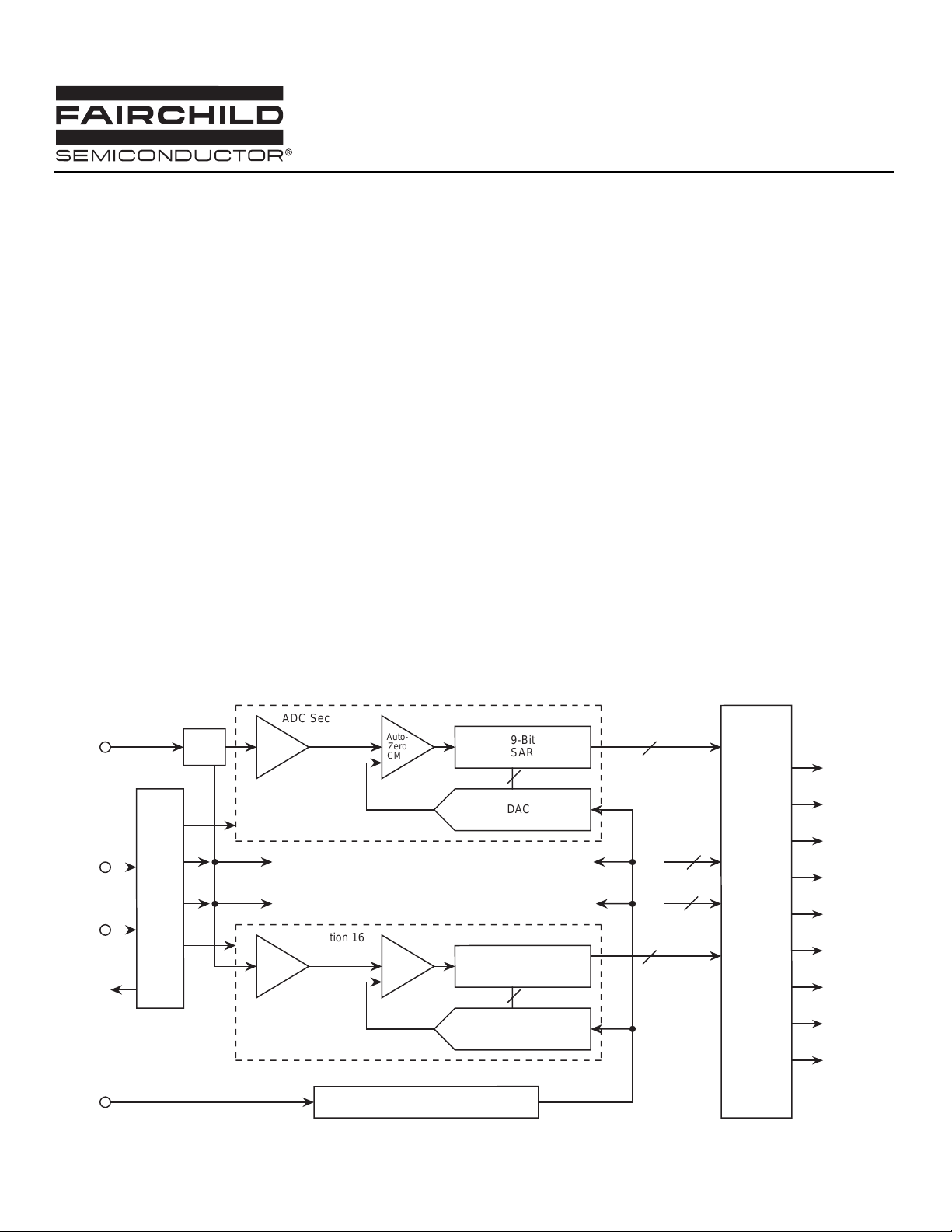
The high sample rate is achieved by using multiple SAR ADC
sections in parallel, each of which samples the input signal in
sequence. Each ADC uses 16 clock cycles to complete a
conversion. The clock cycles are allocated as follows:
Table II - Clock Cycles
Clock Operation
1 Reference zero sampling
2 Auto-zero comparison
3 Auto-calibrate comparison
4 Input sample
5-15 9-bit SAR conversion
16 Data transfer
The 16 phase clock, which is derived from the input clock,
synchronizes these events. The timing signals for adjacent
ADC sections are shifted by one clock cycle so that the analog
input is sampled on every cycle of the input clock by exactly
one ADC section. After 16 clock periods, the timing cycle
repeats. The latency from analog input sample to the corresponding digital output is 12 clock cycles.
FB1
DGND
+5 V
Digital
RTN
10 µF
+D5
+D5
+
+5 V
Digital
FB2
+A5
AGND
+A5
+
10 µF
+5 V
Analog
NOTES: 1) FB3 is to be located as closely to the device as possible.
*To reduce the possibility of latch-up, avoid
connecting the DGND pins of the ADC to the
digital ground of the system.
+5 V
Analog
RTN
2)There should be no additional connections to the right of FB1 and FB2.
3)All capacitors are 0.1 µF surface-mount unless otherwise specified.
4)FB1, FB2 and FB3 are 10 µH inductors or ferrite beads.
FB3
Enable/Tri-State
(Enable = Active Low)
POWER SUPPLIES AND GROUNDING
Fairchild suggests that both the digital and the analog supply
voltages on the SPT7734 be derived from a single analog
supply as shown in figure 1. A separate digital supply should
be used for all interface circuitry. Fairchild suggests using
this power supply configuration to prevent a possible latchup condition on power up.
OPERATING DESCRIPTION
The general architecture for the CMOS ADC is shown in the
block diagram. The design contains 16 identical successive
approximation ADC sections, all operating in parallel, a 16phase clock generator, an 9-bit 16:1 digital output multiplexer, correction logic, and a voltage reference generator
which provides common reference levels for each ADC section.
• Since only 16 comparators are used, a huge power savings
is realized.
• The auto-zero operation is done using a closed loop
system that uses multiple samples of the comparators
response to a reference zero.
• The auto-calibrate operation, which calibrates the gain
of the MSB reference and the LSB reference, is also
done with a closed loop system. Multiple samples of the
gain error are integrated to produce a calibration voltage for
each ADC section.
• Capacitive displacement currents, which can induce sampling error, are minimized since only one comparator
samples the input during a clock cycle.
• The total input capacitance is very low since sections of the
converter which are not sampling the signal are isolated
from the input by transmission gates.
VOLTAGE REFERENCE
The SPT7734 requires the use of a single external voltage
reference for driving the high side of the reference ladder. It
must be within the range of 3 V to 5 V. The lower side of the
ladder is typically tied to AGND (0.0 V), but can be run up to
2.0 V with a second reference. The analog input voltage
range will track the total voltage difference measured between the ladder sense lines, V
RHS
and V
RLS
.
Force and sense taps are provided to ensure accurate and
stable setting of the upper and lower ladder sense line
voltages across part-to-part and temperature variations. By
using the configuration shown in figure 2, offset and gain
errors of less than ±2 LSB can be obtained.
SPT7734
5 1/27/98
Page 6

Figure 2 - Ladder Force/Sense Circuit
R/2
R
R
R
R
R
R
R/2
R=30 Ω (typ)
All capacitors are 0.01 µF
V
RLF
(AGND)
0.0 V
V
RLS
(0.075 V)
V
RHS
(+3.91 V)
90 mV
75 mV
+4.0 V
External
Reference
1
AGND
Figure 3 - Simplified Reference Ladder Drive Circuit
Without Force/Sense Circuit
+
-
-
+
2
V
RHF
3
V
RHS
4 N/C
5
V
RLS
6
V
RLF
7
V
IN
All capacitors are 0.01 µF
In cases where wider variations in offset and gain can be
tolerated, V
tied directly to V
can be tied directly to V
Ref
as shown in figure 3. Decouple force and
RLF
and AGND can be
RHF
sense lines to AGND with a .01 µF capacitor (chip cap
preferred) to minimize high-frequency noise injection. If this
simplified configuration is used, the following considerations
should be taken into account:
The drive requirements for the analog inputs are very minimal
when compared to most other converters due to the SPT7734's
extremely low input capacitance of only 5 pF and very high
input resistance in excess of 50 kΩ.
The analog input should be protected through a series
resistor and diode clamping circuit as shown in figure 4.
The reference ladder circuit shown in figure 3 is a simplified
representation of the actual reference ladder with force and
sense taps shown. Due to the actual internal structure of the
ladder, the voltage drop from V
to the voltage drop from V
RLF
Typically, the top side voltage drop for V
RHF
to V
to V
RLS
is not equivalent
RHS
.
RHF
equal:
V
- V
RHF
and the bottom side voltage drop for V
V
- V
RLS
= 2.25 % of (V
RHS
= 1.9 % of (V
RLF
RHF
RHF
- V
- V
RLF
) (typical),
RLF
to V
RLS
) (typical).
Figure 3 shows an example of expected voltage drops for a
specific case. Vref of 4.0 V is applied to V
to AGND. A 90 mV drop is seen at V
75 mV increase is seen at V
ANALOG INPUT
VIN is the analog input. The input voltage range is from V
to V
respect to the voltage reference. (See voltage reference
section.)
(typically 4.0 V) and will scale proportionally with
RHS
(= 0.075 V).
RLS
and V
RHF
(= 3.91 V) and a
RHS
to V
will equal:
RLF
RLF
RHS
is tied
will
RLS
CALIBRATION
The SPT7734 uses an auto calibration scheme to ensure 8-bit accuracy over time and temperature. Gain and
offset errors are continually adjusted to 8-bit accuracy during
device operation. This process is completely transparent to
the user.
Upon power-up, the SPT7734 begins its calibration algorithm. In order to achieve the calibration accuracy required,
the offset and gain adjustment step size is a fraction of a 8bit LSB. Since the calibration algorithm is an oversampling
process, a minimum of 10,000 clock cycles are required.
This results in a minimum calibration time upon power-up
of 250 µsec (for a 40 MHz clock). Once calibrated, the
SPT7734 remains calibrated over time and temperature.
Since the calibration cycles are initiated on the rising edge of
the clock, the clock must be continuously applied for the
SPT7734 to remain in calibration.
INPUT PROTECTION
All I/O pads are protected with an on-chip protection circuit
shown in figure 5. This circuit provides ESD robustness to
3.5 kV and prevents latch-up under severe discharge condi-
tions without degrading analog transition times.
SPT7734
6 1/27/98
Page 7

Figure 4 - Recommended Input Protection Circuit
+V
D1
AV
DD
DIGITAL OUTPUTS
The digital outputs (D0-D8) are driven by a separate supply
(OVDD) ranging from +3 V to +5 V. This feature makes it
possible to drive the SPT7734's TTL/CMOS-compatible outputs with the user's logic system supply. The format of the
output data (D0-D7) is straight binary. (See table III.) The
outputs are latched on the rising edge of CLK. These outputs
can be switched into a tri-state mode by bringing EN high.
47 Ω
D2
-V
D1 = D2 = Hewlett Packard HP5712 or equivalent
Figure 5 - On-Chip Protection Circuit
V
DD
120 Ω
120 Ω
Pad
ADCBuffer
Table III - Output Data Information
ANALOG INPUT OVERRANGE OUTPUT CODE
D8 D7-D0
+F.S. + 1/2 LSB 1 1111 1111
+F.S. -1/2 LSB O 1111 111Ø
+1/2 F.S. O ØØØØ ØØØØ
+1/2 LSB O OOOO OOOØ
0.0 V O OOOO OOOO
(Ø indicates the flickering bit between logic 0 and 1).
DO NOT CONNECT PINS (DNC)
There are two pins designated as Do Not Connect (DNC).
These pins must be left floating for proper operation of the
Analog
device.
OVERRANGE OUTPUT
The OVERRANGE OUTPUT (D8) is an indication that the
analog input signal has exceeded the positive full scale input
voltage by 1 LSB. When this condition occurs, D8 will switch
to logic 1. All other data outputs (D0 to D7) will remain at
logic 1 as long as D8 remains at logic 1. This feature makes
it possible to include the SPT7734 into higher resolution
systems.
CLOCK INPUT
The SPT7734 is driven from a single-ended TTL-input clock.
Because the pipelined architecture operates on the rising edge of
the clock input, the device can operate over a wide range of input
clock duty cycles without degrading the dynamic performance.
SPT7734
7 1/27/98
Page 8

PACKAGE OUTLINES
32-Lead TQFP
C D
A
B
E F
INCHES MILLIMETERS
G H
I
J
K
L
SYMBOL MIN MAX MIN MAX
A 0.347 0.355 8.90 9.10
B 0.269 0.277 6.90 7.10
C 0.347 0.355 8.90 9.10
D 0.269 0.277 6.90 7.10
E 0.027 0.035 0.68 0.89
F 0.012 0.018 0.30 0.45
G 0.053 0.057 1.35 1.45
H 0.002 0.006 0.05 0.15
I 0.039 typ 1.00 typ
J 0.004 0.008 0.09 0.20
K0° 7° 0° 7°
L 0.018 0.029 0.45 0.75
B
28
1
CD
A
28-Lead SOIC
I H
F
E
INCHES MILLIMETERS
SYMBOL MIN MAX MIN MAX
A 0.696 0.712 17.68 18.08
B 0.004 0.012 0.10 0.30
C .050 typ 0.00 1.27
D 0.014 0.019 0.36 0.48
E 0.009 0.012 0.23 0.30
F 0.080 0.100 2.03 2.54
G 0.016 0.050 0.41 1.27
H 0.394 0.419 10.01 10.64
I 0.291 0.299 7.39 7.59
H
G
SPT7734
8 1/27/98
Page 9

PIN ASSIGNMENTS
PIN FUNCTIONS
V
RLF
V
IN
AGND
AGND
V
CAL
AV
D
D
AV
D
D
DV
Name Function
AGND Analog Ground
V
V
V
V
V
V
AV
DV
RHF
RHS
RLS
RLF
CAL
IN
DD
DD
Reference High Force
Reference High Sense
Reference Low Sense
Reference Low Force
Calibration Reference
Analog Input
Analog V
Digital V
DD
DD
DGND Digital Ground
CLK Input Clock f
EN
Output Enable
=fs (TTL)
CLK
D0-7 Tri-State Data Output, (DØ=LSB)
D8 Tri-State Output Overrange
DAV Data Valid Output
OV
DD
Digital Output Supply
OGND Digital Output Ground
DNC Do Not Connect
AGND
28
D8
27
D7
26
D6
25
D5
24
D4
23
D3
22
OV
DD
21
OGND
20
D2
19
D1
18
D0
17
DNC
16
DNC
15
EN
D6
D8
D7
25
27
26
24
D5
23
D4
22
D3
21
OV
DD
20
OGND
19
D2
18
D1
17
D0
1
AGND
2
V
RHF
3
V
RHS
4
N/C
5
V
RLS
6
V
RLF
7
V
IN
AGND
8
V
9
CAL
10
AV
DD
1
DV
DD
1
DGND
12
CLK
13
DAV
14
V
RLS
32
1
2
3
4
5
6
7
DD
8
V
RHS
31
V
RHF
30
SOIC
AGND
29
TQFP
28
DGND
DV
DD
DGND
CLK
DAV
13
12
10
1
1
9
16
14
15
DNC
EN
DNC
ORDERING INFORMATION
PART NUMBER TEMPERATURE RANGE PACKAGE TYPE
SPT7734SCS 0 to +70 °C 28L SOIC
SPT7734SCT 0 to +70 °C 32L TQFP
DISCLAIMER
FAIRCHILD SEMICONDUCTOR RESERVES THE RIGHT TO MAKE CHANGES WITHOUT FURTHER NOTICE TO ANY PRODUCTS HEREIN TO
IMPROVE RELIABILITY, FUNCTION OR DESIGN. FAIRCHILD DOES NOT ASSUME ANY LIABILITY ARISING OUT OF THE APPLICATION OR USE OF
ANY PRODUCT OR CIRCUIT DESCRIBED HEREIN; NEITHER DOES IT CONVEY ANY LICENSE UNDER ITS PATENT RIGHTS, NOR THE RIGHTS OF
OTHERS.
LIFE SUPPORT POLICY
FAIRCHILD'S PRODUCTS ARE NOT AUTHORIZED FOR USE AS CRITICAL COMPONENTS IN LIFE SUPPORT DEVICES OR SYSTEMS WITHOUT THE
EXPRESS WRITTEN APPROVAL OF THE PRESIDENT OF FAIRCHILD SEMICONDUCTOR CORPORATION. As used herein:
1. Life support devices or systems are devices or systems which, (a) are
intended for surgical implant into the body, or (b) support or sustain life,
and whose failure to perform, when properly used in accordance with
instructions for use provided in the labeling, can be reasonably expected
to result in a significant injury to the user.
www.fairchildsemi.com © Copyright 2002 Fairchild Semiconductor Corporation
2. A critical component is any component of a life support device or system
whose failure to perform can be reasonably expected to cause the failure
of the life support device or system, or to affect its safety or effectiveness.
SPT7734
9 1/27/98
 Loading...