

Page 1
SPT7721
8-BIT, 250 MSPS ADC WITH DEMUXED OUTPUTS
TECHNICAL DATA
NOVEMBER 8, 2001
FEATURES
• TTL/CMOS/PECL compatib le
• High conversion rate: 250 MSPS
• Single +5 V pow er supply
• V ery low pow er dissipation: 310 mW
• Po wer-down mode
• +3.0 V/+5.0 V (LVCMOS) digital output logic
compatibility
• Demuxed output ports
GENERAL DESCRIPTION
The SPT7721 is a high-speed, 8-bit analog-to-digital converter implemented in an advanced BiCMOS process. An
advanced folding and interpolating architecture provides
both a high conversion rate and v ery low power dissipation
of only 310 mW. The analog inputs can be operated in
either single-ended or differential input mode. A 2.5 V common mode reference is provided on chip for the singleended input mode to minimize external components.
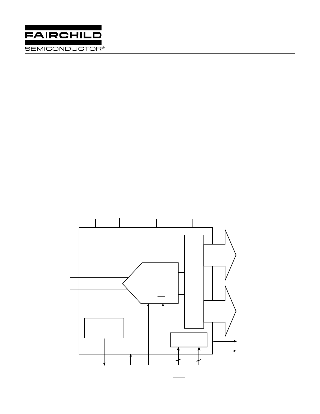
BLOCK DIAGRAM
AGND DGND
AV
APPLICATIONS
• RGB video processing
• Digital communications
• High-speed instrumentation
• Projection display systems
The SPT7721 digital outputs are demuxed (double-wide)
with both dual-channel and single-channel selectable output modes. Demuxed mode supports either parallel
aligned or interleaved data output. The output logic is both
+3.0 V and +5.0 V compatible. The SPT7721 is av ailable in
a 44-lead TQFP surf ace mount package ov er the industrial
temperature range of –40 to +85 °C.
CC
OV
DD
V
IN
VIN
DA0DA
+
8-Bit
7
250 MSPS
ADC
CLK CLK
Common Mode
Voltage
Reference
+2.5 V
V
CM
PD CLK
CLK
Data Output Latches
Data Output
Mode Control
22
Reset
Reset
DMODE
&
DB0DB
DCLK
DCLK
1,2
7
OUT
OUT
Page 2

ABSOLUTE MAXIMUM RATINGS (Beyond which damage may occur) 25 °C
Supply V oltages
AVCC...................................................................... +6 V
OVDD..................................................................... +6 V
Input V oltages
Analog Inputs ............................... –0.5 V to VCC +0.5 V
Digital Inputs ................................ –0.5 V to V
+0.5 V
CC
T emperatures
Operating Temperature ........................... –40 to +85 °C
Storage Temper ature............................ –65 to +125 °C
Note: Operation at any Absolute Maximum Rating is not implied.
See Electrical Specifications for proper applied conditions in
typical applications.
ELECTRICAL SPECIFICATIONS
TA = T
PARAMETERS CONDITIONS LEVEL MIN TYP MAX UNITS
Resolution 8 Bits
DC Performance ƒIN = 1 kHz
Analog Input
to T
, AV
MIN
MAX
= +5.0 V, ƒ
CC
= 250 MHz, VCM = 2.5 V, OVDD = 5.0 V, unless otherwise specified.
CLK
TEST TEST SPT7721
Differential Linearity Error (DLE) +25 °C V –0.70/+1.05 LSB
–40 °C to +85 °C V –0.95/+1.5 LSB
Integral Linearity Error (ILE) +25 °C V ±1.7 LSB
Best Fit –40 °C to +85 °C V ±2.25 LSB
No Missing Codes +25 °C, ƒ
= 1 kHz I Guaranteed
IN
Input V oltage Range
(with respect to V
–) +25 °C V ±470 mV
IN
P-P
Gain Variation VI 2 %
Input Common Mode (VCM) IV 2.3 2.5 3.0 V
Input Bias Current VI 10 µA
Input Resistance +25 °C V 50 kΩ
Input Capacitance +25 °C V 4 pF
Input Bandwidth +25 °C (–3 dB of FS) V 220 MHz
Offset Error VI ±10 mV
Offset Power Supply Rejection Ratio V 0.5 mV/V
Timing Characteristics
Maximum Conversion Rate VI 250 MSPS
Output Delay (Clock-to-Data) (t
) –40 °C to +85 °C IV 6 8 10.5 ns
pd1
Output Delay Tempco V 22 ps/°C
Aperture Delay Time (t
) IV 0.5 ns
ap
Aperture Jitter Time IV 2 ps rms
Pipeline Delay (Latency)
Single Channel Mode V 2.5 Clocks
Demuxed Interleaved Mode V 2.5 Clocks
Demuxed Parallel Mode
Channel B V 2.5 Clocks
Channel A V 3.5 Clocks
CLK to DCLK
Single Channel Mode (t
Dual Channel Mode (t
Delay Time
OUT
) IV467ns
pd2
) IV 5.3 6.16 7.8 ns
pd3
Dynamic Performance
Effective Number of Bits (ENOB)
= 70 MHz +25 °C VI 5.8 6.4 Bits
ƒ
IN
= 70 MHz –40 °C to +85 °C IV 5.5 6.0 Bits
ƒ
IN
Signal-to-Noise Ratio (SNR)
= 70 MHz +25 °C VI 42 43 dB
ƒ
IN
ƒIN = 70 MHz –40 °C to +85 °C IV 36 40 dB
SPT7721
2 11/8/01
Page 3

ELECTRICAL SPECIFICATIONS
TA = T
MIN
to T
MAX
, AV
= +5.0 V, ƒ
CC
= 250 MHz, VCM = 2.5 V, OVDD = 5 V, unless otherwise specified.
CLK
TEST TEST SPT7721
PARAMETERS CONDITIONS LEVEL MIN TYP MAX UNITS
Dynamic Performance
Total Harmonic Distortion (THD)
= 70 MHz +25 °C VI –43 –40 dB
ƒ
IN
= 70 MHz –40 °C to +85 °C IV –42 –37 dB
ƒ
IN
Signal-to-Noise and Distortion (SINAD)
= 70 MHz +25 °C VI 3 7 40 dB
ƒ
IN
= 70 MHz –40 °C to +85 °C IV 35 38 dB
ƒ
IN
Power Supply Requirements
Voltage (Analog Supply) IV 4.75 5.0 5.25 V
AV
CC
OVDD Voltage (Digital Supply) IV 2.75 5.25 V
Current VI 62 70 mA
AV
CC
Power Dissipation with Inter nal Voltage Reference VI 310 3 50 mW
Common Mode Reference
Voltage VI 2.45 2.5 2.55 V
Voltage Tempco V 100 ppm/°C
Output Impedance I
= ±50 µA V 1 kΩ
OUT
Power Supply Rejection Ratio V 63 mV/V
Clock and Reset Inputs (Differential and Single-Ended)
Differential Signal Amplitude (V
Differential High Input Voltage (V
Differential Low Input Voltage (V
DIFF)
IHD)
ILD)
Differential Common-Mode Input (V
Single-Ended High Input Voltage (V
Single-Ended Low Input Voltage (V
Input Current High (II
Input Current Low (II
H)
L)
CMD)
IH)
IL)
VID = 1.5 V VI –100 20 +100 µA
VID = 1.5 V VI –100 20 +100 µA
VI 400 mV
IV 1.4 5 V
IV 0 3.9 V
IV 1.2 4.1 V
IV 1.8 V
IV 1.2 V
P-P
Power Down and Mode Control Inputs (Single-Ended)
High Input Voltage IV 2.0 AV
CC
V
Low Input Voltage IV 0 1.0 V
Maximum Input Current Low VI –100 10 +100 µA
Maximum Input Current High <4.0 V VI –100 10 +100 µA
Digital Outputs
Logic "1" Voltage I
Logic "0" Voltage I
OH
OL
TR/TF Data 10 pF load
OV
OV
TR/TF DCLK = (10 pF load)
OV
OVDD = 5 V V 0.7 ns
TEST LEVEL CODES
All electrical characteristics are subject to the
following conditions:
All parameters having min/max specifications
are guaranteed. The Test Level column indicates the specific device testing actually performed during production and Quality Assurance inspection. Any blank section in the data
column indicates that the specification is not
tested at the specified condition.
= –0.5 mA VI OVDD – 0.2 OVDD – 0.06 V
= +1.6 mA VI 0.13 0.2 V
= 3 V V 3.5 ns
DD
= 5 V V 2.0 ns
DD
= 3 V V 1.3 ns
DD
LEVEL TEST PROCEDURE
I 100% production tested at the specified temperature.
II 100% production tested at T
= +25 °C, and sample tested at the
A
specified temperatures.
III QA sample tested only at the specified temperatures.
IV Parameter is guaranteed (but not tested) by design and characteri-
zation data.
V Parameter is a typical value for information purposes only.
VI 100% production tested at TA = +25 °C. Parameter is guaranteed
over specified temperature range.
SPT7721
3 11/8/01
Page 4
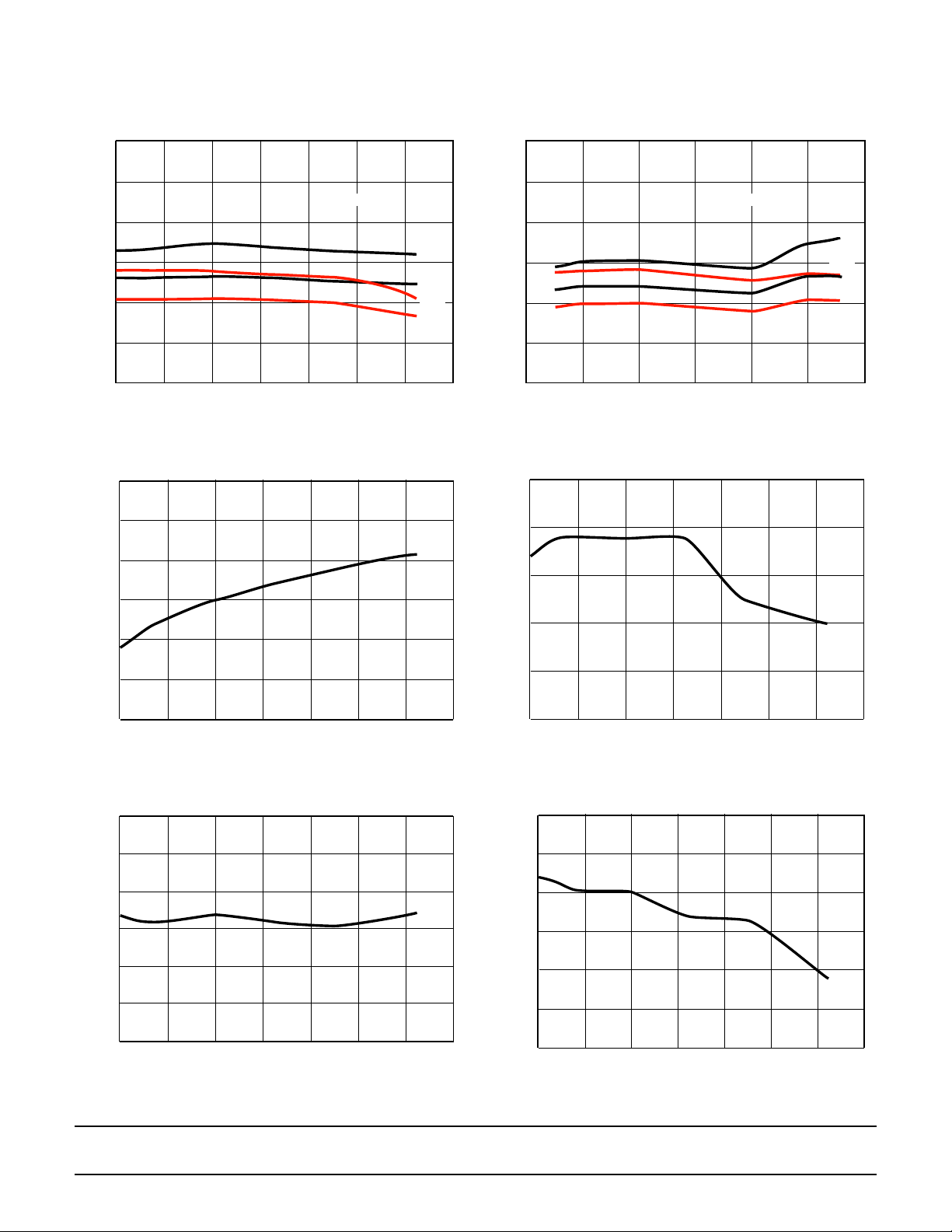
TYPICAL PERFORMANCE CHARACTERISTICS
AC Perf ormance vs Temperature
60
55
50
45
40
35
SFDR, THD, SNR, SINAD (dB)
30
40
75
70
65
(mA)
60
CC
AV
55
20
0
20
Temperature (°C)
AV
Current vs Temperature
CC
IN = 70 MHz
40
60 80
SFDR
THD
SNR
SINAD
100
AC P erf ormance vs Sample Rate
60
55
IN = 70 MHz
50
45
40
35
SFDR, SNR, THD, SINAD (dB)
30
0
50
100
150
200
Sample Rate (MSPS)
AVCC Current Power Do wn vs Temperature
3.0
2.8
2.6
(mA)
CC
2.4
AV
SFDR
SNR
THD
SINAD
250 300
50
45
6.0
4.0
2.0
0.0
mV
2.0
4.0
6.0
2.2
40
20
0
20
40
Temperature (°C)
60 80
100
2.0
40
20
0
20
40
Temperature (°C)
V olta ge Offset Error vs Temperature Percent Gain Error vs Temperature
1.06
1.05
1.04
1.03
%
1.02
1.01
40
20
0
20
40
Temperature (°C)
60 80
100
1.00
40
20
0
20
40
Temperature (°C)
60 80
60 80
100
100
SPT7721
4 11/8/01
Page 5

TYPICAL PERFORMANCE CHARACTERISTICS
Input Bandwidth Common-Mode Reference V oltage vs V
1
0
1
2
dB
3
4
5
100
0
200
300
400
500 600
Input Frequency (MHz)
OVDD Current vs Clock Frequency, Dual Mode
120
100
Output VDD=5 V
80
60
mA
40
Output VDD=3 V
CC
2.50
2.49
2.48
2.47
V
2.46
OUT
2.45
2.44
VCM
2.43
2.42
2.41
2.40
4.5
4.7
4.9
5.1
5.3
5.5
VCC V
OVDD Current vs Clock Frequency, Single Mode
60
50
40
30
mA
20
Output VDD=5 V
Output VDD=3 V
5.7
20
0
0
50
100
Clock Frequency (MHz)
T otal Power vs Clock Frequency
1000
800
700
600
500
400
Power Dissipation (mW)
300
0
50
with 6 pF loads
100
Clock Frequency (MHz)
150
150
200
200
250 300
OVDD=5 V
OVDD=3 V
250 300
10
0
0
25
50
75
100
125 150
Clock Frequency (MHz)
Differential Input Common-Mode Operating Range
6
5
4
3
Volts
2
1
0
50
400 mV
Common-Mode Operating Range
40
20
0
20
P-P
40
60 80
Temperature (°C)
100
SPT7721
5 11/8/01
Page 6

THEORY OF OPERATION
The SPT7721 is a three-step subranger. It consists of two
THAs in series at the input, followed by three ADC b locks .
The first block is a three-bit folder with over/under range
detection. The second b lock consists of two single-bit f olding interpolator stages. There are pipelining THAs between
each ADC block.
The analog decode functions are the input buffer, input
THAs, three-bit folder , f olding interpolators, and pipelining
THAs. The input buffer enables the part to withstand railto-rail input signals without latchup or excessive currents
and also performs single-ended to differential conv ersion.
All of the THAs have the same basic architecture. Each
has a differential pair buffer followed by switched emitter
followers driving the hold capacitors. The input THA also
has hold mode feedthrough cancellation de vices.
The three MSBs of the ADC are generated in the first
three-bit folder block, the output of which driv es a differential reference ladder which also sets the full-scale input
range. Differential pairs at the ladder taps generate
midscale, quarter and three-quarter scale, overr ange, and
underrange. Every other differential pair collector is crosscoupled to generate the eighth scale zero crossings. The
middle ADC block generates two bits from the folded signals of the previous stages after pipeline THAs. Its outputs
drive more pipeline THAs to push the decoding of the three
LSBs to the next half clock cycle . The three LSBs are generated in interpolators that are latched one full clock cycle
after the MSBs.
The digital decode consists of comparators, exclusive of
cells for gray to binary decoding, and/or cells used for
mostly over/under range logic. There is a total of 3.5 cloc k
cycles latency before the output bank selection. In order to
reduce sparkle codes and maintain sample rate, no more
than three bits at a time are decoded in any half clock
cycle.
The output data mode is controlled by the state of the
demux mode inputs. There are three output modes .
• All data on bank A with clock r ate limited to one-half
maximum
• Interleav ed mode with data alternately on banks A and
B on alternate clock cycles
• Parallel mode with bank A delayed one cycle to be
synchronous with bank B every other clock cycle
If necessary , the input clock is divided b y tw o. The divided
clock selects the correct output bank. The user can synchronize with the divided clock to select the desired output
bank via the differential RESET input.
The output logic family is L VCMOS with output VDD supply
adjustable from 2.7 volts to 5.3 v olts. There are also differential clock output pins that can be used to latch the output
data in single bank mode or to indicate the current output
bank in demux mode.
Finally , a pow er-down mode is availab le, which causes the
outputs to become tri-state, and overall power is reduced
to about 10 mW . There is a 2.5 V reference to supply common mode for single-ended inputs that is not shut down in
power-down mode .
Figure 1 – Single Mode Timing Diagram
2.5 CLK Cycles of Latency
N+1
t
pd2
V
IN
CLK
/CLK
D0D7
(Port A)
DCLKOUT
/DCLKOUT
t
N
pd2
t
ap
N+2
t
pd1
N1N2N3 N
N+3
N+4
N+1
N+5
N+2
SPT7721
6 11/8/01
Page 7

Figure 2 – Dual Mode Timing Diagram
U6-Reset
Refer to AN7722
DCLKOUT
/DCLKOUT
U6-Reset
Refer to AN7722
Vin
/CLK
CLK
/Reset
Reset
Port A
Port B
Port A
Port B
Vin
/CLK
CLK
/Reset
Reset
tpd2
N-6
N-7
N-6
N-2
N-2
tap
tap
N-5
N-1
550ps
N-1
550ps
tpd3
2.5 CLK Cycles of Latency
N
550ps
treset
ts
tpd1
INTERLEAVED DATA OUTPUT
N-4
PARALLEL DATA OUTPUT
N-5
N-4
tpd2
N
550ps
treset
ts
tpd1
N+1
Invalid Data
N+2
N-2
N-2
2.5 CLK Cycles of Latency
N+1
N+2
tpd1
tpd1
N-1
N+3
N+3
N+4
tpd1
N+1
N
N-1Invalid Data
N
N+4
tpd1
Port A
Port B
Port A
Port B
/DCLKOUT
DCLKOUT
N-6
N-4
N-5
tpd2
N-6
N-5
Data Output Possibilities w/o Reset
INTERLEAVED DATA OUTPUT
Invalid Data
PARALLEL DATA OUTPUT
tpd1
7 11/8/01
N-2
Invalid Data
N-2
N-1
N+1
N
N-1
N
SPT7721
Page 8

Figure 3 – Typical Interface Cir cuit
T1
A
IN
Mini-Circuit
T1-6T
.01
Mode
Select
OUT
1 (2)
CC
AV
DMode1
2 (2)
CC
AV
VCM
VIN+
50
V
IN
Reset
Diff In
Reset
DMode2
SPT7721
AGND1 (4)
AGND2 (2)
Reset
Clock
Diff In
CLK
DA0DA
DCLK
DCLK
DB0DB
DGND (3)
CLK
(3)
OV
OUT
OUT
DD
7
Interfacing
Logics
7
Notes:
1) FB = Ferrite bead. It must placed as close to the ADC as possible.
2) All inputs are internally biased:
a) DMode1 to GND through 100K
b) DMode2 to VCC through 50K
c) CLK, PD and Rest pins to GND through 100K
d) /CLK and /Reset pins to 1.5 V through 5K
e) V
+ and VIN to +2.5 V through 50K
IN
3) All 0.01microfarad capacitors are surface mount caps. They must be
placed as close to the respective pin as possible
Default = interleave dual
}
channel output
.01(2x)
TYPICAL INTERFACE CIRCUIT
V ery few e xternal components are required to achiev e the
stated device performance. Figure 3 shows the typical
interface requirements when using the SPT7721 in normal
circuit operation. The following sections provide descriptions of the major functions and outline performance
criteria to consider for achieving the optimal device
performance.
ANALOG INPUT
The input of the SPT7721 can be configured in various
ways depending on whether a single-ended or differential
input is desired.
The AC-coupled input is most conveniently implemented
using a transformer with a center-tapped secondary winding. The center tap is connected to the VCM pin as shown in
figure 3. To obtain low distortion, it is impor tant that the
selected transformer does not exhibit core saturation at
the full-scale voltage. Proper termination of the input is important for input signal purity. A small capacitor across the
input attenuates kickback noise from the internal trackand-hold.
Figure 4 illustrates a solution (based on operational amplifiers) that can be used if a DC-coupled single-ended input
is desired. It is v ery important to select op amps with a high
open-loop gain, a bandwidth high enough so as not to impair the performance of the ADC, low THD , and high SNR.
.01(3x)
+A5
.01(3x)
+
10
FB
+
10
+D3/5
+D3/5
Figure 4 – DC-Coupled Single-Ended to Differential
Conversion (power supplies and bypassing
are not shown)
V
CM
Input
Voltage
(±0.5 V)
R3
(R3)/2
R3
+
R
R2
R2
51 W
R
RR
R
+
+
51 W
15 pF
51 W
INPUT PROTECTION
All I/O pads are protected with an on-chip protection
circuit. This circuit provides ESD robustness and prevents
latchup under severe discharge conditions without
degrading analog transmission times.
POWER SUPPLIES AND GR OUNDING
The SPT7721 is operated from a single power supply in
the range of 4.75 to 5.25 volts. Nor mal operation is suggested to be 5.0 volts. All po wer supply pins should be b ypassed as close to the package as possible. The analog
and digital grounds should be connected together with a
ferrite bead as shown in the typical interface circuit and as
close to the ADC as possible.
ADC
V
V
+
IN
IN
SPT7721
8 11/8/01
Page 9

POWER DO WN MODE
DIGITAL OUTPUTS
To save on power, the SPT7721 incorporates a powerdown function. This function is controlled by the signal on
pin PD. When pin PD is set high, the SPT7721 enters the
power-down mode . All outputs are set to high impedance.
In the power-down mode the SPT7721 dissipates 10 mW
typically.
REFERENCES
To save on parts count, design time, and PC board real
estate, the SPT7721 utilizes an internal reference. No
other external components are required to implement this
feature.
COMMON MODE VOLTAGE REFERENCE CIRCUIT
The SPT7721 has an on-board common-mode voltage
reference circuit (VCM). It is 2.5 v olts and is capable of driving 50 µA loads typically. The circuit is commonly used to
drive the center tap of the RF transformer in fully differential applications. For single-ended applications, this output
can be used to provide the level shifting required for the
single-to-differential conv erter conversion circuit.
CLOCK INPUT
The clock input on the SPT7721 can be driven by either a
single-ended or double-ended clock circuit and can handle
TTL, PECL, and CMOS signals. When operating at high
sample rates it is important to keep the pulse width of the
clock signal as close to 50% as possible. For TTL/CMOS
single-ended clock inputs, the rise time of the signal also
becomes an important consideration.
The output circuitry of the SPT7721 has been designed to
be able to support three separate output modes. The
demuxed (double-wide) mode supports either parallel
aligned or interleaved data output. The single-channel
mode is not demuxed and can support direct output at
speeds up to 125 MSPS. The output format is straight
binary (table I).
Table I – Output Data Format
Analog Input Output Code
+FS 1111 1111
+FS – 1/2 LSB 1111 111Ø
+1/2 FS ØØØØ ØØØØ
–FS + 1/2 LSB 0000 000Ø
–FS 0000 0000
Ø indicates the flickering bit between logic 0 and 1
D7–D0
The data output mode is set using the DMODE1 and
DMODE2 inputs (pins 32 & 31 respectively). Table II
describes the mode switching options.
Table II – Output Data Modes
Output Mode DMODE1DMODE
Parallel Dual Channel Output 0 0
Interleaved Dual Channel Output 0 1
Single Channel Data Output
(Bank A only 125 MSPS max) 1 X
2
EVALUATION BOARD
The EB7721/22 evaluation board is a vailable to aid designers in demonstrating the full performance of the SPT7721.
This board includes a clock driver and reset circuit, adjustable references and common mode , a single-ended to differential input buffer and a single-ended to differential
transformer (1:1). An application note (AN7721/22) describing the operation of this board, as well as information
on the testing of the SPT7721, is also available. Contact
the factory for price and availability of the EB7721/22.
SPT7721
9 11/8/01
Page 10

PACKAGE OUTLINE
44-Lead TQFP
A
B
INCHES MILLIMETERS
SYMBOL MIN MAX MIN MAX
A 0.472 Typ 12.00 Typ
Pin 1
Index
B 0.394 Typ 10.00 Typ
C 0.394 Typ 10.00 Typ
D 0.472 Typ 12.00 Typ
E 0.031 Typ 0.80 Typ
C
D
F 0.012 0.018 0.300 0.45
G 0.053 0.057 1.35 1.45
H 0.002 0.006 0.05 0.15
I 0.020 0.030 0.500 0.750
J 0.039 Typ 1.00 Typ
K 0-7° 0-7°
E F
G
K
H
I
J
SPT7721
10 11/8/01
Page 11

PIN ASSIGNMENTS
DA
AGND
CLK
CLK
RESET
RESET
OV
DGND
7
(MSB)
DA
DA
PD
AV
CCAVCC
43
3
AGND
41
42
SPT7721
TOP VIEW
44L TQFP
DA2DA
1
AGND
44
1
2
3
4
5
6
DD
6
5
7
8
9
10
11
1213141516
DA4DA
V
IN
+
40
DA
0
(LSB)
V
IN
39
171918
OV
DD
AGND
38
DGND
V
CM
37
DB
0
(LSB)
AV
AV
CC
CC
35
36
202221
DB
1DB2DB3
AGND
34
33
32
31
30
29
28
27
26
25
24
23
PIN FUNCTIONS
Pin Name Description
VIN+ Non-Inverted Analog Input; nominally 1 V
100k pullup to V
internally
VIN– Inverted Analog Input; nominally 1 V
pullup to V
CC
internally
DA
–DA
0
Data output; Bank A. 3 V / 5 V LVCMOS
7
compatible.
and 100k pulldown to AGND,
CC
; 100k
P-P
and 100k pulldown to AGND,
AGND
DMODE
DMODE
OV
DGND
DCLK
DCLK
DB
DB
DB
DB
P-P
DD
(MSB)
7
6
5
4
;
DB0–DB
Data output; Bank B. 3 V / 5 V LVCMOS
7
compatible.
DCLK
OUT
Non-Inverted data output clock. 3 V / 5 V
LVCMOS compatible.
DCLK
OUT
Inverted data output clock. 3 V / 5 V LVCMOS
compatible.
CLK Non-Inverted clock input pin; 100k pulldown to
1
2
CLK Inverted clock input pin; 17.5k pullup to VCC and
AGND, internally
7.5k pulldown to AGND, inter nally
RESET RESET synchronizes the data sampling and data
OUT
OUT
output bank relationship when in Dual Channel
Mode (DMODE
= 0); 100k pulldown to AGND,
1
internally
RESET Inverted RESET input pin; 17.5k pullup to V
and 7.5k pulldown to AGND, inter nally
DMODE
1,2
Internally:
100k pulldown to AGND on DMODE1
50k pullup to V
on DMODE2
CC
Data Output Mode pins:
DMODE
= 0, DMODE2 = 0: Parallel Dual
1
Channel Output
DMODE
= 0, DMODE2 = 1: Interleaved Dual
1
Channel Output
DMODE
= 1, DMODE2 = X: Single Channel
1
Data Output on Bank A (125 MSPS max)
PD Power Down pin; PD = 1 for power-down mode.
Outputs set to high impedance in power-down
mode; 100k pulldown to AGND, internally
V
AV
OV
CM
CC
DD
2.5 V Common Mode Voltage Reference Output
+5 V Analog Supply
+3 V / +5 V Digital Output Supply
AGND Analog Ground
DGND Digital Ground
CC
ORDERING INFORMATION
PART NUMBER TEMPERATURE RANGE PACKAGE
SPT7721SIT –40 to +85 °C 44L TQFP
DISCLAIMER
FAIRCHILD SEMICONDUCTOR RESERVES THE RIGHT TO MAKE CHANGES WITHOUT FURTHER NOTICE TO ANY PRODUCTS HEREIN TO
IMPROVE RELIABILITY, FUNCTION OR DESIGN. FAIRCHILD DOES NOT ASSUME ANY LIABILITY ARISING OUT OF THE APPLICATION OR
USE OF ANY PRODUCT OR CIRCUIT DESCRIBED HEREIN; NEITHER DOES IT CONVEY ANY LICENSE UNDER ITS PATENT RIGHTS, NOR
THE RIGHTS OF OTHERS.
LIFE SUPPORT POLICY
FAIRCHILD'S PRODUCTS ARE NOT AUTHORIZED FOR USE AS CRITICAL COMPONENTS IN LIFE SUPPORT DEVICES OR SYSTEMS
WITHOUT THE EXPRESS WRITTEN APPROVAL OF THE PRESIDENT OF FAIRCHILD SEMICONDUCTOR CORPORATION. As used herein:
1. Life support devices or systems are devices or systems which, (a) are
intended for surgical implant into the body, or (b) support or sustain life,
and whose failure to perform, when properly used in accordance with
instructions for use provided in the labeling, can be reasonably
expected to result in a significant injury to the user.
www.fairchildsemi.com © Copyright 2002 Fairchild Semiconductor Corporation
2. A critical component is any component of a life support device or
system whose failure to perform can be reasonably expected to cause
the failure of the life support device or system, or to affect its safety or
effectiveness.
SPT7721
11 11/8/01
 Loading...