

Page 1
FEATURES
SPT7720
8-BIT, 200 MSPS A/D CONVERTER
TECHNICAL DATA
MAY 9, 2001
APPLICATIONS
• Pin-compatible with AD9054
• High conversion rate: 200 MSPS
• Less than ±1/2 LSB DLE
• 7.16 effective number of bits (ENOB) at 70 MHz
• Single +5 V power supply
• Internal THA and voltage reference
• Low power: 430 mW
• 500 MHz full-power bandwidth
•1 VPP input range
• Single or demuxed TTL output ports
• 44-lead TQFP
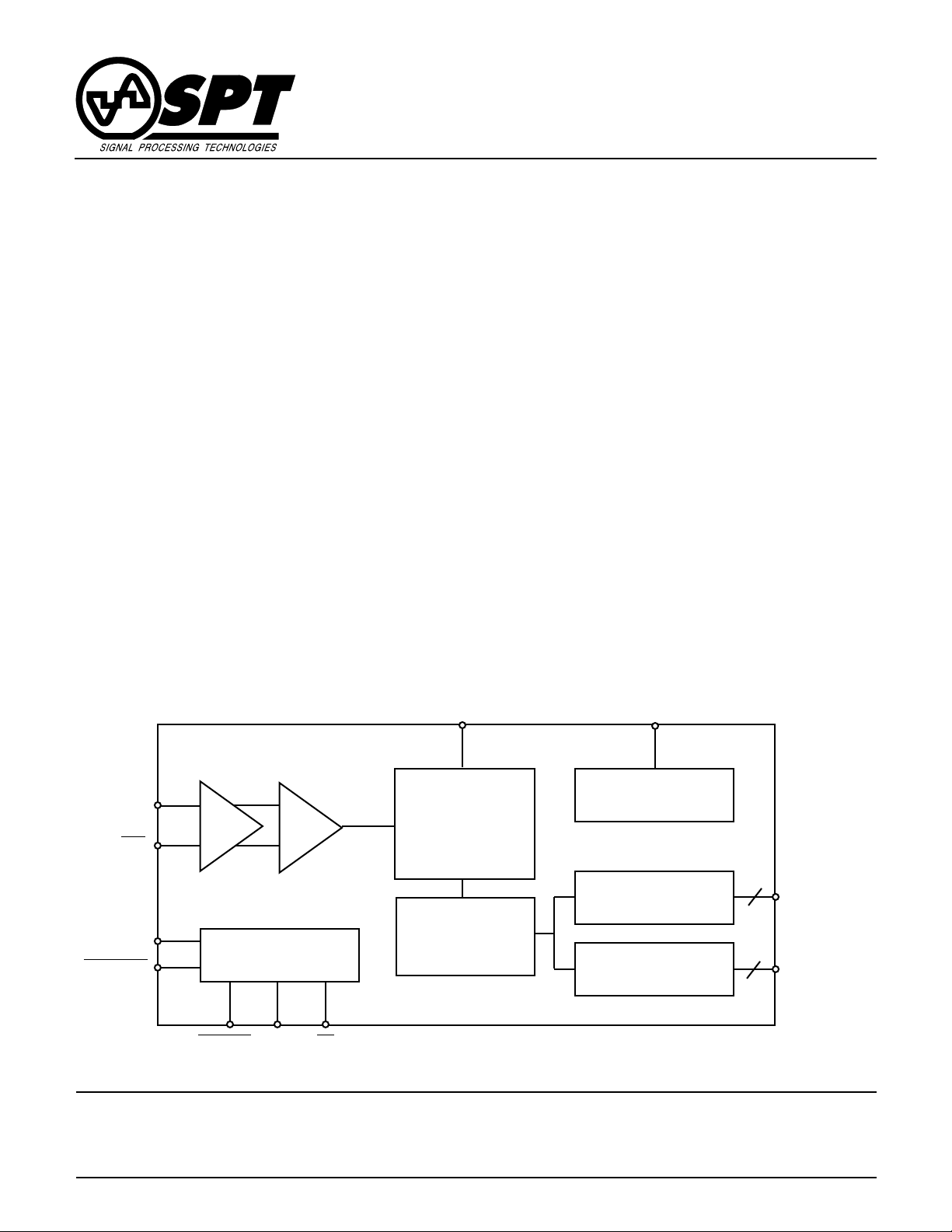
GENERAL DESCRIPTION
The SPT7720 is an 8-bit, high-speed, analog-to-digital
converter implemented in a 0.5 µm BiCMOS process. It
utilizes a folding and interpolating architecture that provides both high sample rates and low power. The device
comes complete with a high bandwidth track-and-hold
amplifier and internal voltage reference.
BLOCK DIAGRAM
V
REF
• Digital sampling oscilloscopes (DSO)
• RGB video processing
• Digital communications
• High-speed instrumentation
• Projection display systems
The SPT7720 digital inputs interface directly to TTL,
CMOS or positive ECL (PECL) logic. The digital outputs
are user selectable in either single-channel or dual-channel modes. It is a pin-compatible, direct replacement for
the AD9054. The SPT7720 is availab le in a 44-lead TQFP
surface mount package over the industrial temperature
range of –40 to +85 °C.
V
IN
REF
OUT
AIN
AIN
+
THA
Quantizer
Reference
8
Channel A
Binary
ENCODE
ENCODE
Timing & Control
DEMUX
DSDS
Encoder
Channel B
8
Signal Processing Technologies, Inc.
4755 Forge Road, Colorado Springs, Colorado 80907, USA
Phone: 719-528-2300 Fax: 719-528-2370 Web Site: http://www .spt.com e-mail: sales@spt.com
DA
DA
7
DB7 DB
0
0
Page 2

ABSOLUTE MAXIMUM RATINGS (Beyond which damage may occur)1 25 °C
Supply Voltages
VDD........................................................................+6 V
Input Voltages
Analog Inputs ............................................... 0.0 to V
Digital Inputs ................................................ 0.0 to V
V
REFL
, V
................................................ 0.0 to V
REFH
Temperatures
Operating T emper ature .......................... –40 to +85 °C
Storage Temperature............................–65 to +125 °C
DD
Note 1. Operation at any Absolute Maximum Rating is not implied. See
DD
DD
Electrical Specifications for proper nominal applied conditions in
typical applications.
ELECTRICAL SPECIFICATIONS
TA=T
to T
MIN
PARAMETERS CONDITIONS LEVEL MIN TYP MAX UNITS
DC Accuracy
Differential Linearity Error (DLE) +25 °C I ±0.41 ±0.75 LSB
Integral Linearity Error (ILE) +25 °C I ±0.56 ±1.0 LSB
No Missing Codes VI Guaranteed
Gain Error +25 °C I ±1.06 ±1.08 %FS
Gain Tempco V 0 ppm/°C
Switching Performance
Encode Pulsewidth High +25 °C IV 2.125 15 ns
Encode Pulsewidth Low +25 °C IV 2.125 15 ns
Aperture Delay (t
Aperture Uncer tainty (Jitter) & Noise +25 °C V 4.5 ps rms
Data Sync Setup Time (t
Data Sync Hold Time (t
Data Sync Pulsewidth Time (t
Output Valid Time (t
Output Prop. Delay (tPD) IV 6.7 8.0 ns
, VDD=+5.0 V , external reference, ƒS=200 MSPS, input amplitude = –1 dBFS, unless otherwise noted
MAX
TEST TEST SPT7720
–40 °C to +85 °C V ±1.0 ±1.0 LSB
–40 °C to +85 °C V ±0.9 ±1.2 LSB
) +25 °C V 0.57 ns
A
) +25 °CIV0 ns
SDS
) +25 °C IV 0.5 ns
HDS
) IV 4.4 5.7 ns
V
) +25 °C IV 2.0 ns
PWDS
Dynamic Performance
Transient Response +25 °C V 1.5 ns
Overvoltage Recovery Time +25 °C V 1.5 ns
Signal-to-Noise Ratio (SNR)
(without harmonics)
= 19.7 MHz +25 °CV 47dB
ƒ
IN
= 19.7 MHz –40 °C to +85 °CV 47 dB
ƒ
IN
ƒIN = 70.1 MHz +25 °C I 44 46.3 dB
= 70.1 MHz –40 °C to +85 °C V 45.8 dB
ƒ
IN
Signal-to-Noise Ratio and Distortion
(SINAD)
= 19.7 MHz +25 °CV 47dB
ƒ
IN
= 19.7 MHz –40 °C to +85 °CV 43 dB
ƒ
IN
ƒIN = 70.1 MHz +25 °C I 43 44.9 dB
= 70.1 MHz –40 °C to +85 °C V 44.5 dB
ƒ
IN
2nd Harmonic Distortion
= 19.7 MHz +25 °CV –59 dBc
ƒ
IN
= 70.1 MHz +25 °CV –55.4 dBc
ƒ
IN
3rd Harmonic Distor tion
= 19.7 MHz +25 °CV –58 dBc
ƒ
IN
= 70.1 MHz +25 °CV –56.4 dBc
ƒ
IN
Total Harmonic Distortion (THD)
= 70.1 MHz +25 °CI –50.9 –46.0 dBc
ƒ
IN
= 70.1 MHz –40 to +85 °CV –48.3 dBc
ƒ
IN
Effective Number of Bits (ENOB)
= 70.1 MHz +25 °C I 6.9 7.16 Bits
ƒ
IN
ƒIN = 70.1 MHz –40 to +85 °C V 6.5 Bits
SPT
SPT7720
2 5/9/01
Page 3

ELECTRICAL SPECIFICATIONS
TA=T
to T
MIN
PARAMETERS CONDITIONS LEVEL MIN TYP MAX UNITS
Analog Input
Input Voltage Range (differential) V ±0.5 V
Compliance Range V 1.8 3.2 V
Input Offset Voltage +25 °C I ±4 ±16 mV
Input Offset Voltage –40 °C to +85 °C V ±8 ±19 mV
Input Resistance +25 °C V 36 62 kΩ
Input Capacitance V 4 pF
Input Bias Current +25 °C I 11 50 µA
Input Bias Current –40 °C to +85 °CV 75µA
Full Power Bandwidth V 500 MHz
Reference Output Voltage VI 2.4 2.5 2.6 V
Temperature Coefficient V 110 ppm/°C
Differential Digital Inputs
High Level Current –40 to +85 °C V 500 625 µA
Low Level Current –40 to +85 °C V 500 625 µA
Input Capacitance V 3 pF
Differential Inputs
Differential Signal Amplitude IV 400 mV
High Input Voltage I V 1.5 V
Low Input Voltage IV 0 V
Common-Mode Input Voltage IV 1.5 V
, VDD=+5.0 V , external reference, ƒS=200 MSPS, input amplitude = –1 dBFS, unless otherwise noted
MAX
TEST TEST SPT7720
>1.5 V differential
>1.5 V differential
DD
–0.4 V
DD
V
Demux Input
High Input Voltage V I 2.0 V
Low Input Voltage VI 0 0 .8 V
Digital Outputs
High Output Voltage Source 800 µA VI 2.4 3. 9 V
Low Output Voltage Sink 1.6 mA VI 0.8 0 .4 V
Output Coding Binary
Power Supply
Supply Current –40 to +85 °C VI 86 111 mA
V
DD
Power Dissipation VI 430 555 mW
Power Supply Sensitivity +25 °C IV 0.005 0.015 V/V
TEST LEVEL CODES
All electrical characteristics are subject to the
following conditions:
All parameters having min/max specifications
are guaranteed. The Test Level column indicates
the specific device testing actually performed
during production and Quality Assurance
inspection. Any blank section in the data column
indicates that the specification is not tested at
the specified condition.
TEST LEVEL
I
II
III
IV
V
VI
TEST PROCEDURE
100% production tested at the specified temperature.
100% production tested at TA = +25 °C, and sample tested at
the specified temperatures.
QA sample tested only at the specified temperatures.
Parameter is guaranteed (but not tested) by design and
characterization data.
Parameter is a typical value for information purposes only.
100% production tested at TA = +25 °C. Parameter is
guaranteed over specified temperature range.
DD
V
SPT
SPT7720
3 5/9/01
Page 4

Figure 1 – Timing Diagram – Single-Channel Mode
N+2
N+1
N
N+4
N+3
N+6
N1
ENCODE
ENCODE
DA0 DA7
OUTPUT
DATA
t
A
Figure 2 – Timing Diagram – Dual-Channel Mode
N+1
N
N1
t
A
N+2
N+3
t
PD
N+4
N+5
t
V
N+7
N N+2N+1N1N2N3N4N5
N+6
N+5
N+7
ENCODE
ENCODE
DS
DA0 DA7
OUTPUT
DATA
DB0 DB7
OUTPUT
DATA
SPT
t
t
HDS
SDS
INTERLEAVED DATA OUT
t
PWDS
t
HDS
t
SDS
t
PD
t
V
N2 NN4N6
N1N3N5
SPT7720
4 5/9/01
Page 5

60
55
TYPICAL PERFORMANCE CHARACTERISTICS
SNR, SINAD vs Sample Rate
IN = 70.1 MHz
30
SFDR, THD vs Sample Rate
IN = 70.1 MHz
35
50
45
40
35
SNR, SINAD (dB)
30
25
20
0
50 100 150 200
SNR, SINAD vs Temperature
60
55
50
45
40
35
SNR, SINAD (dB)
30
Sample Rate (MSPS)
IN = 70.1 MHz
= 200 MSPS
S
SINAD
SNR
SNR
SINAD
250
40
45
50
55
60
65
70
30
35
40
45
50
55
60
THD
SFDR
0
50 100 150 200
SFDR, THD (dB)
THD (dB)
Sample Rate (MSPS)
THD vs Temperature
IN = 70.1 MHz
= 200 MSPS
S
THD
SFDR
250
25
20
60
55
50
45
40
35
SNR, SINAD (dB)
30
25
20
40
4.5
25
4.6
SPT
0 50 100
25 75
Temperature (Degrees C)
SNR, SINAD vs V
4.9
4.8
4.7
5.0
DD
IN = 70.1 MHz
= 200 MSPS
S
5.1
5.2
SINAD
5.3
Volts
SNR
5.4
65
70
40
25
0 50 100
25 75
Temperature (Degrees C)
5.5
30
35
40
45
50
THD (dB)
55
60
65
70
4.5
4.6
4.7
4.8
THD vs V
4.9
5.0
DD
IN = 70.1 MHz
= 200 MSPS
S
5.1
5.2
5.3
Volts
SPT7720
5 5/9/01
5.4
5.5
Page 6

60
SNR, SINAD vs Encode Pulsewidth
55
50
45
40
35
SNR, SINAD (dB)
30
TYPICAL PERFORMANCE CHARACTERISTICS
SFDR, THD vs Encode Pulsewidth
IN = 70.1 MHz
= 200 MSPS
S
IN = 70.1 MHz
= 200 MSPS
S
SNR
SINAD
30
35
40
45
50
55
SFDR, THD (dB)
60
THD
SFDR
25
20
0.7
0.6
0.5
0.4
0.3
0.2
0.1
0.0
LSB
0.1
0.2
0.3
0.4
0.5
0.6
0.7
0.7
0.6
0.5
0.4
0.3
0.2
0.1
0.0
LSB
0.1
0.2
0.3
0.4
0.5
0.6
0.7
1.0
4.5
65
70
1.5 2.0 2.5 3.0
3.5
1.0
Encode Pulsewidth (nS)
DLE vs Sample Rate
0.7
0.6
0.5
0.4
0.3
IN = 70.1 MHz
0
50 100 150 200
250
0.2
0.1
0.0
LSB
0.1
0.2
0.3
0.4
0.5
0.6
0.7
40
Sample Rate (MSPS)
4.6
4.7
4.8
DLE vs V
4.9
5.0
DD
IN = 70.1 MHz
= 200 MSPS
S
5.1
5.2
5.3
5.4
5.5
120
100
80
Supply Current (mA)
60
40
40
Volts
1.5 2.0 2.5 3.0
Encode Pulsewidth (nS)
DLE vs Temperature
25
050100
25
Temperature (Degrees C)
Supply Current vs Temperature
25
0 50 100
25 75
Temperature (Degrees C)
IN = 70.1 MHz
= 200 MSPS
S
75
IN = 70.1 MHz
= 200 MSPS
S
3.5
SPT
SPT7720
6 5/9/01
Page 7

Figure 3 – Typical Interface Circuit
Single
Mode
+A5
Dual
Mode
Data
Sync
Clock In
(+2.5 V typ)
0.1 µF
0.1 µF
1KW
V
IN
(
1 V
)
P-P
Notes:
1) FB = Ferrite bead. It must placed as close to the DUT as possible.
2) All 0.01 microfarad capacitors are surface mount caps. They must be
placed as close to the respective pin as possible.
0.1 µF
A
IN
A
IN
OUT
V
REF
V
IN
REF
TYPICAL INTERFACE CIRCUIT
V ery few e xternal components are required to achiev e the
stated device performance. Figure 3 shows the typical
interface requirements when using the SPT7720 in normal circuit operation. The following sections provide descriptions of the major functions and outline performance
criteria to consider for achieving the optimal device
performance.
ANALOG INPUT
The input of the SPT7720 can be configured in various
ways depending on whether a single-ended or differential
input is desired.
The AC-coupled input is most conveniently implemented
using a transformer with a center-tapped secondary winding. The center tap is connected to the VCM pin as shown
in figure 3. To obtain low distortion, it is important that the
selected transformer does not exhibit core saturation at
the full-scale voltage. Proper termination of the input is important for input signal purity. A small capacitor across the
input attenuates kickback noise from the internal trackand-hold.
Figure 4 illustrates a solution (based on operational amplifiers) that can be used if a DC-coupled single-ended input
is desired. It is very impor tant to select op amps with a
high open-loop gain, a bandwidth high enough so as not to
impair the performance of the ADC, low THD, and high
SNR.
DS
DS
DEMUX
SPT7720
+A5
(9)
DD
V
+
10 µF
ENCODE
ENCODE
DA07
DB07
GND (10)
.01 µF (9x)
Port A
Interfacing
Logics
Port B
FB
+D5
Figure 4 – DC-Coupled Single-Ended to Differential
Conversion (power supplies and bypassing
are not shown)
V
CM
Input
Voltage
(±0.5 V)
R3
(R3)/2
R3
+
R
R2
R2
51 W
R
RR
R
+
+
51 W
15 pF
51 W
INPUT PROTECTION
All I/O pads are protected with an on-chip protection
circuit. This circuit provides ESD robustness and prevents
latchup under severe discharge conditions without
degrading analog transmission times.
POWER SUPPLIES AND GROUNDING
The SPT7720 is operated from a single power supply in
the range of 4.75 to 5.25 volts. Normal operation is suggested to be 5.0 volts. All po wer supply pins should be b ypassed as close to the package as possible.
ADC
V
V
+
IN
IN
SPT
SPT7720
7 5/9/01
Page 8

REFERENCES
Table I – Output Data Format
To save on parts count, design time, and PC board real
estate, the SPT7720 utilizes an internal reference. No
other external components are required to implement this
feature.
VOLTAGE REFERENCE CIRCUIT
The SPT7720 has an on-board voltage reference circuit
(V
). It is 2.5 v olts and is capab le of driving 50 µA loads
REF
typically. The circuit is commonly used to drive the center
tap of the RF transformer in fully differential applications.
For single-ended applications, this output can be used to
provide the level shifting required f or the single-to-differential converter conversion circuit.
ENCODE INPUT
The ENCODE input on the SPT7720 can be driven by either a single-ended or differential clock circuit and can
handle TTL, PECL, and CMOS signals. When operating at
high sample rates it is important to keep the pulse width of
the duty signal as close to 50% as possible. For TTL/
CMOS single-ended ENCODE inputs, the rise time of the
signal also becomes an important consideration. The
ENCODE input is 300 Ω into a bipolar differential pair.
ENCODE is internally biased to 1.5 V with a Thevenin
equivalent of 5.25 kΩ.
DIGITAL INPUTS
The DS input is 35 Ω into one side of a differential pair.
There is a two-diode clamp from DS to DS in both directions. DS is biased to 1.5 V with a Thevenin equivalent of
5.25 kΩ.
Analog Input Output Code
D7–D0
+FS 1111 1111
+FS – 1/2 LSB 1111 111Ø
+1/2 FS ØØØØ ØØØØ
–FS + 1/2 LSB 0000 000Ø
–FS 0000 0000
Ø indicates the flickering bit between logic 0 and 1
The data output mode is set using the DEMUX input (pin
42). Table II describes the mode switching options.
Table II – Output Data Modes
Output Mode DEMUX
Interleaved Dual Channel Output 0
Single Channel Data Output
(Bank A only 100 MSPS max) 1
EVALUATION BOARD
The EB7720 evaluation board is av ailable to aid designers
in demonstrating the full performance of the SPT7720.
This board includes a clock driver and reset circuit, adjustable references and common mode , a single-ended to differential input buffer and a single-ended to differential
transformer (1:1). An application note (AN7720) describing the operation of this board, as well as information on
the testing of the SPT7720, is also available. Contact the
factory for price and availability of the EB7720.
The DEMUX pin is input to one side of a CMOS differential
pair. The other side is internally biased to 1.5 V and does
not connect to the outside.
DIGITAL OUTPUTS
The output circuitry of the SPT7720 has been designed to
be able to support two separate output modes. The
demuxed (double-wide) mode supports interleaved data
output. The single-channel mode is not demuxed and can
support direct output at speeds up to 100 MSPS.
The output format is straight binary (table I).
SPT
SPT7720
8 5/9/01
Page 9

Pin 1
A
B
Index
E F
PACKAGE OUTLINE
44-Lead TQFP
SYMBOL MIN MAX MIN MAX
A 0.472 Typ 12.00 Typ
B 0.394 Typ 10.00 Typ
C 0.394 Typ 10.00 Typ
D 0.472 Typ 12.00 Typ
C
D
E 0.031 Typ 0.80 Typ
F 0.012 0.018 0.300 0.45
G 0.053 0.057 1.35 1.45
H 0.002 0.006 0.05 0.15
I 0.018 0.030 0.450 0.750
J 0.039 Typ 1.00 Typ
K 0-7° 0-7°
INCHES MILLIMETERS
G
K
H
I
J
SPT
SPT7720
9 5/9/01
Page 10

PIN ASSIGNMENTS
DEMUX
V
DS
ENCODE
ENCODE
DA
7
V
GND
V
GND
(MSB)
DA
DA
DA
DA
DS
44
1
2
DD
DD
6
5
4
3
3
4
5
6
7
8
9
10
11
1213141516
43
DD
41
42
SPT7720
TOP VIEW
GND
AIN
39
40
44L TQFP
171918
AIN
38
GND
37
V
DD
36
202221
GND
35
V
REF
IN
34
PIN FUNCTIONS
Pin Name Description
AIN, AIN Differential Input Pins
ENCODE Differential Clock Input
ENCODE
V
OUT
33
32
31
30
29
28
27
26
25
24
23
V
REF
GND
V
DD
V
DD
GND
V
DD
GND
DB
DB
DB
DB
7
6
5
4
(MSB)
DD
GND Ground
DA0–DA7Digital Outputs, Channel A
DB0–DB7Digital Outputs, Channel B
V
REF
V
REF
DEMUX Format Select: LOW = Dual-Channel Mode,
DS Data Sync and Data Sync Complement –
DS,
Power Supply
OUT Reference Output Voltage
IN Reference Input Voltage, High
HIGH = Single-Channel Mode
Aligns Output Channels in Dual-Channel Mode
0
(LSB)
V
GND
GND
DD
VDDDB
DA2DA1DA
ORDERING INFORMATION
0
(LSB)
DB
1DB2DB3
PART NUMBER TEMPERATURE RANGE PACKAGE
SPT7720SIT –40 to +85 °C 44L TQFP
Signal Processing Technologies, Inc. reserves the right to change products and specifications without notice. Permission is hereby
expressly granted to copy this literature for informational purposes only. Copying this material for any other use is strictly prohibited.
WARNING – LIFE SUPPORT APPLICATIONS POLICY – SPT products should not be used within Life Support Systems without
the specific written consent of SPT. A Life Support System is a product or system intended to support or sustain life which, if it fails,
can be reasonably expected to result in significant personal injury or death.
Signal Processing Technologies believes that ultrasonic cleaning of its products may damage the wire bonding, leading to
device failure. It is therefore not recommended, and exposure of a device to such a process will void the product warranty.
SPT7720
SPT
10 5/9/01
 Loading...