

Page 1
Signal Processing Technologies, Inc.
4755 Forge Road, Colorado Springs, Colorado 80907, USA
Phone: 719-528-2300 Fax: 719-528-2370 Web Site: http://www .spt.com e-mail: sales@spt.com
SPT7610
6-BIT, 1 GSPS FLASH A/D CONVERTER
FEATURES
• 1:2 demuxed ECL-compatible outputs
• 1.0 GSPS conversion rate
• Wide input bandwidth: 1.4 GHz
• Low input capacitance: 8 pF
• Metastable errors reduced to 1 LSB
• Monolithic construction
• Binary/Two’s complement output
APPLICATIONS
• Radar, EW, ECM
• Direct RF down-conversion
• Microwave modems
• Industrial ultrasound
• Transient capture
• Test and measurement
GENERAL DESCRIPTION
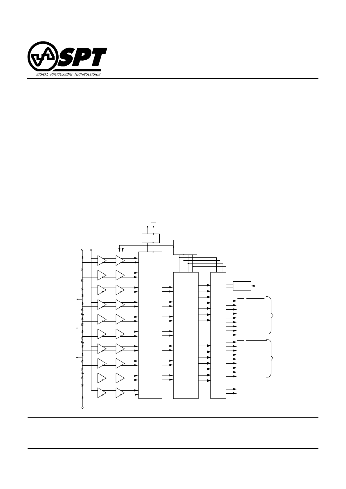
The SPT7610 is a full parallel (flash) analog-to-digital converter capable of digitizing full-scale (0 to –1 V) inputs into
six-bit digital words at an update rate of 1 GSPS. The
ECL-compatible outputs are demultiplexed into two separate output banks, each with differential data-ready outputs to ease the task of data capture. The SPT7610’ s wide
input bandwidth and low capacitance eliminate the need
for external track-and-hold amplifiers for most applications. A proprietary decoding scheme reduces metastable
errors to the 1 LSB level. The SPT7610 operates from a
single –5.2 V supply, with a nominal power dissipation of
2.75 W .
The SPT7610 is available in a 44L hermetic cerquad
surface-mount package in the industrial temperature
range (–40 °C to +85 °C).
64
63
49
48
33
32
17
16
2
1
CLOCK
BUFFER
64 TO 6 BIT DECODER
WITH METASTABLE ERROR CORRECTION
DO
(LSB)
D1
D2
D3
D4
D5
(MSB)
D6
(OVR)
V
RT
Analog
Input
Preamp Comparator
V
RM
V
RB
CLKCLK
DEMUX
CLOCK
BUFFER
1:2 DEMULTIPLEXER
ECL OUTPUT BUFFERS AND LATCHES
DRB (DATA READY)
DRB (DATA READY)
D6B (OVR)
D5B (MSB)
D4B
D3B
D2B
D1B
D0B (LSB)
DRA (DATA READY)
DRA (DATA READY)
D6A (OVR)
D5A (MSB)
D4A
D3A
D2A
D1A
D0A (LSB)
D6B
D5B
D4B
D3B
D2B
D1B
D0B
D6A
D5A
D4A
D3A
D2A
D1A
D0A
BANK B
BANK A
V
R1
V
R3
MINV
LINV
TESTABILITY
TEST
BLOCK DIAGRAM
Page 2

SPT
2 1/30/01
SPT7610
ABSOLUTE MAXIMUM RATINGS (Beyond which damage may occur)1 25 °C
Supply Voltages
Negative Supply Voltage (AVEE TO GND) .–7.0 to +0.5 V
Ground V oltage Differential........................–0.5 to +0.5 V
Input Voltage
Analog Input Voltage ................................+0.5 V to AV
EE
Reference Input Voltage ...........................+0.5 V to AV
EE
Digital Input Voltage.................................. +0.5 V to AV
EE
Reference Current VRT to VRB............................+20 mA
Note: 1. Operation at any Absolute Maximum Rating is not implied. See
Electrical Specifications for proper nominal applied conditions
in typical applications.
Output
Digital Output Current...................................0 to –25 mA
Temperature
Operating Temperature, Ambient............... –40 to +85 °C
Lead Temperature, (soldering 10 seconds) ........ +300 °C
Storage Temperature ............................... –65 to +150 °C
ELECTRICAL SPECIFICATIONS
TA = T
MIN
to T
MAX
, AV
EE
= –5.2 V , V
RB
= –1.00 V , V
RM
= –0.5 V , V
RT
= 0.00 V, ƒ
CLK
= 1000 MSPS, Duty Cycle = 50%, unless otherwise specified.
TEST TEST SPT7610
PARAMETERS CONDITIONS LEVEL MIN TYP MAX UNITS
Resolution 6 Bits
DC Accuracy
Integral Linearity VI –0.5 +0.5 LSB
Differential Linearity VI –0.5 +0.5 LSB
No missing codes VI Guaranteed
Analog Input
Offset Error V
RT
VI –30 +30 mV
Offset Error V
RB
VI –30 +30 mV
Input Voltage Range VI –1 0.0 Volts
Input Capacitance Over Full Input Range V 8 pF
Input Resistance V 50 kΩ
Input Bias Current VI 200 400 µA
Bandwidth Small Signal V 1.4 GHz
Input Slew Rate V 5 V/ns
Clock Synchronous Input Currents V 2 µA
Power Supply Requirements
Supply Current VI 550 770 mA
Power Dissipation VI 2.85 4.0 W
Reference Inputs
Ladder Resistance VI 60 80 120 Ω
Reference Bandwidth V 100 MHz
Digital Outputs
Digital Output High Voltage R
1
= 50 Ω to –2 V VI –1.2 –0.9 Volts
Digital Output Low Voltage R1 = 50 Ω to –2 V VI –1.8 –1.5 Volts
Digital Inputs
Digital Input High Voltage
(CLK, NCLK) VI –1.1 –0.7 Volts
Digital Input Low Voltage
(CLK, NCLK) VI –2.0 –1.5 Volts
Clock Input Swing
(CLK, NCLK) IV 100 700 mV
Maximum Sample Rate VI 1000 1200 MSPS
Clock Low Width, TPW0 VI 0.5 0.4 ns
Clock High Width, TPW1 VI 0.5 0.4 ns
Page 3

SPT
3 1/30/01
SPT7610
ELECTRICAL SPECIFICATIONS
TA = T
MIN
to T
MAX
, AV
EE
= –5.2 V , V
RB
= –1.00 V , V
RM
= –0.5 V , V
RT
= 0.00 V, ƒ
CLK
= 1000 MSPS, Duty Cycle = 50%, unless otherwise specified.
TEST TEST SPT7610
PARAMETERS CONDITIONS LEVEL MIN TYP MAX UNITS
Timing Characteristics
Clock to Data Ready delay (t
dr
) +25 °C case V 950 ps
Clock to Output Data (t
od
) +25 °C case V 1.25 ns
Output Data to Data Ready (t
odr
) –40 to 85 °C case IV 550 750 950 ps
Output Data Skew (t
osk
) –40 to 85 °C case IV –150 150 ps
Aperture Jitter V 2 ps
Acquisition Time V 250 ps
Dynamic Performance
Spurious Free Dynamic Range (SFDR)
ƒ
IN
= 250 MHz V 45 dB
ƒ
IN
= 400 MHz V 34 dB
Signal-to-Noise and Distortion (SINAD)
ƒ
IN
= 250 MHz VI 31 34 dB
ƒ
IN
= 400 MHz VI 28 32 dB
Signal to Noise Ratio (SNR)
ƒ
IN
= 250 MHz VI 33 36 dB
ƒ
IN
= 400 MHz VI 32 36 dB
Total Harmonic Distortion (THD)
ƒ
IN
= 250 MHz VI –40 –37 dB
ƒ
IN
= 400 MHz VI –34 –30 dB
TEST LEVEL CODES
All electrical characteristics are subject to the
following conditions:
All parameters having min/max specifications
are guaranteed. The Test Level column indicates the specific device testing actually performed during production and Quality Assurance inspection. Any b lank section in the data
column indicates that the specification is not
tested at the specified condition.
Unless otherwise noted, all test are pulsed
tests; therefore, T
J
= TC = TA.
LEVEL TEST PROCEDURE
I 100% production tested at the specified temperature.
II 100% production tested at TA = +25 °C, and sample tested at the
specified temperatures.
III QA sample tested only at the specified temperatures.
IV Parameter is guaranteed (but not tested) by design and characteri-
zation data.
V Parameter is a typical value for information pur poses only.
VI 100% production tested at TA = +25 °C. Parameter is guaranteed
over specified temperature range.
Page 4

SPT
4 1/30/01
SPT7610
GENERAL OVER VIEW
The SPT7610 is an ultra high-speed monolithic 6-bit
parallel flash A/D converter. The nominal conversion rate
is 1 GSPS, and the analog bandwidth is typically 1.4 GHz.
A major advance over previous flash converters is the
inclusion of 64 input preamplifiers between the reference
ladder and input comparators. (See the block diagram.)
This not only reduces clock transient kickback to the input
and reference ladder due to a low AC beta but also
reduces the effect of the dynamic state of the input signal
on the latching characteristics of the input comparators.
The preamplifiers act as buffers and stabilize the input
capacitance so that it remains constant over different
input voltage and frequency ranges. This makes the part
easier to drive than previous flash converters. The preamplifiers also add a gain of two to the input signal so that
each comparator has a wider overdrive or threshold range
to “trip” into or out of the active state. This gain reduces
metastable states that can cause errors at the output.
The SPT7610 has true differential analog and digital data
paths from the preamplifiers to the output buffers (Current
Mode Logic) for reducing potential missing codes while
rejecting common mode noise. Signature errors are also
reduced by careful layout of the analog circuitry. The output drive capability of the device can provide full ECL
swings into 50 Ω loads.
Only one –5.2 V power supply is required. Two external
references are applied across the internal reference ladder that has a resistance of 80 Ω typical (60 Ω minimum).
The top reference is typically 0 V or connected to AGND
(analog ground). The device has top force and sense pins
(V
RFT
and V
RST
) that are internally connected together.
These voltage force and sense pins can be used to minimize the voltage drop across the parasitic line resistance.
The bottom reference is typically –1 V . The device also has
bottom force and sense pins (V
RFB
and V
RSB
) that are
internally connected together. These can also be used to
minimize the voltage drop across the parasitic line resistance. Three additional reference taps (V
R3
= –0.25 V typ,
VRM = –0.5 V typ, and VR1 = –0.75 V typ) are brought out.
These taps can be used to control the linearity error.
All logic levels are compatib le with both 10K ECL or 100K
ECL. It is recommended that the clock input be driven
differentially (CLK and NCLK) to improve noise immunity
and reduce aperture jitter.
The digital outputs are split into two banks of 6-bit words
and an overrange bit. Each bank is updated at 1/2 of the
clock rate and is 180° out of phase from the other . The differential data ready signals for each bank are provided to
accurately latch each data bank into the register. The output data is in a straight binary, inverted binary, two’s
complement or inverted two’s complement format. Figure
1 shows a timing diagram of the device and shows the input-to-output relationship, clock-to-output delay and output latency. The SPT7610 has a built-in offset in the ÷2
clock divider (D Flip-Flop) to assure that output bank A will
come up first after power turn on.
Page 5

SPT
5 1/30/01
SPT7610
Figure 1 – Timing Diagram
CLK (1 GHz)
DRA
DRA
Data Bank A
DRB
DRB
Data Bank B
V
IN
N
N+1
N+2
N+3
N+4
1 nsec
t
odB
t
drB
OutputA Skew
(t
oskA
)
DOB-DRB Delay
(t
odrB
)
t
drA
N-4 N
N-2
t
odA
N-1N-3
N-5
OutputB Skew
(t
oskB
)
DOADRA Delay
(t
odrA
)
2
FIRST
RISING EDGE
POWER
ON
8
OUTPUT
BANK A
(DA0-6)
OUTPUT
BANK B
(DB0-6)
DRA
CLK IN
DRB
V
IN
NDRA
NDRB
TEST
3
5
4
2
1
6
INVALID DATA
1
ADC (Normal Operation)
9
10
11
8
TEST MODE
7
t
su
t
dr
t
od
t
dr
t
od
ADC (Normal Operation)
INVALID DATA
INVALID DATA
INVALID DATA
7
9
Bank A Test Pattern 1:
- Even Bits = Hi
- Odd Bits = Low
Bank B Test Pattern 1:
- Even Bits = Hi
- Odd Bits = Low
Bank A Test Pattern 2:
- Even Bits = Low
- Odd Bits = Hi
Bank B Test Pattern 2:
- Even Bits = Low
- Odd Bits = Hi
LOGIC LOW
Figure 2 – Test Mode Timing Diagram
Page 6

SPT
6 1/30/01
SPT7610
TYPICAL INTERFACE CIRCUIT
The typical interface circuit is shown in figure 3. External
reference taps are provided for correcting integral
nonlinearity errors. These taps can be actively driven to
reduce these errors. (See the Reference Inputs discussion below.) The SPT7610 evaluation board application
note contains more details on interfacing the SPT7610.
The function of each pin and external connections to other
components is as follows:
POWER SUPPLY PINS: AVEE, AGND, DGND
AVEE is the supply pin with AGND as ground for the device. The AVEE power supply pin should be bypassed as
close to the device as possible with a 10 µF tantalum capacitor, in parallel with 100 pF and .01 µF chip capacitors.
Place the 100 pF chip capacitor closest to the SPT7610.
Digital ground (DGND) is the ground for the ECL outputs
and is to be referenced to the output pulldown voltage and
appropriately bypassed as shown in figure 3.
ANALOG INPUT: V
IN
There are two analog input pins that are tied to the same
point internally . Either one may be used as an analog input
sense and the other for input force. This is convenient for
testing the source signal to see if there is sufficient drive
capability . The pins can also be tied together and driven by
the same source. The SPT7610 is superior to similar devices due to a preamplifier stage before the comparators.
This makes the device easier to drive because it has constant capacitance and induces less slew rate distortion.
CLOCK INPUTS: CLK, NCLK
The clock inputs are designed to be driven differentially
with ECL levels. The duty cycle of the clock should be kept
at 50% to avoid causing larger second harmonics. If this is
not important to the intended application, then duty cycles
other than 50% may be used.
Figure 3 – Typical Interface Circuit
V
IN
V
IN
V
RTF
V
RTS
*
U1
+
*
U1
+
5.2 V
2N2907
V
RBS
V
RBF
50 W
V
IN
2.0 V
Reference
Convert
2 V
Pulldown
(Analog)
CLK
NCLK
V
RM
R
R
5.2 V
AV
EE
AGND
DGND
*
FB = Ferrite bead
U1 = TLV2464 or equivalent with low offset/noise.
R = 1 kW; 0.05% matched or better
= AGND
= DGND
U2 = Motorola ECLinPS Lite, MC10EL16, differential receiver.
* = 2.2 µF Tantalum Capacitor, 0.1 µF and 100 pF chip capacitors.
** = Care must be taken to avoid exceeding the maximum rating
for the input, especially during power up sequencing of the
analog input driver.
U2
DRB (DATA READY)
DRB (DATA READY)
DRA (DATA READY)
DRA (DATA READY)
DRB
DRA
DRB
DRA
**
FB
*
V
R3
*
V
R1
50 W
D6B (OVR)
D5B (MSB)
D4B
D3B
D2B
D1B
D0B (LSB)
2.0 V
Pulldown
(Digital)
50 W
.1 µF
D6A (OVR)
D5A (MSB)
D4A
D3A
D2A
D1A
D0A (LSB)
Test
LINV
MINV 5.2 V
5.2 V
5.2 V
SPT7610
50 W
5.2 V
22 W
22 W
50 W
Page 7

SPT
7 1/30/01
SPT7610
DIGITAL OUTPUTS: D0 TO D6, DR, NDR (A AND B)
The digital outputs can drive 50 Ω to ECL levels when
pulled down to –2 V. When pulled down to –5.2 V, the outputs can drive 130 Ω to 1 kΩ loads. SPT recommends
using differential receivers on the outputs of the data
ready lines to ensure the proper output rise and fall times.
BINARY AND TWO’S COMPLEMENT OUTPUT:
MINV, LINV
Control pins are provided that enable selection of one of
four digital output formats. (Table I shows selection of
these output formats as a function of the MINV and LINV
pins.) When the MINV pin is high, the MSB output is inverted and when it is low, the it is noninverted. Likewise,
when the LINV pin is high, the LSB output is inverted and
when it is low, the it is noninverted. The user can select
either binary, inverted binary, two’s complement or
inverted two’s complement digital output format.
REFERENCE INPUTS: V
RBF
, V
RBS
, VR1, VRM,
VR3, V
RTF
, V
RTS
There are two reference inputs and three external reference voltage taps. These are –1.0 V V
RBF
(bottom force)
and V
RBS
(bottom sense), –0.75 V VR1 (1/4 tap), –0.5 V
VRM (mid-point tap), –0.25 V VR3 (3/4 tap) and 0.0 V
(AGND) V
RTF
(top force) and V
RTS
(top sense). The top reference pin is normally tied to analog ground (AGND) and
the bottom reference pin can be driven by an op amp as
shown in figure 3.
The reference voltage taps can be used to control integr al
linearity over temperature. The mid-point reference tap
(VRM) is normally driven by an op amp to insure temperature stable operation or may be bypassed for limited temperature operation. The 1/4 (VR1) and 3/4 (VR3) reference
ladder taps are typically bypassed to add noise suppression as shown in figure 3 or may be driven with op amps to
adjust integral linearity .
SPT7610 TEST MODE FUNCTION: TEST PIN
The SPT7610 supports a special test mode function that
overrides the SPT7610’s internal data output latch stage
and exercises the digital outputs in an alternating test pattern. This enables the user to test digital interface logic
downstream from the SPT7610 with a known set of digital
test patterns.
Test mode pin 3 controls the SPT7610 mode of operation
such that when it is low, the SPT7610 operates in normal
mode. When test mode pin 3 is brought high, the
SPT7610 will begin to output test pattern 1 (table II) on the
next rising edge of the clock. (See figure 2.) It will output
the test patterns alternating between test pattern 1 and
test pattern 2 as long as test mode pin 3 is held high. The
minimum set-up time (tsu) can be as low as 0 nsec.
Only the digital output stage is involved in the test mode
operation. All ADC stages before the digital output stage
continue normal data conversion operation while the test
mode is active. When test mode pin 3 is brought bac k low,
the SPT7610 will resume output of valid data on the next
rising edge of the clock. The valid data output will correspond to a two-clock-cycle pipeline delay as shown in
figure 2.
Table II – SPT7610 Test Mode Output Bit Patterns
D6 D5 D4 D3 D2 D1 D0
Test Pattern 1 1010101
Test Pattern 2 0101010
BINARY TWOs COMPLEMENT
TRUE INVERTED TRUE INVERTED
MINV=LINV=0 MINV=LINV=1 MINV=1; LINV=0 MINV=0; LINV=1
ANALOG INPUT VOLTAGE D6 D5_______D
0
D5______D
0
D5______D
0
D5______D
0
–1 V + 1/2 LSB 0 000000 111111 1000000 0111111
0 000001 111110 1000001 0111110
–0.5 V 0 0111111 100000 111111 000000
100000 011111 000000 111111
0 V – 1/2 LSB 0 111111 000000 011111 100000
1 111111 000000 011111 100000
0 V 1 111111 000000 011111 100000
1
Tie MINV/LINV to GND for logic 1.
2
Float MINV/LINV for logic 0. (MINV/LINV are internally pulled down to –5.2 V.)
Ta b le I – Output Coding Table
Page 8

SPT
8 1/30/01
SPT7610
SUBCIRCUIT SCHEMATICS
Figure 3A – Input Circuit Figure 3B – Output Circuit Figure 3C – Clock Input
Data Out
AGND DGND
AGND
AV
EE
V
IN
V
r
AGND
AV
EE
CLK CLK
THERMAL MANAGEMENT
Adequate heat sinking and air flow must be provided to
keep the die temperature below +150 °C. This device is
packaged with the cavity up (the die is on the bottom of
the package). Therefore, SPT recommends that the
device be heat sinked by contacting the bottom of the
package through a hole in the circuit board.
The thermal coefficients of the SPT7610 (44L cerquad)
are as follows:
θja = +78 °C/W (junction to ambient in
still air with no heat sink)
θjc = +4 °C/W (junction to case)
Page 9

SPT
9 1/30/01
SPT7610
PACKAGE OUTLINE
44-Lead Cerquad
INCHESINCHES
INCHESINCHES
INCHES
MILLIMETERSMILLIMETERS
MILLIMETERSMILLIMETERS
MILLIMETERS
SYMBOLSYMBOL
SYMBOLSYMBOL
SYMBOL
MINMIN
MINMIN
MIN
MAXMAX
MAXMAX
MAX
MINMIN
MINMIN
MIN
MAXMAX
MAXMAX
MAX
A 0.551 typ 14.0 typ
B 0.685 0.709 17.40 18.00
C 0.037 0.041 0.94 1.04
D 0.016 typ 0.41 typ
E 0.008 typ 0.20 typ
F 0.027 0.051 0.69 1.30
G 0.006 typ 0.15 typ
H 0.080 0.150 2.03 3.81
C
D
A
B
A
B
05°
E
F
G
H
Page 10

SPT
10 1/30/01
SPT7610
ORDERING INFORMATION
PART NUMBER TEMPERATURE RANGE PACKAGE
SPT7610SIQ –40 to +85 °C 44L Cerquad
Signal Processing Technologies, Inc. reserves the right to change products and specifications without notice. Permission is hereby
expressly granted to copy this literature for informational purposes only. Copying this material for any other use is strictly prohibited.
WARNING – LIFE SUPPORT APPLICATIONS POLICY – SPT products should not be used within Life Support Systems without
the specific written consent of SPT. A Life Support System is a product or system intended to support or sustain life which, if it fails,
can be reasonably expected to result in significant personal injury or death.
Signal Processing Technologies believes that ultrasonic cleaning of its products may damage the wire bonding, leading to device
failure. It is therefore not recommended, and exposure of a device to such a process will void the product warranty.
PIN ASSIGNMENTS PIN FUNCTIONS
Name Function
AV
EE
Negative Supply; nominally –5.2 V
AGND Analog Ground
V
RTF
Reference Voltage Force Top; nominally 0 V
V
RTS
Reference Voltage Sense Top
V
RM
Reference Voltage Middle; nominally –0.5 V
V
RBF
Reference Voltage Force Bottom; nominally –1.0 V
V
RBS
Reference Voltage Sense Bottom
V
IN
Analog Input Voltage; can be either Voltage or
Sense
DGND Digital Ground
D0–D5A Data Output Bank A
D0–D5B Data Output Bank B
DRA Data Ready Bank A
NDRA Not Data Ready Bank A
DRB Data Ready Bank B
NDRB Not Data Ready Bank B
D6A Overrange Output Bank A
D6B Overrange Output Bank B
CLK Clock Input
NCLK Clock Input
MINV MSB Control Pin
LINV LSB Control Pin
TEST Test Control Pin
V
R1
Reference Voltage 1/4, nominally –0.75 V
V
R3
Reference Voltage 3/4, nominally –0.25 V
V
RTF
AV
EE
V
R3
AGND
V
INVIN
AGND
V
RM
V
R1
AV
EE
V
RBF
DGND
D2B
D3B
D4B
D5B
D6B
DGND
DRA
NDRA
D0A
D1A
SPT7610
Top View
44
1
V
RBS
MINV
Test
AGND
AV
EE
D6A
D5A
D4A
D3A
DGND
D2A
V
RTS
AGND
CLK
NCLK
AGND
LINV
AV
EE
DRB
NDRB
D0B
D1B
43
42
41
40
39
383736
35
34
33
32
31
30
29
28
27
26
25
24
23
12 13 14 15 161718 19 20 21 22
2
3
4
5
6
7
8
9
10
11
 Loading...