

Page 1
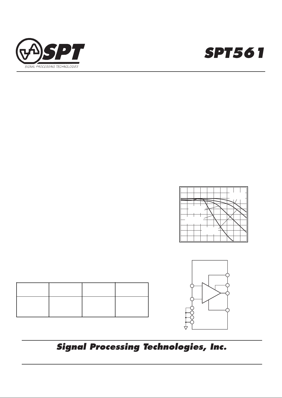
Typical Distortion Performance
Output 20MHz 50MHz 100MHz
Power 2nd 3rd 2nd 3rd 2nd 3rd
10dBm -59 -62 -52 -60 -35 -49
18dBm -52 -48 -45 -46 -30 -36
24dBm -50 -41 -36 -32 -40 -30
Frequency Response vs. Output Power
Gain (dB)
Frequency (MHz)
16
12
6
0 40 80 120 160 200
10
8
14
Po = 10dBm
V
o
= 2V
pp
Po = 24dBm
V
o
= 10V
pp
Po = 27.5dBm
V
o
= 15V
pp
Po = 18dBm
V
o
= 5V
pp
Features
■
150MHz bandwidth at +24dBm output
■
Low distortion (2nd/3rd:
-59/-62dBc @ 20MHz and 10dBm)
■
Output short circuit protection
■
User-definable output impedance, gain,
and compensation
■
Internal current limiting
■
Direct replacement for CLC561
Applications
■
Output amplification
■
Arbitrary waveform generation
■
ATE systems
■
Cable/line driving
■
Function generators
■
SAW drivers
■
Flash A/D driving and testing
4755 Forge Road, Colorado Springs, Colorado 80907, USA
Phone: (719) 528-2300 FAX: (719) 528-2370 Website: http://www.spt.com E-Mail: sales@spt.com
WIDEBAND, LOW DISTORTION DRIVER AMPLIFIER
General Description
The SPT561 is a wideband DC coupled, amplifier that combines high
output drive and low distortion. At an output of +24dBm (10Vpp into
50Ω), the -3dB bandwidth is 150MHz. As illustrated in the table
below, distortion performance remains excellent even when amplifying high-frequency signals to high output power levels.
With the output current internally limited to 250mA, the SPT561 is
fully protected against shorts to ground and can, with the addition of a
series limiting resistor at the output, withstand shorts to the ±15V
supplies.
The SPT561 has been designed for maximum flexibility in a wide
variety of demanding applications. The two resistors comprising the
feedback network set both the gain and the output impedance,
without requiring the series backmatch resistor needed by most op
amps. This allows driving into a matched load without dropping half
the voltage swing through a series matching resistor. External
compensation allows user adjustment of the frequency response.
The SPT561 is specified for both maximally flat frequency response
and 0% pulse overshoot compensations.
The combination of wide bandwidth, high output power, and low
distortion, coupled with gain, output impedance and frequency
response flexibility, makes the SPT561 ideal for waveform generator
applications. Excellent stability driving capacitive loads yields superior performance driving ADC’s, long transmission lines, and SAW
devices.
The SPT561 is constructed using thin film resistor/bipolar transistor
technology, and is available in the following versions:
SPT561AIJ -25°C to +85°C 24-pin Ceramic DIP
SPT561AMJ -55°C to +125°C 24-pin Ceramic DIP, features
burn-in and hermetic testing
4
19
23
21
20
15
10
5
18
8
+
-
Compensation
V
o
-V
CC
All undesignated
pins are internally
unconnected. May
be grounded if
desired.
+V
CC
V+
V-
Block Diagram
Page 2

2 10/9/98
SPT561
PARAMETERS CONDITIONS TYP MIN & MAX RATINGS UNITS SYM
Case Temperature SPT561AIJ +25°C -25°C +25°C +85°C
Case Temperature SPT561AMJ +25°C -55°C +25°C +125°C
FREQUENCY DOMAIN RESPONSE (Max. Flat Compensation)
✝ -3dB bandwidth
✝ maximally flat compensation V
o
<2Vpp (+10dBm) 215 >175 >185 >175 MHz SSBW
0% overshoot compensation V
o
<2Vpp (+10dBm) 210 >170 >180 >170 MHz
large signal bandwidth Vo <10Vpp (+24dBm) 150 >145 >135 >120 MHz FPBW
(see Frequency Response vs. Output Power plot)
gain flatness Vo <2Vpp (+10dBm)
✝ peaking 0.1 -50MHz 0 <0.50 <0.40 <0.50 dB GFPL
✝ peaking >50MHz 0 <1.75 <0.75 <1.00 dB GFPH
✝ rolloff at 100MHz 0.1 <1.00 <0.75 <1.00 dB GFR
group delay to 100MHz 2.9 – – – ns GD
linear phase deviation to 100MHz 0.6 <1.7 <1.2 <1.7 ° LPD
return loss (
see discussion of R
x
) to 100MHz -15 <-11 <-11 <-11 dB RL
DISTORTION (Max. Flat Compensation)
2nd harmonic distortion
✝ 24dBm (10V
pp
): 20MHz -50 <-38 <-40 <-38 dBc HD2HL
✝ 50MHz -36 <-29 <-29 <-22 dBc HD2HM
100MHz -40 <-25 <-25 <-25 dBc HD2HH
✝ 18dBm (5V
pp
): 20MHz -52 <-42 <-44 <-42 dBc HD2ML
✝ 50MHz -45 <-30 <-35 <-30 dBc HD2MM
✝ 100MHz -30 <-22 <-25 <-25 dBc HD2MH
✝ 10dBm (2V
pp
): 20MHz -59 <-48 <-52 <-48 dBc HD2LL
✝ 50MHz -52 <-36 <-40 <-40 dBc HD2LM
100MHz -35 <-27 <-28 <-28 dBc HD2LH
3rd harmonic distortion
✝ 24dBm (10V
pp
): 20MHz -41 <-34 <-34 <-30 dBc HD3HL
✝ 50MHz -32 <-26 <-26 <-21 dBc HD3HM
✝ 100MHz -30 <-24 <-24 <-24 dBc HD3HH
✝ 18dBm (5V
pp
): 20MHz -48 <-40 <-44 <-44 dBc HD3ML
✝ 50MHz -46 <-37 <-37 <-35 dBc HD3MM
100MHz -36 <-30 <-30 <-30 dBc HD3MH
✝ 10dBm (2V
pp
): 20MHz -62 <-54 <-57 <-57 dBc HD3LL
✝ 50MHz -60 <-49 <-52 <-49 dBc HD3LM
100MHz -49 <-45 <-45 <-45 dBc HD3LH
2-tone 3rd order
intermod intercept
2
20MHz 38 >36 >36 >36 dBm IM3L
50MHz 35 >32 >32 >32 dBm IM3M
100MHZ 29 >27 >27 >23 dBm IM3H
Min/max ratings are based on product characterization and simulation. Individual parameters are tested as noted. Outgoing quality levels are
determined from tested parameters.
SPT561 Electrical Characteristics
(Av = +10V, VCC = ±15V, RL = 50Ω, Rf = 410Ω, Rg = 40Ω, Ro = 50Ω; unless specified)
NOTES TO THE ELECTRICAL SPECIFICATIONS
The electrical characteristics shown here apply to the specific test conditions shown above (see also Figure 1 in
description of the operation). The SPT561 provides an equivalent, non-zero, output impedance determined by the
external resistors. The signal gain to the load is therefore load dependent. The signal gain shown above (Av = +10)
is the no load gain. The actual gain to the matching 50Ω load used in these specifications is half of this (+5).
The SPT561 requires an external compensation capacitor. Unless otherwise noted, this has been set to 10.5pF for
the frequency domain specifications (yielding a maximally flat frequency response) and 12.5pF for the time domain
specifications (yielding a 0% small signal pulse overshoot response).
Page 3

3 10/9/98
SPT561
PARAMETERS CONDITIONS TYP MIN & MAX RATINGS UNITS SYM
Case Temperature SPT561AIJ +25°C -25°C +25°C +85°C
Case Temperature SPT561AMJ +25°C -55°C +25°C +125°C
TIME DOMAIN RESPONSE (0% Overshoot Compensation)
rise and fall time
2V step 1.5 <2.0 <1.9 <2.0 ns TRS
10V step 2.4 <2.8 <2.8 <3.4 ns TRL
settling time to 0.5% (time <1µs) 5V step 7 <12 <12 <15 ns TS
long term thermal tail (time >1µs) 5V step 1.5 <2.0 <2.0 <2.0 % SE
slew rate 10V
pp
, 175MHz 3300 >3000 >2900 >2500 V/µsSR
overshoot 2V step
maximally flat compensation 5 <13 <10 <13 % OSMF
0% overshoot compensation 0 <5 <3 <5 % OSZO
EQUIVALENT INPUT NOISE
voltage >100KHz 2.1 <2.5 <2.5 <2.5 nV/√Hz VN
inverting current >100KHz 34 <40 <40 <45 pA/√Hz ICN
non-inverting current >100KHz 2.8 <4.5 <4.5 <5.0 pA/√Hz NCN
noise floor >100KHz -159 <-157 <-157 <-157
dBm/(1Hz) SNF
integrated noise 1kHz to 200MHz 35 <45 <45 <45 µV INV
noise figure >100KHz 15 <17 <17 <17 dB NF
STATIC, DC PERFORMANCE
* input offset voltage 2.0 <14.0 <5.0 <15.0 mV VIO
average temperature coefficient 35 <100 – <100 µV/°C DVIO
* non-inverting bias current 5.0 <35 <20 <20 µA IBN
average temperature coefficient 20 <175 – <100 nA/°C DIBN
* inverting bias current 10.0 <50 <30 <50 µA IBI
average temperature coefficient 100 <200 – <200 nA/°C DIBI
* power supply rejection ratio (DC) 57 >54 >54 >52 dB PSRR
* supply current no load 50 <60 <60 <65 mA ICC
MISCELLANEOUS PERFORMANCE
open loop current gain (±2% tolerance) 10.0 – – – mA/mA G
average temperature coefficient +0.02 <+.03 – <+.02 %/°CDG
inverting input resistance (±5% tolerance) 14.0 – – – Ω RIN
average temperature coefficient +.02 <+.025 – <+.025 Ω/°C DRIN
non-inverting input resistance 700 >200 >400 >400 KΩ RNI
non-inverting input capacitance to 100MHz 2.7 <3.5 <3.5 <3.5 pF CNI
output voltage range 150mA load current ±10.5 – >±10.0 – V VO
output current limit 210 <250 <250 <250 mA OCL
Min/max ratings are based on product characterization and simulation. Individual parameters are tested as noted. Outgoing quality levels are
determined from tested parameters.
Absolute Maximum Ratings Recommended Operating Conditions
V
CC
(reversed supplies will destroy part) ±20V V
CC
±10V to ±15V
differential input voltage ±3V I
o
≤ ±200mA
common mode input voltage ±V
CC
common mode input voltage < ±(|VCC| -6)V
junction temperature (see thermal model) +175°C output impedance 25Ω to 200Ω
storage temperature -65°C to +150°C gain range (no-load voltage gain) +5 to +80
lead temperature (soldering 10s) +300°C case temperature: AIJ -25°C to +85°C
output current (internally limited) ±250mA AMJ -55°C to +125°C
Notes
1) * AIJ, AMJ 100% tested at +25°C
✝ AMJ 100% tested at at +25°C and sample tested
at -55°C and +125°C
✝ AIJ sample tested at +25°C
2) Test Tones are set ±100kHz of indicated frequency.
SPT561 Electrical Characteristics
(Av = +10V, VCC = ±15V, RL = 50Ω, Rf = 410Ω, Rg = 40Ω, Ro = 50Ω; unless specified)
Page 4
4 10/9/98
SPT561
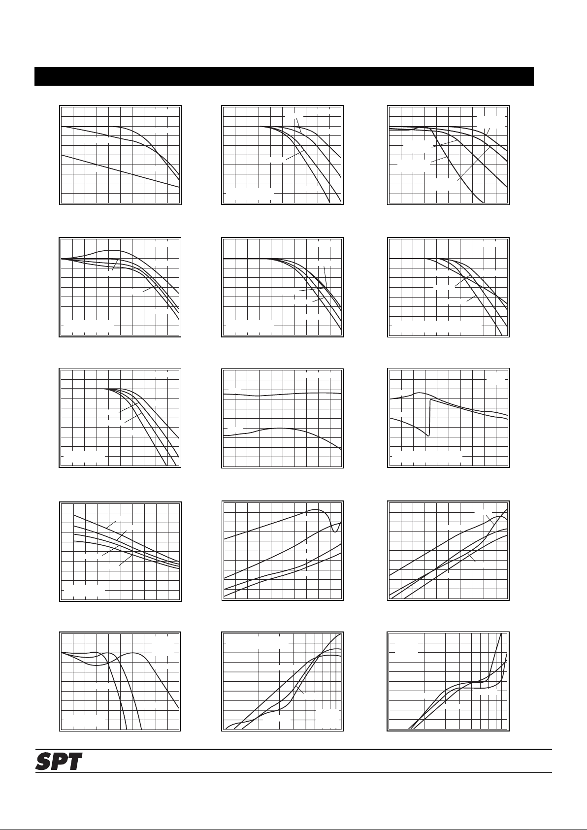
Small Signal Gain and Phase
Gain (dB)
Frequency (MHz)
6
8
10
12
14
16
0 50 100 150 200 250
Maximally Flat
Phase (degrees)
0
-90
-360
-180
-270
0% Overshoot
Gain
Phase
Po = 10dBm
Frequency Response vs. Gain
Normalized Magnitude (1dB/div)
Frequency (MHz)
0 50 100 150 200 250
Po = 10dBm
Av = 10
Av = 5
Av = 15
Av = 20
Re-compensated at
each gain (see text)
Frequency Response vs. Output Power
Gain (dB)
Frequency (MHz)
16
12
6
0 40 80 120 160 200
10
8
14
Po = 10dBm
V
o
= 2V
pp
Po = 24dBm
V
o
= 10V
pp
Po = 27.5dBm
V
o
= 15V
pp
Po = 18dBm
V
o
= 5V
pp
Frequency Response vs. R
L
Normalized Magnitude (1dB/div)
Frequency (MHz)
0 50 100 150 200 250
Pi = -4dBm
RL = 50Ω
RL = 25Ω
RL = 75Ω
RL = 100Ω
Fixed gain and
compensated vs. load
Frequency Response vs. Power Supply
Frequency (MHz)
0 50 100 150 200 250
Po = 10dBm
±VCC = 18
±VCC = 12
±VCC = 15
±VCC = 10
Gain (dB)
16
12
6
10
8
14
Re-compensated at
each supply voltage
Frequency Response vs. R
o
Frequency (MHz)
0 50 100 150 200 250
Pi = -4dBm
Normalized Magnitude (1dB/div)
Ro = 50Ω
Ro = 25Ω
Ro = 75Ω
Ro = 100Ω
Response measured with matched load
Re-compensated at each R
o
Frequency Response vs. Gain (R
o, RL
= 75Ω)
Frequency (MHz)
0 50 100 150 200 250
Vo = 2V
pp
Normalized Magnitude (1dB/div)
Av = 5
Av = 10
Av = 15
Av = 20
Re-compensated
at each gain
Gain Flatness/Deviation from Linear Phase
Gain (0.1dB/div)
Frequency (MHz)
0 20406080100
Phase (0.5°/div)
Gain
Phase
Po = 10dBm
Internal Current Gain and Phase
Gain (10dB/div)
Frequency (MHz)
-30
-20
0
20
30
10
0 100 200 300 400 500
Phase (90°/div)
180
90
-180
0
-90
Gain
Phase
-10
Cx = 0
R
L
= 0
Phase consistant with current
polarity connection of Figure 3
Two Tone, 3rd-Order Intermodulation
Intercept (2.5dB/div)
Frequency (MHz)
45
35
20
0 20406080100
30
25
40
Av = 15
Av = 5
Av = 10
Av = 20
Re-compensated
at each gain
2nd Harmonic Distortion vs. Frequency
Distortion (dBc)
Output Power (dB)
-25
-45
-75
4 8 12 16 20 24
-55
-65
-35
50MHz
10MHz
20MHz
100MHz
3rd Harmonic Distortion vs. Frequency
Distortion (dBc)
Output Power (dB)
-25
-45
-75
4 8 12 16 20 24
-55
-65
-35
50MHz
10MHz
20MHz
100MHz
Frequency Response Driving C
L
Frequency (MHz)
0 50 100 150 200 250
Gain (1dB/div)
Av = +5
R
o
= 25
V
o
= 2V
pp
CL = 100pF
CL = 20pF
CL = 50pF
Re-compensated
at each C
L
2nd Harmonic Distortion Driving C
L
Frequency (MHz)
10 20 30 40 50 100
Distortion (5dBc/div)
Av = +5
R
o
= 25
V
o
= 2V
pp
CL = 100pF
CL = 20pF
CL = 50pF
70
-80
-70
-60
-50
-40
-30
Compensation as shown in
Frequency Response plot
3rd Harmonic Distortion Driving C
L
Frequency (MHz)
10 20 30 40 50 100
Distortion (5dBc/div)
Av = +5
R
o
= 25
V
o
= 2V
pp
CL = 100pF
CL = 20pF
CL = 50pF
70
-80
-70
-60
-50
-40
-30
SPT561 Typical Performance Characteristics
(TA = +25°C, Circuit in Figure 1; unless specified)
Page 5

5 10/9/98
SPT561
Small Signal Pulse Response
Time (2ns/div)
Output Voltage (V)
Maximally Flat
Compensation
0
-1.2
-0.8
-0.4
0.4
1.2
0% Overshoot
Compensation
0.8
Large Signal Pulse Response
Time (5ns/div)
Output Voltage (V)
Maximally Flat
Compensation
0
-6
-4
-2
2
6
0% Overshoot
Compensation
4
Uni-Polar Pulse Response
Time (5ns/div)
Output Voltage (V)
Maximally Flat
Compensation
0
-6
-4
-2
2
6
4
Settling Time into 50Ω Load
Time (sec)
Settling Error (%)
0
-1.5
-1.0
-0.5
0.5
1.5
1.0
2.0
-2.0
10
-9
10-710-510-310-110
1
5V Output Step
Settling Time into 500Ω Load
Time (sec)
Settling Error (%)
5V Output Step
0
-1.5
-1.0
-0.5
0.5
1.5
1.0
2.0
-2.0
10
-9
10-710-510-310-110
1
Reverse Transmission Gain & Phase (S12)
Reverse Gain (dB)
Frequency (MHz)
-100
-80
-60
-40
-20
0
0 50 100 150 200 250
Reverse Phase (degrees)
0
-45
-180
-90
-135
Gain
Phase
Settling Time into 50pF Load
Time (sec)
Settling Error (%)
5V Output Step
0
-1.5
-1.0
-0.5
0.5
1.5
1.0
2.0
-2.0
10
-9
10-710-510-310-110
1
Output Return Loss (S22)
Magnitude (dB)
Frequency (MHz)
-25
-20
-15
-10
-5
0
0 50 100 150 200 250
Ro = 50Ω
R
x
= 0Ω
-50
-45
-40
-35
-30
Ro = 40Ω
R
x
= 10Ω
Re-compensated
at each R
x
Input Return Loss (S11)
Magnitude (dB)
Frequency (MHz)
-50
-40
-30
-20
-10
0
0 50 100 150 200 250
Phase (degrees)
0
-45
-180
-90
-135
Magnitude
Phase
Re-compensated
at each R
x
-1dB Compensation Point
-1dB Compensation (dBm)
Frequency (MHz)
29
30
31
32
33
34
0 20406080100
Ro = 50Ω
24
25
26
27
28
Ro = 75Ω
Match Load
Re-compensated at each load
Noise Figure
Noise Figure (dBm)
No Load Gain
17
18
19
20
21
22
5 1015202530
Ro = 50Ω
12
13
14
15
16
Ro = 25Ω
Ro = 75Ω
Ro = 100Ω
Non-inverting input impedance
matched to source impedance
Equivalent Input Noise
Noise Voltage (nV/√Hz)
Frequency (Hz)
1
6
20
40
60
100
100 1k 10k 100k 10M 100M
Inverting Current 34pA/√Hz
Noise Current (pA/√Hz)
10
4
2
1
6
20
40
60
100
10
4
2
Non-Inverting Voltage 2.1nV/√Hz
Non-Inverting Current 2.8pA/√Hz
1M
Group Delay
Group Delay (ns)
Frequency (MHz)
3.0
3.2
3.4
3.6
3.8
4.0
0 50 100 150 200 250
2.0
2.2
2.4
2.6
2.8
Aperture set to 5%
of span (12.8MHz)
Gain Error Band (Worst Case, DC)
Gain Error at Load (%)
No Load Gain
0
1
2
3
4
5
5 9 13 17 21 25
-5
-4
-3
-2
-1
Ro (nominal) = 50Ω
R
L
= 50Ω ± 0%
Rf and R
g
tolerance = ±0.1%
Rf and R
g
tolerance = ±1%
PSRR
PSRR (dB)
Frequency (Hz)
50
60
70
80
90
100
100 1k 10k 100k 1M 100M
0
10
20
30
40
10M
SPT561 Typical Performance Characteristics
(TA = +25°C, Circuit in Figure 1; unless specified)
Page 6

6 10/9/98
SPT561
Rf – Feedback resistor
from output to inverting
input
Rg – Gain setting
resistor from inverting
input to ground
Cx – External
compensation capacitor
from output to
pin 19 (in pF)
Where:
Ro – Desired equivalent output impedance
Av– Non-inverting input to output voltage
gain with no load
G – Internal current gain from inverting input
to output = 10 ±1%
Ri– Internal inverting input impedance = 14Ω ±%5
Rs– Non-inverting input termination resistor
RL– Load resistor
AL– Voltage gain from non-inverting input to
load resistor
RG1RAR
R
RR
A1
C
1
R
300 1
2
R
0.08
f
ovi
g
f
o
v
x
o
g
=+
()
−
=
−
−
=
−
−
SUMMARY DESIGN EQUATIONS AND DEFINITIONS
SPT561 Description of Operation
Looking at the circuit of Figure 1 (the topology and
resistor values used in setting the data sheet specifications), the SPT561 appears to bear a strong external
resemblance to a classical op amp. As shown in the
simplified block diagram of Figure 2, however, it differs in
several key areas. Principally, the error signal is a
current into the inverting input (current feedback) and the
forward gain from this current to the output is relatively
low, but very well controlled, current gain. The SPT561
has been intentionally designed to have a low internal
gain and a current mode output in order that an equivalent
output impedance can be achieved without the series
matching resistor more commonly required of low output
impedance op amps. Many of the benefits of a high loop
gain have, however, been retained through a very careful
control of the SPT561’s internal characteristics.
The feedback and gain setting resistors determine both
the output impedance and the gain. Rf predominately
sets the output impedance (Ro), while Rg predominately
determines the no load gain (Av). solving for the required
Rf and Rg, given a desired Ro and Av, yields the design
equations shown below. Conversely, given an Rf and Rg,
the performance equations show that both Rf and Rg play
a part in setting Ro and Av. Independent Ro and A
v
adjustment would be possible if the inverting input impedance (Ri) were 0 but, with Ri = 14Ω as shown in the
specification listing, independent gain and output impedance setting is not directly possible.
Figure 1: Test Circuit
Design Equations
RG1RAR
R
RR
A1
f
ovi
g
f
o
v
=+
()
−
=
−
−
R
RR1
R
R
G1
R
R
A1
R
R
G
R
R
G1
R
R
o
f
i
f
g
i
g
v
f
g
i
f
i
g
=
++
++
=+
−
++
Simplified Circuit Description
Looking at the SPT561’s simplified schematic in Figure 2, the
amplifier’s operation may be described. Going from the noninverting input at pin 8 to the inverting input at pin 18,
transistors Q1 – Q4 act as an open loop unity gain buffer
forcing the inverting node voltage to follow the non-inverting
voltage input.
Transistors Q3 and Q4 also act as a low impedance (14Ω
looking into pin 18) path for the feedback error current. This
current, (i
err
), flows through those transistors into a very well
defined current mirror having a gain of 10 from this error
current to the output. The current mirror outputs act as the
amplifier output.
The input stage bias currents are supply voltage independent.
Since these set the bias level for the whole part, relatively
constant performance over supply voltage is achieved. A
current sense in the error current leg of the 10X current mirror
Where:
G ≡ forward current gain
(=10)
Ri≡ inverting node input
resistance (=14Ω)
Ro ≡ desired output
impedance
Av≡ desired non-
inverting voltage
gain with no load
Performance Equations
6.8µF.1µF
-V
CC
(-15)
410Ω
R
g
40Ω
5,10,15,
20
R
f
21
SPT561
+
-
18
R
s
50Ω
8
V
i
(Pi)
R
L
50Ω
V
o
(Po)
R
o
4
19
+V
CC
(+15)
.1µF
6.8µF
+
+
C
x
23
10.5pF
Resistor Values
shown result in:
Ro = 50Ω
Av = +10
(no-load gain)
A
L
= +5 [14dB]
(gain to 50Ω load)
Page 7

7 10/9/98
SPT561
R
g
R
o
i
err
V
o
R
f
C
x
19
I
o
I
o
I
bias
10X Current Mirror
Current Limit
5pF
Q3
Q1
-V
CC
+V
CC
4
I
bias
10X Current Mirror
Current Limit
5pF
Q4
Q2
+V
CC
-V
CC
21
23
8
V
i
i
err
R
g
R
f
i
f
Gi
err
R
o
V
o
X1
R
i
l
o
V
-
+
-
V i R and
ii
V
R
i1
R
R
VViRi RR1
R
R
ViRR1
R
R
and
IGi iiG1
err i
f
err
g
err
i
g
o
ff
err i
f
i
g
o err
f
i
f
g
o err
f
err
−
−
−
=
=+ = +
=+ = + +
=++
=+= +
++
≡=
++
++
=
+
=
R
R
then
R
V
I
RR1
R
R
G1
R
R
note that R
R
G1
R0
i
g
o
o
o
f
i
f
g
i
g
o
f
i
i
err
R
g
R
f
Gi
err
V
o
X1
R
i
V
-
+
-
V
i
Noload gain
A
V
V
v
o
i
≡
feeds back to the bias current setup providing a current
shutdown feature when the output current approaches
250mA.
Figure 2: Simplified Circuit Diagram
Developing the Performance Equations
The SPT561 is intended to provide both a controllable
voltage gain from input to output as well as a controllable
output impedance. It is best to treat these two operations
separately with no load in place. Then, with the no-load
gain and output impedance determined, the gain to the
load will simply be the no-load gain attenuated by the
voltage divider formed by the load and the equivalent
output impedance.
Figure 3 steps through the output impedance development using an equivalent model of Figure 2. Offering an
equivalent, non-zero, output impedance into a matched
load allows the SPT561 to operate at lower internal
voltage swings for a given desired swing at the load. This
allows higher voltage swings to be delivered at the load
for a given power supply voltage at lower distortion levels
than an equivalent op amp needing to generate twice the
voltage swing actually desired at the matched load. This
improved distortion is specified and tested over a wide
range as shown in the specification listing.
Get both Vo and Io into terms of just the error current, i
err
,
using:
Figure 3: Output Impedance Derivation
Note that the Ro expression simplifies considerably if
Ri = 0. Also note that if the forward current gain were to go
to infinity , the output impedance would go to 0. This would
be the normal op amp topology with a very high internal
gain. The SPT561 achieves a non-zero Ro by
setting the internal forward gain to be a low, well
controlled, value .
Developing the No-Load Gain Expression
Taking the output impedance expression as one constraint setting the external resistor values, we now need
to develop the no-load voltage gain expression from the
non-inverting input to the output as the other constraint.
Figure 4 shows the derivation of the no load gain.
Page 8

8 10/9/98
SPT561
recognize that [takingV positive]
V V Gi R
solvingfor V from two directions
V ViR G1iR
solvingfor i fromthis
i
V
G1R R
then
VV
VR
G1R R
and,substitutingfor V and i in the original V expression
VV1
GR R
i
o err
f
i err i err g
err
err
i
gi
i
ii
gi
err o
oi
f
=+
=− = +
()
=
+
()
+
=−
+
()
+
=+
−
−
−
−
−
−
ii
gi
f
g
v
o
i
f
g
i
f
i
g
v
f
g
i
G1R R
pullingan
R
R
out of the fraction
A
V
V
1
R
R
G
R
R
G1
R
R
note that A 1
R
RGG1
R0
+
()
+
≡=+
−
++
=+
+
=
R
RR
R
R
G
R
R
A
R
R
G
R
R
G
R
R
o
f
i
f
g
i
g
v
f
g
i
f
i
g
=
++
++
=+
−
++
1
1
1
1
RGRAR
R
RR
A
f
ovi
g
f
o
v
=+
()
−
=
−
−11
Figure 4: Voltage Gain Derivation
Note again that if Ri = 0 this expression would simplify
considerably. Also, if G were very large the voltage gain
expression would reduce to the familiar non-inverting op
amp gain equation. These two performance equations,
shown below, provide a means to derive the design
equations for Rf and Rg given a desired no load gain and
output impedance. The details of that derivation may be
found in Application Note SPT-01.
Performance Equations Design Equations
Equivalent Model
Given that the physical feedback and gain setting
resistors have been determined in accordance with the
design equations shown above, an equivalent model may
be created for the gain to the load where the amplifier block
is taken as a standard op amp. Figure 5 shows this analysis
model and the resulting gain equation to the load.
R
g
V
i
R
L
V
o
R
o
Rf - R
o
Classical
op-amp
+
-
V
V
1
RR
R
R
RR
substitutinginfor R andR withtheir design
equationyields
V
V
A
R
RR
A (gain to load)
o
i
f
o
g
L
Lo
f
g
o
i
v
L
Lo
L
=+
−
+
=
+
=
Figure 5: Equivalent Model
This model is used to generate the DC error and noise
performance equations. As with any equivalent model, the
primary intent is to match the external terminal characteristics recognizing that the model distorts the internal currents
and voltages. In this case, the model would incorrectly
predict the output pin voltage swing for a given swing at the
load. But it does provide a simplified means of getting to the
external terminal characteristics.
External Compensation Capacitor (Cx)
As shown in the test circuit of Figure 1, the SPT561 requires
an external compensation capacitor from the output to pin
19. The recommended values described here assume that a
maximally flat frequency response into a matched load is
desired. The required Cx varies widely with the desired value
of output impedance and to a lesser degree on the desired
gain. Note from Figure 2, the simplified internal schematic,
that the actual total compensation (Ct) is the series combination of Cx and the internal 10pF from pin 19 to the
compensation nodes. With this total value derived, the
required external Cx is developed by backing out the effect
of the internal 10pF. The total compensation (Ct) is developed in two steps as shown below.
C
300
R
1
2.0
R
pFintermediate equation
C
C
1 0.02 C
pF totalcompensation
1
og
t
1
1
=−
=
+
()
Page 9

9 10/9/98
SPT561
This, and an expression for the external Cx without the
intermediate steps are shown below.
C
10C
10 C
or
C
1
R
300 1
2
R
0.08
pF
x
t
t
x
o
g
=
−
=
−
−
The plot in Figure 6 shows the required Cx vs. gain for
several desired output impedances using the equations
shown above. Note that for lower Ro’s, Cx can get very
large. But, since the total compensation is actually the
series combination of Cx and 10pF, going to very high
Cx’s is increasingly ineffective as the total compensation
is only slightly changed. This, in part, sets the lower limits
on allowable Ro.
C
x
(pF)
No Load Voltage Gain
0
2
4
6
8
10
12
14
16
18
20
5
10 15 20 25
30
35 40 45 50 55
Maximally Flat Response
into a Matched Load
Ro = 50Ω
Ro = 75Ω
Ro = 100Ω
Figure 6: External Compensation Capacitance (Cx)
A 0% small signal overshoot response can be achieved
by increasing Cx slightly from the maximally flat value.
Note that this applies only for small signals due to slew
rate effects coming into play for large, fast edge rates.
Beyond the nominal compensation values developed
thus far, this external Cx provides a very flexible means
for tailoring the frequency response under a wide variety
of gain and loading conditions. It is oftentimes useful to
use a small adjustable cap in development to determine
a Cx suitable to the application, then fixing that value for
production. An excellent 5pF to 20pF trimmer cap for this
is a Sprague-Goodman part #GKX20000.
When the SPT561 is used to drive a capacitive load,
such as an ADC or SAW device, the load will act to
compensate the response along with Cx. Generally,
considerably lower Cx values are required than the
earlier development would indicate. This is advantageous in that a low Ro would be desired to drive a
capacitive load which, without the compensating effect of
load itself, would otherwise require very large Cx values.
No Load Gain
Output Impedance (Ω)
0
10
20
30
40
50
60
70
80
90
100
0
20 40 60 80
100
120 140 160 180 200
Low Rf or Rg Region
Recommended
Region
High Noise Region
Gain and Output Impedance Range
Figure 7 shows a plot of the recommended gain and
output impedances for the SPT561. Operation outside of
this region is certainly possible with some degradation in
performance. Several factors contribute to set this range.
At very low output impedances, the required value of
feedback resistor becomes so low as to excessively load
the output causing a rapid degradation in distortion.
The maximum Ro was set somewhat arbitrarily at 200Ω.
This allows the SPT561 to drive into a 2:1 step down
transformer matching to a 50Ω load. (This offers
some advantages from a distortion standpoint. See Application Note SPT-01.
Figure 7: Recommended Gain and
Output Impedance Range
For a given Ro, the minimum gain shown in Figure 7 has
been set to keep the equivalent input noise voltage less
than 4nV/√Hz. Generally, the equivalent input noise
voltage decreases with higher signal gains. The high gain
limit has been set by targeting a minimum Rg of 10Ω or a
minimum Rf of 100Ω.
Amplifier Configurations
(Additional discussion in Application Note SPT-01.) The
SPT561 is intended for a fixed, non-inverting, gain configuration as shown in Figure 1. Due to its low internal
forward gain, the inverting node does not present a low
impedance, or virtual ground, node. Hence, in an inverting configuration, the signal’s source impedance will see
a finite load whose value depends on the output loading.
Inverting mode operation can be best achieved using a
wideband, unity gain buffer with low output impedance, to
isolate the source from this varying load. A DC level can,
however, be summed into the inverting node to offset the
output either for offset correction or signal conditioning.
SPT Application Note SPT-01 describes this and a
composite amplifier structure that enhances the DC and
gain accuracy characteristics of the SPT561.
Accuracy Calculations
Several factors contribute to limit the achievable SPT561
accuracy . These include the DC errors, noise ef fects, and
Page 10

10 10/9/98
SPT561
the impact internal amplifier characteristics have on the
signal gain. Both the output DC error and noise model
may be developed using the equivalent model of Figure
5. Generally, non-inverting input errors show up at the
output with the same gain as the input signal, while the
inverting current errors have a gain of simply (Rf - Ro) to
the output voltage (neglecting the Ro to RL attenuation).
Output DC Offset:
The DC error terms shown in the specification listing
along with the model of Figure 5 may be used to estimate
the output DC offset voltage and drift. Each term shown
in the specification listing can be of either polarity. While
the equations shown below are for output offset voltage,
the same equation may be used for the drift with each
term replaced by its temperature drift value shown in the
specification listing.
Recall that the source impedance, Rs, includes both the
terminating and signal source impedance and that the
actual DC level to the load includes the voltage divider
between Ro and RL. Also note that for the SPT561, as
well as for all current feedback amplifiers, the non-inverting
and inverting bias currents do not track each other in
either magnitude or polarity. Hence, there is no meaning
in an offset current specification, and source impedance
matching to cancel bias currents is ineffective.
Noise Analysis:
Although the DC error terms are in fact random, the
calculation shown above assumes they are all additive in
a worst case sense. The effect of all the various noise
sources are combined as a root sum of squared terms to
get an overall expression for the spot noise voltage. The
circuit of Figure 8 shows the equivalent circuit with all the
various noise voltages and currents included along with
their gains to the output.
R
g
i
i
e
R
o
Rf - R
o
Classical
op-amp
+
-
√4kTRV
o
√4kT(Rf - Ro)
**
√4kTR
s
√
4kT
R
g
*
*
R
s
i
ni
*
*
*
e
ni
where: Gain to e
o
eni – non-inverting input voltage noise A
v
ini – non-inverting input current noise AvR
s
ii – inverting input current noise Rf - R
o
A
v
Rf - R
o
1
1
Figure 8: Equivalent Noise Model
To get an expression for the equivalent output noise voltage,
each of these noise voltage and current terms must be
taken to the output through their appropriate gains and
combined as the root sum of squares.
e e i R kTR A i R R
kT R R A kTR
oninis svifo
f
ov o
=+
()
+
()
+−
()
+−
()
+
2
2
22
2
4
44
L
Where the 4kT(Rf - Ro) Av term is the combined noise power
of Rg and Rf - Ro.
It is often more useful to show the noise as an equivalent
input spot noise voltage where every term shown above is
reflected to the input. This allows a direct measure of the
input signal to noise ratio. This is done by dividing every
term inside the radical by the signal voltage gain squared.
This, and an example calculation for the circuit of Figure 1,
are shown below. Note that RL may be neglected in this
calculation.
e e i R kTR
iR R
A
kT R R
A
kTR
A
nninis s
i
f
o
v
f
o
v
o
v
=+
()
++
−
()
+
−
()
+
2
2
2
2
2
2
4
4
4
L
An example calculation for the circuit in Figure 1 using
typical 25°C DC error terms and Rs = 25Ω, RL = 50Ω
yields:
4
4
4
4
kTR sourceresis ce voltage
noise
kT R gainsettlingresistor
noise current
kT R R feedback resistor
voltagenoise
kTR outputresistor voltage noise
s
g
f
o
o
−
−
−
()
−
−
tan
/
VIRV1
RR
R
IRR
where: I non invertingbias current
I invertingbias current
V input offset voltage
V 5 A 25 2.0mV 10 10 A 360
12.4mV
attentuationbetweenR andR
os bn s io
f
o
g
bi
f
o
bn
bi
io
o
oL
1/2
=⋅±
()
⋅+
−
±−
()
≡−
≡
≡
=⋅±
()
±
()
[]
=±
↑
µµΩΩL
DC
Page 11

11 10/9/98
SPT561
For the circuit of Figure 1, the equivalent input noise
voltage may be calculated using the data sheet spot
noises and Rs = 25Ω, RL = ∞. Recall that 4kT = 16E-21J. All
terms cast as (nV/√Hz)
2
e 2.1 .07 .632 1.22 .759 .089
2.62nV/ Hz
n
222222
=
()+()+()+()+()+()
=
Gain Accuracy (DC):
A classical op amp’s gain accuracy is principally set by the
accuracy of the external resistors. The SPT561 also depends on the internal characteristics of the forward current
gain and inverting input impedance. The performance equations for Av and Ro along with the Thevinin model of Figure 5
are the most direct way of assessing the absolute gain
accuracy. Note that internal temperature drifts will decrease
the absolute gain slightly as the part warms up. Also note
that the parameter tolerances affect both the signal gain and
output impedance. The gain tolerance to the load must
include both of these effects as well as any variation in the
load. The impact of each parameter shown in the performance equations on the gain to the load (AL) is shown
below.
Increasing current gain G Increases A
L
Increasing inverting input R
i
Decreases A
L
Increasing R
f
lncreases A
L
Increasing R
g
Decreases A
L
Applications Suggestions
Driving a Capacitive Load:
The SPT561 is particularly suitable for driving a capacitive
load. Unlike a classical op amp (with an inductive output
impedance), the SPT561’s output impedance, while starting
out real at the programmed value, goes somewhat capacitive at higher frequencies. This yields a very stable performance driving a capacitive load. The overall response is
limited by the (1/RC) bandwidth set by the SPT561’s output
impedance and the load capacitance. It is therefore advantageous to set a low Ro with the constraint that extremely
low Rf values will degrade the distortion performance. Ro =
25Ω was selected for the data sheet plots. Note from
distortion plots into a capacitive load that the SPT561
achieves better than 60dBc THD (10-bits) driving 2Vpp into a
50pF load through 30MHz.
Improving the Output Impedance Match
vs. Frequency - Using Rx:
Using the loop gain to provide a non-zero output impedance
provides a very good impedance match at low frequencies.
As shown on the
Output Return Loss
plot, however, this
match degrades at higher frequencies. Adding a small
external resistor in series with the output, Rx, as part of the
output impedance (and adjusting the programmed Ro accordingly) provides a much better match over frequency.
Figure 9 shows this approach.
R
g
V
i
R
L
V
o
R
x
R
f
SPT561
+
-
R
s
R'
o
= R
x
+ R
o
C
x
R
o
= R'
o
- R
x
With:
R
o
= SPT561 output impedance
and R
o
+ Rx = RL generally
Figure 9: Improving Output Impedance
Match vs. Frequency
Increasing Rx will decrease the achievable voltage swing at
the load. A minimum Rx should be used consistent with the
desired output match. As discussed in the thermal analysis
discussion, Rx is also very useful in limiting the internal
power under an output shorted condition.
Interpreting the Slew Rate:
The slew rate shown in the data sheet applies to the voltage
swing at the load for the circuit of Figure 1. Twice this value
would be required of a low output impedance amplifier using
an external matching resistor to achieve the same slew rate
at the load.
Layout Suggestions:
The fastest fine scale pulse response settling requires
careful attention to the power supply decoupling. Generally,
the larger electrolytic capacitor ground connections should
be as near the load ground (or cable shield connection) as is
reasonable, while the higher frequency ceramic de-coupling
caps should be as near the SPT561’s supply pins as
possible to a low inductance ground plane.
Evaluation Boards:
An evaluation board (showing a good high frequency layout)
for the SPT561 is available. This board may be ordered as
part #730019.
Thermal Analysis and Protection
A thermal analysis of a chip and wire hybrid is directed at
determining the maximum junction temperature of all the
internal transistors. From the total internal power dissipation, a case temperature may be developed using the
ambient temperature and the case to ambient thermal
impedance. Then, each of the dominant power dissipating
paths are considered to determine which has the maximum
rise above case temperature.
The thermal model and analysis steps are shown below. As
is typical, the model is cast as an electrical model where the
temperatures are voltages, the power dissipators are current sources, and the thermal impedances are resistances.
Refer to the summary design equations and Figure 1 for a
description of terms.
Page 12

12 10/9/98
SPT561
Ambient
Temperature
θ
ca
200°C/W20°C/W
T
j(t)
T
A
P
t
T
j(q)
P
q
P
circuit
Case Temperature
T
c
Case to Ambient
Termal Impedance
Figure 10: Thermal Model
I V /R total output current
withR R
RA
A1
totalload
I I I .06
totalinternaloutput stage current
P I V 1.4 17.3 I output stage power
P .2 I V V 0.7 15.3 I
power inhottest internal junction
prior
ooeq
eq L
f
L
L
t
1
2
oo
2
2
tt
CC
t
qtCCot
=
=
−
=++
()
=⋅ − − ⋅
()
=⋅⋅ −−− ⋅
()
Ω
Ω0
toto output stage
P 1.3 V 2 I I 19.2mA P P
power inremainder of circuit [note V | V |]
circuit
CC
to t q
CC CC
=⋅ ⋅⋅−+
()
−−
=−
Note that the Pt and Pq equations are written for positive Vo.
Absolute values of -VCC, Vo, and Io, should be used for a
negative going Vo. since we are only interested in delta V’s.
For bipolar swings, the two powers for each output polarity
are developed as shown above then ratioed by the duty
cycle. Having the total internal power, as well as its component parts, the maximum junction temperature may be
computed as follows.
Tc = TA + (Pq + PT + P
circult
) • θca Case Temperature
θ
ca
= 35°C/W for the SPT561 with no heatsink in still air
T
j(t)
=Tc + Pt • 20°C/W
output transistor junction temperature
T
j(q)
= Tc + Pq • 200°C/W
hottest internal junction temperature
The Limiting Factor for Output Power is Maximum
Junction T emperature
Reducing θca through either heatsinking and/or airflow can
greatly reduce the junction temperatures. One effective
means of heatsinking the SPT561 is to use a thermally
conductive pad under the part from the package bottom to a
top surface ground plane on the component side. Tests
have shown a θca of 24°C in still air using a “Sil Pad”
available from Bergquist (800-347-4572).
As an example of calculating the maximum internal junction
temperatures, consider the circuit of Figure 1 driving ±2.5V,
50% duty cycle, square wave into a 50Ω load.
R50
410 5
51
45.6
I 2.5V / 45.6 54.9mA
I 54.9mA 54.9mA .06 68.1mA
P 68.1mA 15 2.5 0.7 15.3 68.1mA 733mW
totalpowerinbothsides of theoutput stage
P 2 68.1mA 15 1.4 17.3 68.1mA 169mW
totalpowerinbothsides of hottest
eq
o
T
1
2
22
T
q
=
⋅
−
=
=
()
=
=+
()
+
()
=
=−−−⋅
[]
=
=⋅ −− ⋅
[]
=
Ω
Ω
Ω
Ω
Ω
Ω0.
junctionsjunctions
prior to output stage
P 1.3 15 2 68.1mA 54.9mA 19.2mA
733mW 169mW 1.058W
powerin theremainder of circuit
With these powers and T 25 C and 35 C / W
T 25 C .733 .169 1.058 35 94 C
case temperature
Fromthis, the hottest internal junctions may be found as
T t 94 C .733 20 101
circuit
Aca
c
j
1
2
=⋅
()
⋅⋅ − +
[]
−−=
=° =°
=°+ + +
()
⋅=°
()
=°+
()
⋅= °θCC output stage
T q 94 C .169 200 111 C
hottestinternal junction
j
1
2
()
=°+
()
⋅=°
Note that 1/2 of the total PT and Pa powers were used here
since the 50% duty cycle output splits the power evenly
between the two halves of the circuit whereas the total
powers were used to get case temperature.
Even with the output current internally limited to 250mA, the
SPT561’s short circuiting capability is principally a thermal
issue. Generally, the SPT561 can survive short duration
shorts to ground without any special effort. For protection
against shorts to the ±15 volt supply voltages, it is very
useful to reduce some of the voltage across the output stage
transistors by using some external output resistance, Rx, as
shown in Figure 9. Application Note SPT-01 discusses this
in detail.
Evaluation Board
An evaluation board (part number 730019) for the SPT561
is available.
Signal Processing Technologies, Inc. reserves the right to change products and specifications without notice. Permission is hereby
expressly granted to copy this literature for informational purposes only. Copying this material for any other use is strictly prohibited.
WARNING - LIFE SUPPORT APPLICATIONS POLICY - SPT products should not be used within Life Support Systems without the
specific written consent of SPT. A Life Support System is a product or system intended to support or sustain life which, if it fails, can be
reasonably expected to result in significant personal injury or death.
 Loading...