

Page 1
SPT5510
16-BIT, 200 MWPS ECL D/A CONVERTER
FEATURES
• 16-Bit, 200 MWPS digital-to-analog converter
• Differential linearity of ±0.6 LSB (typical)
• Integral linearity of ±0.75 LSB (typical)
• Fast settling time: 35 ns to 0.0008%; 25 ns to 0.01%
• Low glitch energy
• On-chip voltage reference
• ECL compatibility
GENERAL DESCRIPTION
The SPT5510 is a 16-bit, 200 MWPS digital-to-analog
converter designed for high-resolution waveform synthesis
for test and measurement instrumentation applications. It
features true 16-bit linearity, with differential non-linearity of
typically ±0.6 LSB and integral non-linearity of ±0.75 LSB. It
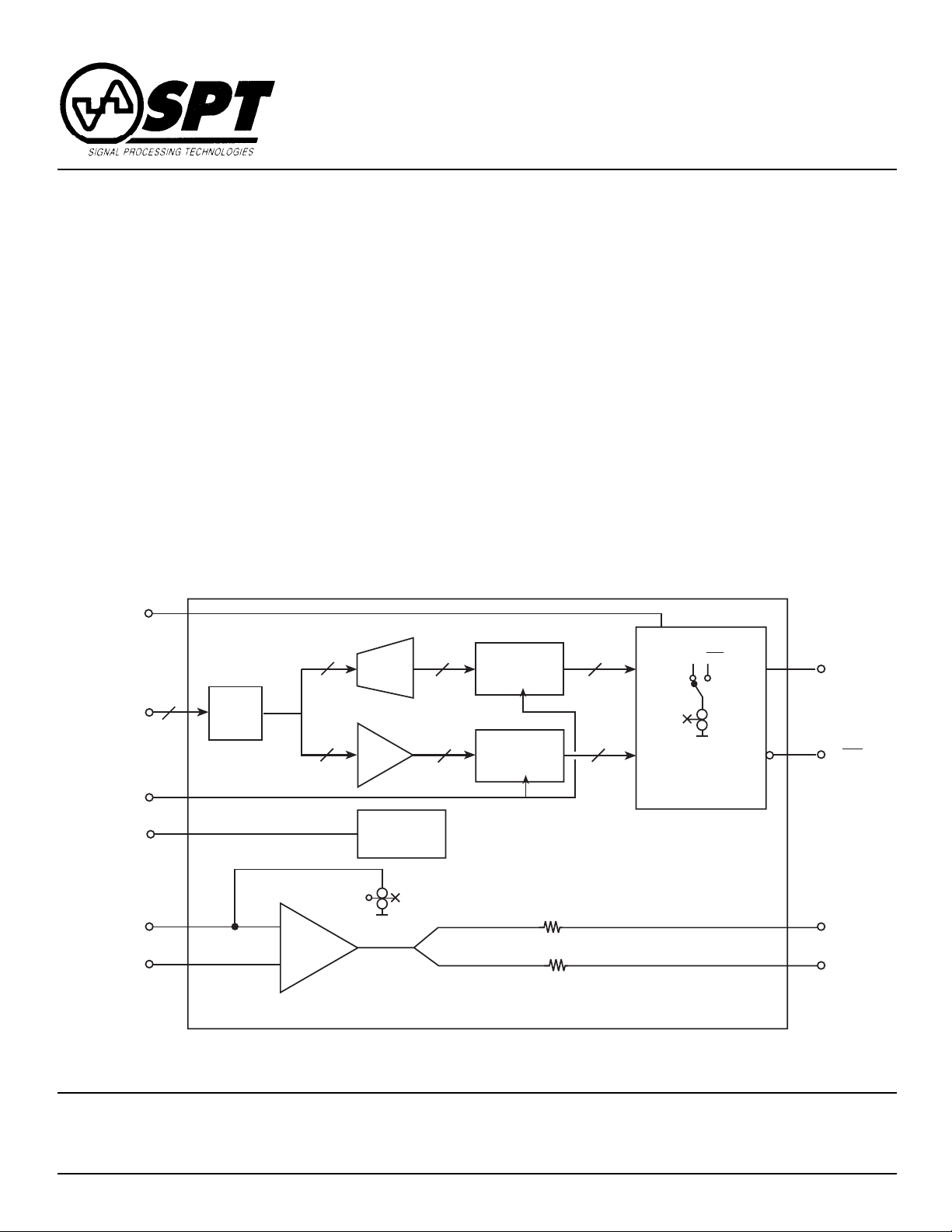
BLOCK DIAGRAM
REF
IN
D15–D12
MSB
Decoder
16 16
APPLICATIONS
• High-precision arbitrary waveform generation
• Test and measurement instrumentation
• Digital waveform synthesis
• Microwave and satellite modems
• Disk drive test equipment
• Industrial process control
• Military applications
has a very high-speed update rate of up to 200 MHz and is
ECL compatible. It has an ultrafast settling time of 25 ns to
0.01% and 35 ns to 0.0008%.
The SPT5510 operates over an industrial temperature
range of –40 °C to +85 °C and is available in a 10 x 10 mm,
44-lead metric quad flat pack (MQFP) plastic package.
I
I
OUT
MSB Latch
OUT
I
OUT
Digital Inputs
D15–D0
CLK
BG
OUT
R
SET
AMP
INB
Phone: (719) 528-2300 FAX: (719) 528-2370 Website: http://www.spt.com E-Mail: sales@spt.com
16
Input
Latch
D11–D0
+
Ref
Amp
–
LSB
Buffer
Bandgap
Reference
Reference
Cell
Bias
12
LSB Latch
Bias
12
Current
Cells
20
10
Signal Processing Technologies, Inc.
4755 Forge Road, Colorado Springs, Colorado 80907, USA
I
OUT
AMP
AMP
OUT
CC
Page 2

ABSOLUTE MAXIMUM RATINGS (Beyond which damage may occur)
1
Supply Voltages
Negative supply voltage (VEE) .................................–7 V
A/D ground voltage differential................................0.5 V
Input Voltages
Digital input voltage (D15–D0, Clock)... ...........–2.5 to 0 V
Ref amp input voltage range..........................–2.5 to 0 V
Reference input voltage range (Ref In)...... V
to –2.5 V
EE
Output Currents
Bandgap reference output current .....................±500 µA
Ref amplifier output current................................ ±2.5 mA
Temperature
Operating temperature............................... –40 to +85 °C
Junction temperature .......................................... +150 °C
Lead, soldering (10 seconds) ............................. +250 °C
Storage ....................................................–65 to +150 °C
Note: 1. Operation at any Absolute Maximum Rating is not implied. See Electrical Specifications for nominal operating
conditions.
ELECTRICAL SPECIFICATIONS
TA= 25 °C, VEE=–5.2 V ±5%, 50% duty cycle clock, unless otherwise specified.
TEST TEST SPT5510
PARAMETERS CONDITIONS LEVEL MIN TYP MAX UNITS
DC Performance
Resolution 16 Bits
Differential Linearity VI –1.95 ±0.6 1.95 LSB
Differential Linearity T
Integral Linearity VI –1.95 ±0.75 1.95 LSB
Integral Linearity T
Integral Linearity Drift IV –0.2 0.2 LSB/°C
Offset Drift T
Monotonicity V 15 Bits
Output Capacitance V 10 pF
Gain Error I –2 0.4 2 % FS
Gain Error Tempco With Ext Reference V 50 ppm FS/°C
Gain Error Tempco With Internal Bandgap Ref V 50 ppm FS/°C
Offset Error I –4 4 µA
Compliance Voltage IV –1.2 2 V
Output Resistance IV 0.88 1.1 1.32 kΩ
Dynamic Performance
Conversion Rate IV 200 MHz
Settling Time t
Delay Time t
Glitch Energy V 30 pV-s
Full Scale Output Current With On-Chip References V 19 mA
Rise Time/Fall Time R
Spurious Free Dynamic Range
ƒ
=5 MHz; ƒ
OUT
ƒ
=10 MHz; ƒ
OUT
1
Measured at 0 V output using I-V.
2
Measured as voltage settling for mid-scale transition; RL = 50 Ω.
1
MIN–TMAX
MIN–TMAX
MIN–TMAX
2
ST
Settling to ±0.01% V 25 ns
Settling to ±0.0008% V 35 ns
D
= 50 Ω V2ns
L
=30 MHz 10 MHz Span V 84 dB
CLOCK
=100 MHz 10 MHz Span V 76 dB
CLOCK
IV –4.0 ±1.0 4.0 LSB
IV –4.0 ±1.5 4.0 LSB
IV –2.5 2.5 ppm FS/°C
V2ns
SPT
SPT5510
2 9/27/00
Page 3

ELECTRICAL SPECIFICATIONS
TA= 25 °C, VEE=–5.2 V ±5%, 50% duty cycle clock, unless otherwise specified.
TEST TEST SPT5510
PARAMETERS CONDITIONS LEVEL MIN TYP MAX UNITS
Power Supply Requirements
Negative Supply Current (–5.2 V) T
Nominal Power Dissipation V 600 800 mW
Power Supply Rejection Ratio ∆V Supply = ±5 % I –0.6 ±0.002 0.6 % FS
Voltage Input and Control
Bandgap Reference Voltage V –1.2 V
Bandgap Output Current T
Ref Amp Bandwidth
3
Ref Amp Input Current V 16 µA
Ref Amp Output Current V 200 µA
Ref In Operating Voltage V –3.4 V
Digital Inputs
Logic 1 Voltage T
Logic 0 Voltage T
Logic 1 Current –0.8 V V 2.5 µA
Logic 0 Current –1.8 V V 0 µA
Input Capacitance V 3 pF
Input Setup Time (tS) IV 3.0 ns
Input Hold Time (t
Clock Pulse Width (t
3
Ref Amp Bandwidth is limited by its compensation network
) IV 0.5 ns
H
) IV 1.5 ns
PWH
–T
MIN
MAX
=25 °C ±10 °C IV –110 16 220 µA
A
VI 115 150 mA
V 40 MHz
MIN
MIN
–T
–T
MAX
MAX
VI –1.0 –0.8 V
VI –1.7 –1.5 V
TEST LEVEL CODES
All electrical characteristics are subject
to the following conditions:
All parameters having min/max specifications are guaranteed. The Test Level
column indicates the specific device
testing actually performed during production and Quality Assurance inspection. Any blank section in the data
column indicates that the specification
is not tested at the specified condition.
TEST LEVEL TEST PROCEDURE
I 100% production tested at the specified temperature.
II 100% production tested at TA = +25 °C, and sample tested at the specified
temperatures.
III QA sample tested only at the specified temperatures.
IV Parameter is guaranteed (but not tested) by design and characterization
data.
V Parameter is a typical value for information purposes only.
VI 100% production tested at T
specified temperature range.
= +25 °C. Parameter is guaranteed over
A
SPT
SPT5510
3 9/27/00
Page 4

THEORY OF OPERATION
The SPT5510 is a segmented 16-bit current-output DAC.
The four MSBs, D15–D12, are decoded to fifteen unit cells
(current sinks). The remaining bits (D11–D0) are binary;
bits D9–D0 are derived from an R-2R ladder. All cells are
laser trimmed for maximum accuracy. The block diagram
shows the basic architecture.
All output cells are always on, with the data determining
whether a given cell’s current is routed from I
This provides nearly constant power dissipation independent of data and clock rate. It also reduces noise transients
on power and ground lines.
The reference loop utilizes an MSB-weighted cell and provides a gain of about 16 to the output. The on-chip reference amplifier has very high open-loop gain and is offset
trimmed to provide a very low temperature drift (typically
<10 ppm/°C gain drift).
OUT
or I
OUT
POWER SUPPLY AND GROUNDING
The SPT5510 requires a single –5.2V power supply. All
supply pins attach to a common on-chip power bus and
should be treated as analog supplies. For best settling performance, each supply pin should be decoupled as shown
in figure 1 – typical interface circuit.
There are three separate on-chip ground busses. DGND
pins should be tied together and connected to system
ground through a ferrite bead. REFGND and OGND pins
.
should be tied directly to the SPT5510’s ground plane and
connected to system ground through a ferrite bead. It is
critical that REFGND and OGND are very tightly coupled,
as any differential signal (dc offset, noise, etc.) will be
transmitted to the output. Two of the OGND pins can be
disconnected from the ground plane and used as sense
lines for a current-to-voltage converter, as shown in the
OUTPUTS section.
Figure 1 – Typical Interface Circuit
Input
Data
C1–C13 — SURFACE MOUNT CERAMIC CHIP
C14–C17 — TANTALUM
R1–R6 — CARBON FILM 1/4 W
R7–R10 — SURFACE MOUNT CERAMIC CHIP
FB — FERRITE BEAD is to be located as closely
to the device as possible.
R10
C13 20 pF
C12 10 pF
C7 .01 µF
50
1
D15
2
D14
3
D13
4
D12
5
D11
6
D10
7
D9
8
D8
25
D7
26
D6
27
D5
28
D4
29
D3
30
D2
31
D1
32
D0
22
9
12
CLK
REFGND
REFGND
DGND
DGND
DGND
DGND
10442433404235
FB
AV
EE
16
OUT
BG
OGND
OGND
R7 1K
17
18
INB
SET
R
AMP
SPT5510
OGND
OGND
37
R1
10
AV
EE
R8 1K
19
15
B
CC
AMP
AMP
EE
AV
AVEEAVEEAVEEAVEEAVEEAVEEAV
39431113142334
R2
10
R9 50
C8 .01 µF
20
21
IN
OUT
REF
AMP
EE
38
R3
R4
10
10
C9 47 pF
C10 47 pF
C11 47 pF
41
I
I
OUT
OUT
36
R5
10
Output
Output
Complementary
R6
10
SPT
2.2 µF
C14
2.2 µF
C15
2.2 µF
C16
2.2 µF
C17
.01 µF
C1
.01 µF
C2
.01 µF
C3
.01 µF
C4
.01 µF
C5
C6 .01 µF
SPT5510
4 9/27/00
Page 5

Wideband decoupling is required for optimum settling performance. This may require several capacitors in parallel,
and series resistors when appropriate, to reduce resonance
effects. Some applications may need only a single capacitor; however, decoupling influences both long- and shortterm settling, so caution is urged. Your application may
require some research to determine the optimum power
supply decoupling network.
DIGITAL INPUTS AND TIMING
Each digital input is buffered, decoded, and then latched
into D flip-flops which drive the output switches. Masterslave flip-flops are not used; thus, there is only a 1/2 clock
period delay (max) from data change to output change. In
this architecture, clock and data edge speeds (i.e., rise/fall
times) may affect data feedthrough. Using a data edge of
approximately 0.8 ns will cause data feedthrough of about
10 pV-s, while a 5 ns data edge will reduce the feedthrough
to about 4 pV-s. Data lines may include series resistors or
RC filters for edge control if desired.
The clock signal controls when the data is latched into the
flip-flops. When the CLK is high, the DAC is in track mode. A
negative going CLK latches the data. If CLK is held low, the
DAC is in hold mode. See figure 2.
Figure 2 – Timing Diagram
t
H
t
D
CLK
DATA
t
S
OUTPUTS
The output is comprised of current sinks, R-2R ladder, and
associated parasitics. See figure 3 for an equivalent output
circuit.
The DAC’s full-scale output current when using the internal
reference amplifier is determined by the voltage at pin
AMP
and the R
INB
resistance. It can be found (to within
SET
an LSB) by using the following formula:
I
FS = (AMP
OUT
INB/RSET
) x 16
The inputs determine whether the current from each sink
comes from I
Code (D15 is MSB) I
0 (zero scale) No current All current
32768 (mid-scale) I
65535 (full-scale) All current No current
OUT
or I
as follows:
OUT
OUT
= I
OUT
I
OUT
OUTIOUT
= I
OUT
Differential outputs facilitate maximum noise rejection and
signal swing. The DAC is trimmed using a current to voltage
(I-V) converter which provides a virtual ground at the outputs and includes sense lines to mitigate the impact of bus
drops. Operating into a load other than a virtual ground will
introduce a slight bow at the output. This bow is related to
the current sinks’ finite output impedance and ladder
impedance.
An example circuit using an I-V converter is shown in figure
4. Note that resistor and op-amp self heating over the DAC’s
full-scale range will introduce additional temperature dependence. The op-amp and feedback resistor must both have
very low tempcos if the DAC’s intrinsic gain drift is to be
maintained. A sense line helps reduce wire effects – both IR
loss and temperature drift.
I
OUT
I
OUT
tH = hold time
tD = time to output valid
tS = setup time
tST = settling time
Figure 3 – Equivalent Output Circuit
I
OUT
or
I
OUT
AV
1.1k
EE
SPT
t
10 pF
Figure 4 – I-V Converter
ST
OGND
I
OUT
OGND
OGND
I
OUT
OGND
BNC
”
"I
OUT
250
GND
–
+
+
–
GND
250
BNC
"I
"
OUT
SPT5510
5 9/27/00
Page 6

The feedback resistor should be matched to R
to reduce
SET
gain drift. Also, the op amp’s ground reference should be
the same as R
’s to reduce gain and offset errors. A com-
SET
posite amplifier may be required to obtain optimal dc performance. A differential circuit may be used; a common heat
sink covering both sides (op amps and resistors) will help
reduce temperature effects.
Achieving good settling performance requires careful board
layout with multiple decoupling circuits and very clean
power and ground routing. It is important that digital switching currents do not flow across analog input (REFIN) and
output signals. Terminations must be broadband and near
the device. Measuring settling performance is quite challenging and requires several test systems to ensure settling
errors from the instruments are not included.
Dynamic performance characteristics (e.g., settling, rise
and fall times, etc.) were measured with the outputs terminated to ground through 50 Ω resistors. SFDR was determined using a transformer to convert the output from differential to single-ended as shown in figure 5. The SPT5510 is
designed primarily for step and settle or narrowband RF
applications. The second harmonic generally dominates
wideband SFDR measurements, although close-in spurs
are very small.
Figure 5 – Transformer Output Circuit
I
OUT
BANDGAP VOLTAGE REFERENCE
The on-chip bandgap voltage reference is designed to bias
the non-inverting input of the reference amplifier (AMP
through a resistor equal to R
to help compensate the ref-
SET
INB
erence amplifier (see the following section). If the bandgap
voltage is required by another DAC, or elsewhere in the system, it must be buffered with a precision op amp configured
as a high impedance (e.g., unity gain follower) buffer. A
resistor, or RC filter, plus a ferrite bead will help isolate the
output from the reference amplifier’s compensation and
high-frequency charge pulses produced during operation.
The output should always be very carefully checked for
oscillations using a sensitive, wideband oscilloscope and
spectrum analyzer.
REFERENCE AMPLIFIER
The reference amplifier is a highly temperature-stable driver
to bias the precision current sinks. The reference amplifier
should only be used to drive REFIN. Additional loads will
change the amplifier’s compensation, which can lead to
instability and other settling issues.
There are two reference amplifier outputs: AMP
AMPCC. AMP
has a 20 ohm series resistor between the
OUT
output of the reference amplifier and the AMP
OUT
OUT
and
pin;
AMPCC has a 10 ohm resistor. These parallel outputs aide
compensation and decoupling. The open-loop output
impedance is approximately 1200 ohms.
)
25
25
I
OUT
Figure 6 – Reference Amplifier Circuit
R
SET
0.01 µF
1 kΩ
1 kΩ
16
17
18
BG
+
Ref Amp
–
OUT
15
AMP
B
V
EE
0.01 µF
Reference amplifier compensation is key to achieving high
performance. Without proper compensation, oscillations
that affect accuracy and settling time will occur. Figure 6
shows a typical reference amplifier compensation circuit.
Note that several small value capacitors are used from
REFIN to ground. This is to provide suitably low impedance
SPT5510 DAC
20 Ω
10 Ω
All components are ceramic chip-type.
20
19
AMP
AMP
OUT
CC
50Ω
10 pF
20 pF
C1 C2 C3
47 pF each
21
REF
IN
SPT
SPT5510
6 9/27/00
Page 7

around 300 MHz, the amplifier’s phase crossover point. The
unity-gain bandwidth is roughly 700 MHz. Larger value
capacitors exhibit lower self-resonance frequency and thus
may not adequately compensate the reference amplifier.
Large capacitors may also introduce low frequency tails
which increase settling time. The DAC itself exhibits very
broadband switching spikes (charge kickback) at the R
SET
node, which can contribute to amplifier instability if not suppressed. Note that the AMP
input must not be directly
INB
bypassed, as this will short all feedback to ground, leading
to severe oscillation.
Compensation must be optimized for each application. As
with any high-speed, high-resolution design, attention must
be paid to grounding, decoupling, and parasitic elements
that may cause instability. It may be wise to use a guard
ring, and/or clear the board ground, around the reference
amplifier’s inputs. All traces must be short, and capacitors
with high self-resonance must be used.
LONG-TERM STABILITY
VERSUS TEMPERATURE
As with all high-speed, high-resolution digital-to-analog converters, the initial accuracy of the device will degrade with
both time and temperature. The graph shown in figure 7 can
be used to determine the expected change in linearity performance over time when the device is operated at various
ambient temperatures. This graph shows how long it will
take for the SPT5510 linearity to change by 8 ppm (or 1/2
LSB) at any operating temperature. The top curve shown
represents integral nonlinearity (ILE) changes; the bottom
curve shows differential nonlinearity (DLE) changes.
Figure 7 – Linearity Performance over Time
7
1000 years
10
6
100 years
10
Compensation is perhaps the most challenging aspect of
setting up the SPT5510. By slowly switching a full-scale
data input (generating a low-frequency square wave), with
appropriate clock timing, the DAC’s output can be observed
using a suitable oscilloscope and spectrum analyzer to
observe and suppress any oscillations caused by board and
decoupling parasitics. Consult SPT Applications for further
assistance if required.
PACKAGE OUTLINE
A
B
Pin 1
G
Index
C
E F
H
I
J
44-Lead MQFP
D
K
5
10
(Hours)
4
1 year
10
ILE
3
10
1 month
2
10
0 20 40 60 80 100 120
Expected time required to produce an 8 ppm (1/2 LSB) linearity
(ILE or DLE) shift as a function of temperature.
Temperature (°C)
DLE
INCHES MILLIMETERS
SYMBOL MIN MAX MIN MAX
A 0.5098 0.5295 12.95 13.45
B 0.3917 0.3957 9.95 10.05
C 0.3917 0.3957 9.95 10.05
D 0.5098 0.5295 12.95 13.45
E 0.0311 0.0319 0.79 0.81
F 0.0118 0.0177 0.30 0.45
G 0.0768 0.0827 1.95 2.10
H 0.0039 0.0098 0.10 0.25
I 0.0287 0.0406 0.73 1.03
J 0.0630 REF 1.60 REF
K0° 7° 0° 7°
SPT
SPT5510
7 9/27/00
Page 8

PIN ASSIGNMENTS
OGND
AV
EE
43
13
AV
EE
AV
EE
I
OUT
41
42
15
14
AMP
B
(MSB) D15
D14
D13
D12
D11
D10
D9
D8
CLK
DGND
AV
DGND
44
1
2
3
4
5
6
7
8
9
10
11
EE
12
REFGND
OGND
AV
EEAVEE
39
40
SPT5510
44-Pin
MQFP
17
16
R
BG
SET
OUT
INB
38
18
AMP
OGND
37
19
AMP
CC
I
OUT
36
20
AMP
OUT
OGND
35
21
REF
IN
AV
EE
34
33
32
31
30
29
28
27
26
25
24
23
22
REFGND
DGND
D0 (LSB)
D1
D2
D3
D4
D5
D6
D7
DGND
AV
EE
PIN FUNCTIONS
NAME FUNCTION
D15–D0 Digital Input Bits – all inputs high sends all
current to I
CLK Clock – latches D flip-flops
I
OUT
I
OUT
BG
AMP
R
SET
OUT
INB
Analog Current Output
Complementary Analog Current Output
Bandgap Voltage Reference
Ref Amp’s Inverting Input
Ref Amp’s Non-Inverting Input – connection for
reference-current-setting resistor, nominally
1kΩ to ground
AMP
OUT
Bias Voltage for Output Current Switches –
drives REF
compensation)
REF
IN
Bias Voltage Node for Output Current Switches
– driven by AMP
AMP
AMP
B
CC
Used to Decouple Ref Amp’s Circuits to AV
AMP
OUT
compensation
, none to I
OUT
(on-chip 20 Ω resistor for
IN
OUT
OUT
plus on-chip 10 Ω series resistor for
EE
AV
EE
Negative Supply – –5.2 V
DGND Digital Ground Return
OGND Output Ground Return
REFGND Reference Amplifier Ground Return
ORDERING INFORMATION
PART NUMBER TEMPERATURE RANGE PACKAGE
SPT5510SIM –40 to +85 °C 44L MQFP
Signal Processing Technologies, Inc. reserves the right to change products and specifications without notice. Permission is hereby expressly
granted to copy this literature for informational purposes only. Copying this material for any other use is strictly prohibited.
WARNING – LIFE SUPPORT APPLICATIONS POLICY – SPT products should not be used within Life Support Systems without the specific
written consent of SPT. A Life Support System is a product or system intended to support or sustain life which, if it fails, can be reasonably
expected to result in significant personal injury or death.
Signal Processing Technologies believes that ultrasonic cleaning of its products may damage the wire bonding, leading to device
failure. It is therefore not recommended, and exposure of a device to such a process will void the product warranty.
SPT5510
SPT
8 9/27/00
 Loading...