

Page 1
SPT5420
13-BIT, OCTAL D/A CONVERTER
TECHNICAL DATA
JUNE 26, 2001
FEATURES
• 13-bit resolution
• Pin compatible with AD7839
• Eight DACs in one package
• Buffered voltage outputs
• Wide output voltage swing VDD–2.5 V to VSS+2.5 V
• 15 µs settling time to ±0.5 LSB
• Double-buffered digital inputs
• Microprocessor and TTL/CMOS compatible
GENERAL DESCRIPTION
The SPT5420 contains eight 13-bit digital-to-analog
CMOS converters designed primarily for automatic test
equipment applications. It uses novel circuit topology to
convert the 13-bit digital inputs into output voltages which
are proportionate to the applied reference voltages. Each
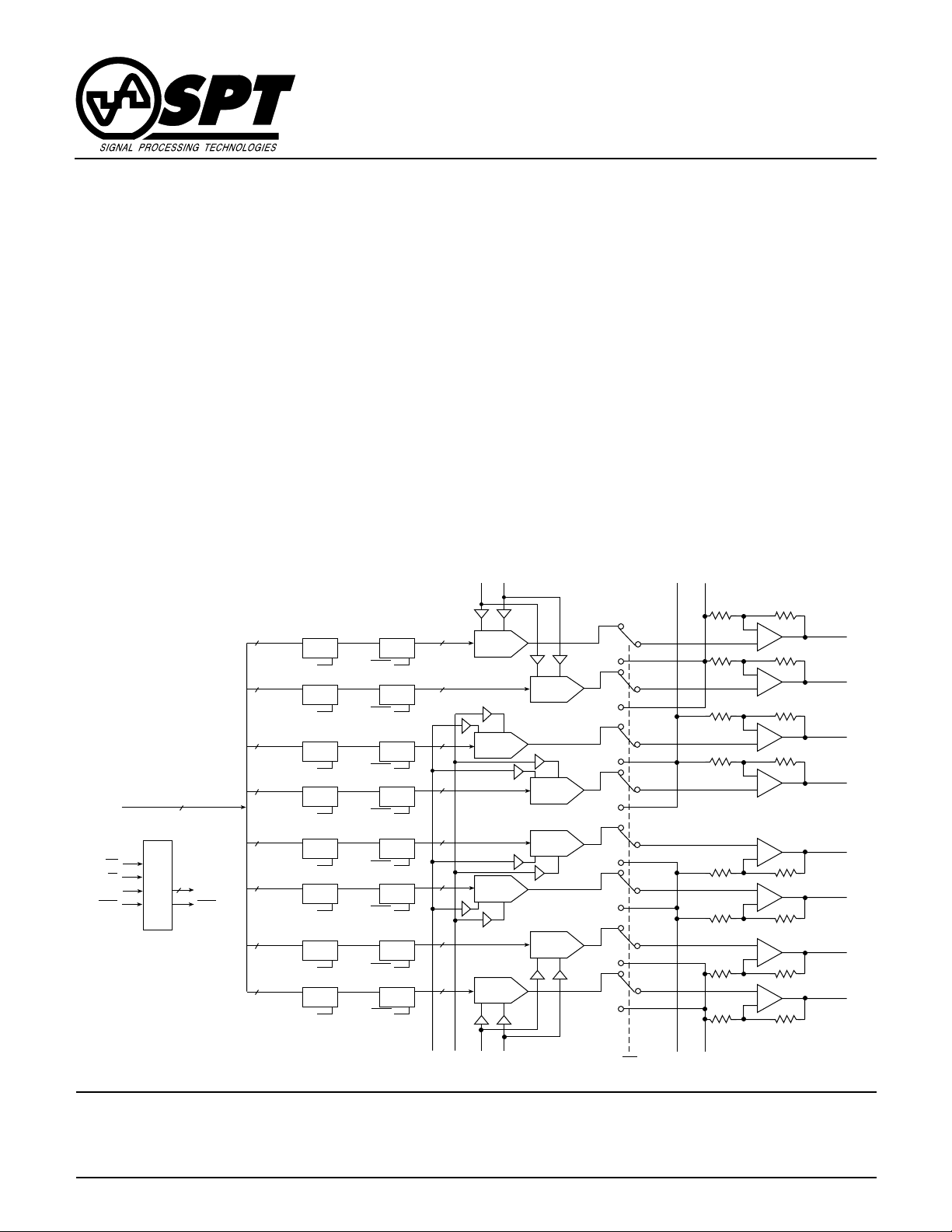
BLOCK DIAGRAM
D0D12
A0A2
LDAC
WR
13 13
13 13
13 13
13
13
13
CS
Control
Logic
8
LEA0LEA7
LDAC
13
DQ
0A 0B
LE
LEA0
DQ
1A 1B
LE
LEA1
DQ
2A 2B
LE
LEA2
DQ
3A 3B
LE
LEA3
DQ
4A 4B
LE
LEA4
Q
D
5A 5B
LE
LEA5
DQ
LDAC
DQ
LDAC
DQ
LDAC
DQ
LDAC
DQ
LDAC
D
LDAC
LE
LE
LE
13
LE
13
LE
13
Q
LE
APPLICATIONS
• Automatic test equipment
• Instrumentation
• Process control
DAC’s full-scale output voltage and output voltage offset
are adjustable with analog inputs (RGND, V
The SPT5420 operates over an industrial temperature
range of –40 °C to +85 °C and is availab le in a 10 x 10 mm,
44-lead metric quad flat pack (MQFP) plastic package.
V
REFT01VREFB01
DAC0
DAC2
DAC5
DAC1
DAC3
DAC4
RGND
RGND
01
23
-
+
-
+
-
+
-
+
+
-
+
-
REFB
, V
REFT
VOUT0
VOUT1
VOUT2
VOUT3
VOUT4
VOUT5
).
LE
LE
V
REFT2345
13
13
V
REFB2345VREFT67
DAC7
V
REFB67
DAC6
CLR
RGND
+
-
+
-
RGND
67
45
13
13
DQ
6A 6B
LE
LEA6
DQ
7A 7B
LE
LEA7
DQ
LDAC
DQ
LDAC
Signal Processing Technologies, Inc.
4755 Forge Road, Colorado Springs, Colorado 80907, USA
Phone: 719-528-2300 Fax: 719-528-2370 Web Site: http://www .spt.com e-mail: sales@spt.com
VOUT6
VOUT7
Page 2

ABSOLUTE MAXIMUM RATINGS (Beyond which damage may occur)1 25 °C
Supply Voltages
VCC........................................................................+6 V
VDD......................................................................+15 V
Temperature
Operating Temperature .......................... –40 to +85 °C
Storage ................................................ –65 to +150 °C
VSS...................................................................... –15 V
Input Voltages
V
.................................... VSS –0.3 V to VDD +0.3 V
REFT
V
................................... VDD +0.3 V to VSS –0.3 V
REFB
Note: 1. Operation at any Absolute Maximum Rating is not implied. See
Electrical Specifications for proper nominal applied conditions
in typical applications.
Digital inputs....................................–0.3 V to VCC +0.3 V
ELECTRICAL SPECIFICATIONS
TA = T
PARAMETERS CONDITIONS LEVEL MIN TYP MAX UNITS
Accuracy
Reference Inputs
RGND Inputs
to T
MIN
, VCC = +5.0 V, VDD = +11.5 V, VSS = –8.0 V, V
MAX
REFT
=3.5 V , V
= –1.5 V, RL = +10 kΩ, CL = 50 pF, unless otherwise specified.
REFB
TEST TEST SPT5420
Resolution VI 13 Bits
Integral Linearity Error (ILE) VI –2.0 ±0.5 +2.0 LSB
Differential Linearity Error (DLE) VI –1.0 ±0.3 +1.0 LSB
Zero-Scale Error VI –25 +25 mV
Full Scale Error VI –25 +25 mV
Gain Error VI –25 +25 mV
Input Current IV ±100 nA
V
V
REFT
REFB
1
2
VI 0 +3.5 +5.0 V
VI –5.0 –1.5 0 V
DC Input Impedance V 60 kΩ
Input Range IV –2.0 2.0 V
Output Characteristics
Output Swing
3,4
VI +7/–3 V
Short Circuit Current IV 1 5 mA
Resistive Load VI 5 kΩ
DC Output Impedance IV 1.0 Ω
Digital Inputs
Logic 1 Voltage VI 2. 4 V
Logic 0 Voltage VI 0.8 V
Maximum Input Current VI –10 10 µA/pin
Input Capacitance V 10 pF
Notes:
1. V
< 8 V + (VSS x 0.5); e.g., if VSS = –8 V, then V
REFT
2. V
> (VDD x 0.5) – 9.5 V; e.g., if VDD = 11 V, then V
REFB
3. VSS + 2.5 V ≤ V
VSS + 2.5 V ≤ V
4. V
= 2 X (V
OUT
≤ VSS + 16.0 V for 18.5 V ≤ VDD – VSS ≤ 20.0 V
OUT
≤ VDD – 2.5 V f or VDD – VSS ≤ 18.5 V
OUT
+[V
REFT
– V
REFB
REFB
INPUT CODE
] X
8192
REFT
REFB
) – V
< 4 V
> –4 V
RGND
SPT
SPT5420
2 6/26/01
Page 3

ELECTRICAL SPECIFICATIONS
TA = T
MIN
to T
, VCC = +5.0 V, VDD = +11.5 V, VSS = –8.0 V , V
MAX
REFT
=3.5 V, V
=–1.5 V, RL = +10 kΩ, CL = 50 pF, unless otherwise specified.
REFB
TEST TEST SPT5420
PARAMETERS CONDITIONS LEVEL MIN TYP MAX UNITS
Power Requirements
V
Supply Voltage (Digital) IV 4.75 5 5.25 V
CC
Supply Voltage (Analog)
V
DD
Supply Voltage (Analog)
V
SS
I
Supply Current VI 0.5 mA
CC
Supply Current Outputs Unloaded VI 5 10 mA
I
DD
Supply Current Outputs Unloaded VI 5 10 mA
I
SS
Power Supply Rejection Ratio ∆V
1,2
1,2
VI 5 11.5 12.5 V
VI –12.5 –8 –5V
/ ∆Full Scale IV 80 dB
DD
/ ∆Full Scale IV 80 dB
∆V
SS
Dynamic Performance
Output Settling Time
3
(Full Scale Change to ±0.5 LSB) CL ≤ 220 pF IV 15 µs
Slew Rate V 2.0 V/µs
Glitch Impulse V 35 nV-s
Channel to Channel Isolation V 100 dB
DAC to DAC Crosstalk V 40 nV-s
Digital Crosstalk V 1 nV-s
Digital Feedthrough V 1 nV-s
Timing Characteristics
(See page 4) IV
1. Supplies should provide 2.5 V headroom above and below max output s wing.
2. VDD – VSS ≤ 20 V
3. Output can drive 10,000 pF without oscillation, but with settling time degradation.
DEFINITION OF SELECTED TERMINOLOGY
Channel-to-Channel Isolation
Channel-to-Channel isolation refers to the proportion of input signal from one DAC’s reference input that appears at the output of
the other DAC. It is expressed in dBs.
DAC-to-DAC Crosstalk
DAC-to-DAC crosstalk is defined as the glitch impulse that appears at one DAC’s output due to both the digital change and subsequent analog output change at any other DAC. It is specified in nV-s.
Digital Crosstalk
The glitch impulse transferred to one DAC’s output due to a change in digital input code of any other DAC. It is specified in nV-s.
Digital Feedthrough
Digital feedthrough is the noise at a DAC’s output caused by changes to D0–D12 while WR is high.
TEST LEVEL CODES
All electrical characteristics are subject to the
following conditions:
All parameters having min/max specifications
are guaranteed. The Test Level column indicates the specific device testing actually performed during production and Quality Assurance inspection. Any blank section in the data
column indicates that the specification is not
tested at the specified condition.
LEVEL TEST PROCEDURE
I 100% production tested at the specified temperature.
II 100% production tested at T
specified temperatures.
III QA sample tested only at the specified temperatures.
IV Parameter is guaranteed (but not tested) by design and characteri-
zation data.
V Parameter is a typical value for information pur poses only.
VI 100% production tested at TA = +25 °C. Parameter is guaranteed
over specified temperature range.
= +25 °C, and sample tested at the
A
SPT
SPT5420
3 6/26/01
Page 4

TIMING CHARACTERISTICS
t
11
t
9
CLR
V
OUT
Figure 1a – Timing Diagram: Latched Mode
(LDAC Strobed)
A0A2
CS
WR
D0D12
V
OUT
LDAC
t
1
t
3
t
5
t
4
t
2
t
6
t
t
7
8
t
9
t
10
Figure 1b – Timing Diagram: Transparent Mode
(LDAC Held Low)
t
2
t
6
t
t
7
8
A0A2
CS
WR
D0D12
V
OUT
t
1
t
3
t
5
t
4
t
9
SPT
PARAMETER SYMBOL MIN TYP MAX UNIT
Address V alid to WR Setup t
Address Valid to WR Hold t
CS Pulse Width Low t
WR Pulse Width Low t
CS to WR Setup t
WR to CS Hold t
Data Setup t
Data Hold t
Settling Time
LDAC Pulse Width Low t
CLR Pulse Activation t
1
1
2
3
4
5
6
7
8
t
9
10
11
20 ns
0ns
50 ns
50 ns
0ns
0ns
25 ns
0ns
15 us
50 ns
300 ns
NOTES:
All digital input rise and fall times are measured from 10% to 90% of +5 V.
t
= tf = 5 ns.
r
1. R
= 10 kΩ
L
C
≤ 220 pF
L
4 6/26/01
SPT5420
Page 5

VOLTAGE REFERENCES AND
ANALOG GROUND INPUTS
ANALOG OUTPUTS VS DIGITAL INPUT
CODE
Three V
REFTXX
and three V
REFBXX
inputs set the output
range of the three corresponding groups of DACs
(0 and 1; 2 through 5; 6 and 7). Four RGNDXX inputs set
the output offset voltage of the four corresponding groups
of DA Cs (0 and 1; 2 and 3; 4 and 5; 6 and 7). The formula
for output swing and offset is presented in the “Analog
Outputs” section below.
DAC ADDRESSING AND LATCHING
Each DA C has an input latch which receives data from the
data bus, and a DAC latch which receives data from the
input latch. The analog output of each DAC corresponds
to the data in its DA C latch. One of the eight input latches
is addressed by the address lines A(2:0) according to
Table I. While CS and WR are low, the addressed input
latch is transparent and the seven other input latches are
latched. Bringing CS or WR high latches data into the addressed input latch. While LDAC is low, all eight DAC
latches are transparent. Bringing LDAC high latches data
into the DA C latches. While CS, WR and LDAC are lo w , both
latches are transparent and input data is transferred
directly to the selected DA C. While CLR is low, all D A C outputs are set to their corresponding RGNDXX. Bringing CLR
high returns each DAC’s output to the voltage correspond-
ing to the data in each DAC latch.
Table II summarizes this information, and figures 1a and
1b should be referenced for timing limitations.
POWER SUPPLY SEQUENCING
The sequence in which VDD, VSS and VCC come up is not
critical. The reference inputs, V
REFTXX
come on only after VDD and VSS have been established.
However, they may be turned on prior to VCC. The digital
inputs must be driven only after VDD, VSS and VCC have
been established. Reverse the power-on sequence for
power-down.
and V
REFBXX
, must
The output voltage range is equal to twice the difference
between V
REFTXX
and V
REFBXX
. The output voltage is
given by:
V
OUT
= 2 X (V
REFB
+[V
REFT
– V
REFB
INPUT CODE
] X
8192
) – V
RGND
CODE = 0 – 8191
Table I – DAC Addressing
A2 A1 A0 Latch DAC#
000 0
001 1
010 2
011 3
100 4
101 5
110 6
111 7
Addressed Input
Table II – Control Logic Table
WR CS LDAC CLR Input Latch DAC Latch
0 0 x 1 transparent
1 x x 1 latched x
x 1 x 1 latched x
x x 0 1 x transparent
x x 1 1 x latched
x x x 0 DAC outputs at RGND
Note:
1 . Only the input latch addressed by A(2:0) is transparent.
The other input latches are latched.
1
x
XX
SPT
SPT5420
5 6/26/01
Page 6

TYPICAL PERFORMANCE CHARACTERISTICS
Integral Linearity Error vs Code Differential Linearity Error vs Code
1.00
0.80
0.60
0.40
0.20
0.00
0.20
ILE (LSBs)
0.40
0.60
0.80
1.00
0 1440 2880 4320 5760 7200
I
DD/ISS
8
VDD=12 V
VSS=8 V
7
6
5
Supply Current (mA)
4
40 0 25 70 85
V
V
REFT
REFB
Code
vs Temperature
=+5 V
=5 V
I
DD
I
SS
Temperature °C
0.20
0.00
0.20
0.40
0.60
DLE (LSBs)
0.80
1.00
0 1440 2880 4320 5760 7200
Code
Load Capacitance vs Settling Time
10000
V
=10 V
SWING
1000
100
10
Capacitance (pF)
1
11.20 11.70 12.20 13.90 17.90 26.50 52.00 70.00
Settling Time to ±0.5 LSB (µS)
2 mV/div
SPT
Digital-to-Analog Glitch Impulse DAC to DAC Crosstalk
2 V/div
2 µS
output glitch
code 0FFFH to 1000H
WR
DAC to DAC glitch
2 mV/div
2 µS
code 0FFFH to 1000H
6 6/26/01
SPT5420
Page 7

TYPICAL PERFORMANCE CHARACTERISTICS
digital feedthrough
2 µS
Digital Feedthrough
code 0FFFH to 1000H
2 mV/div
CL=50 pF
R
output
2 V/div
PACKAGE OUTLINE
Slew and Settling Time
=10 kW
L
code 0000H to 1FFFH
1 µS
output
20 mV/div
44-Lead MQFP
A
B
SYMBOL MIN MAX MIN MAX
A 0.5098 0.5295 12.95 13.45
B 0.3917 0.3957 9.95 10.05
Pin 1
Index
C 0.3917 0.3957 9.95 10.05
D 0.5098 0.5295 12.95 13.45
E 0.0311 0.0319 0.79 0.81
F 0.0118 0.0177 0.30 0.45
G 0.0768 0.0827 1.95 2.10
C
D
H 0.0039 0.0098 0.10 0.25
I 0.0287 0.0406 0.73 1.03
J 0.0630 REF 1.60 REF
K0° 7° 0° 7°
E F
G
K
H
I
J
INCHES MILLIMETERS
SPT
SPT5420
7 6/26/01
Page 8

PIN ASSIGNMENTS
23
OUT2
OUT1
RGND
V
V
44
RGND
01
V
V
REFB01
V
REFT01
LDAC
OUT0
V
DD
V
SS
A2
A1
A0
CS
1
CC
WR
V
GND
OUT3
REFB2345
REFT2345
V
V
V
V
Top View
D2
D1
D3
D0 (LSB)
DD
OUT4
V
D4
45
OUT5
V
RGND
D5
D6
OUT6
V
D7
RGND
67
V
OUT7
V
REFB67
V
REFT67
V
SS
CLR
D12 (MSB)
D11
D10
D9
D8
PIN FUNCTIONS
Name Function
DIGITAL CONTROL PINS
CS Chip Select (Active Low)
WR Level Triggered Write Input (Active Low). Used in
conjunction with
input data latches. Data is latched into selected
input data latch on the rising edge of WR.
CLR (Active Low) Analog Clear. Sets the output
voltages to RGND. (Each RGND is common to a
DAC pair.)
CLR is brought back high, the DAC outputs
When
revert back to their original outputs as determined
by the data in their DAC latches.
LDAC When this logic input is taken low, the contents of
the input latches are transferred to their respective
DAC latches. (Active Low) Data is latched on
rising edge.
A0 – A2 Addresses DAC0 to DAC7 for loading the eight
input latches.
D0 – D12 Digital Inputs (D0 = LSB)
ANALOG PINS
V
REFT01
V
REFT2345
V
REFT67
V
REFB01
V
REFB2345
V
REFB67
RGND
RGND
RGND
RGND
V
OUT0–7
Top Reference Voltage for DACs 0 and 1
Top Reference Voltage for DACs 2, 3, 4 and 5
Top Reference Voltage for DACs 6 and 7
Bottom Reference Voltage for DACs 0 and 1
Bottom Reference Voltage for DACs 2, 3, 4 and 5
Bottom Reference Voltage for DACs 6 and 7
Reference Ground for Output Amplifiers 0 and 1
01
Reference Ground for Output Amplifiers 2 and 3
23
Reference Ground for Output Amplifiers 4 and 5
45
Reference Ground for Output Amplifiers 6 and 7
67
Output Voltage Pins for DAC0 – DAC7
POWER SUPPLY PINS
V
CC
V
DD
V
SS
Digital +5 V Supply
Analog +11.5 V Supply (Nominal)
Analog –8 V Supply (Nominal)
GND Ground
CS to write data to the SPT5420
CLR does not reset the digital latches.
ORDERING INFORMATION
PART NUMBER TEMPERATURE RANGE PACKAGE
SPT5420SIM –40 to +85 °C 44L MQFP
Signal Processing Technologies, Inc. reserves the right to change products and specifications without notice. Permission is hereby
expressly granted to copy this literature for informational purposes only. Copying this material for any other use is strictly prohibited.
WARNING – LIFE SUPPORT APPLICATIONS POLICY – SPT products should not be used within Life Support Systems without
the specific written consent of SPT. A Life Support System is a product or system intended to support or sustain life which, if it fails,
can be reasonably expected to result in significant personal injury or death.
Signal Processing Technologies believes that ultrasonic cleaning of its products may damage the wire bonding, leading to device
failure. It is therefore not recommended, and exposure of a device to such a process will void the product warranty.
SPT5420
SPT
8 6/26/01
 Loading...