

Page 1
SPT5230
10-BIT, 36 MWPS TRIPLE VIDEO DAC
FEATURES
• 10-Bit Triple Video Digital-to-Analog Converter
• Output Full-Scale Voltage 0.5 to 2.0 Vp-p
• 36 MWPS Operation (typ)
• Low Power: 280 mW (1 Vp-p Output)
• 5 V Monolithic CMOS
• 52-pin QFP Package (10mm x 10mm, 0.65 mm pitch)
GENERAL DESCRIPTION
The SPT5230 is a 10-bit, 36 MWPS triple video digital-toanalog converter specifically designed for high performance,
high resolution color graphics monitor applications and video
processing applications. A single external resistor controls
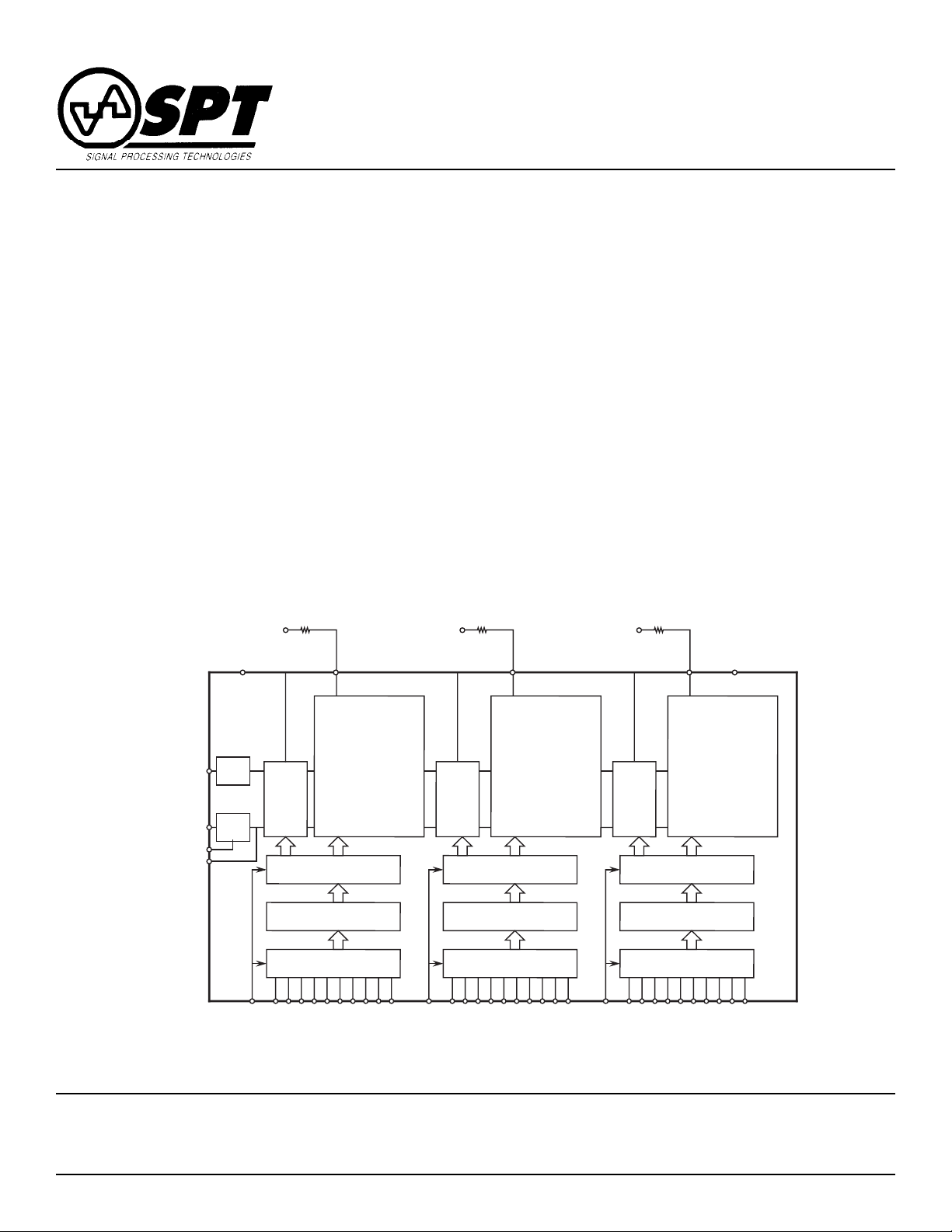
BLOCK DIAGRAM
R
OUT
AV
DD
AV
DD
I
OR
AV
DD
APPLICATIONS
• Desktop Video Processing
• CCIR-601 Video Signal Processing
• RGB Color Monitors
• Image Processing
• Direct Digital Synthesis
the full-scale output current. The differential linearity errors of
the DACs are guaranteed to be a maximum of ±1.0 LSB over
the full temperature range. The device is available in a 52lead QFP package over the commercial temperature range.
G
OUT
I
OG
B
DD
OUT
I
OB
V
SSA
AV
V
V
REF1
REF2
V
CS2
V
CS1
Current
V
REF
Current
Switch
Cell
Array
(Cell 4)
V
CS
Switch Cell
Array (Cell 255)
Current
Switch
Cell
Array
(Cell 4)
Latch
Decoder
Latch
DR6
DR7
CLKR
DR8
(MSB) DR9
DR5
DR4
DR3
DR2
DR1
(LSB) DRØ
CLKG
DG8
(MSB) DG9
Current
Switch Cell
Array (Cell 255)
Latch
Decoder
Latch
DG3
DG4
DG5
DG6
DG7
DG2
DG1
(LSB) DGØ
Current
Switch
Array
(Cell 4)
CLKB
Cell
DB8
(MSB) DB9
Current
Switch Cell
Array (Cell 255)
Latch
Decoder
Latch
DB6
DB7
DB5
DB4
DB3
DB2
DB1
(LSB) DBØ
Signal Processing Technologies, Inc.
4755 Forge Road, Colorado Springs, Colorado 80907, USA
Phone: (719) 528-2300 FAX: (719) 528-2370 Website: http://www.spt.com E-Mail: sales@spt.com
Page 2

ABSOLUTE MAXIMUM RATINGS (Beyond which damage may occur)
Supply Voltages
AV
(measured to AVSS)...........................–0.3 to 7.0 V
DD
Output Current
I
...........................................................................
OUT
1
0 to 14 mA
Input Voltage
Clock and Data ......................................... AVSS to AV
DD
Temperature
Operating, ambient ........................................ 0 to +70 °C
Storage ...................................................–55 to + 125 °C
Note: 1. Operation at any Absolute Maximum Rating is not implied. See Electrical Specifications for proper nominal applied
conditions in typical applications.
ELECTRICAL SPECIFICATIONS
f
= 27 MWPS, AVDD = 5.0 V, Output Pull-Up Load = 75 Ω, TA = 25 °C, AVSS = 0.0 V
CLK
TEST TEST
PARAMETERS CONDITIONS LEVEL MIN TYP MAX UNITS
DC Performance
Resolution 10.0 Bits
Differential Linearity T
Integral Linearity I –2.5 2.0 LSB
Analog Outputs
Output Voltage Range V
Conversion Rate I 27 36 MWPS
Output Offset Voltage I 2.4 14 mV
Signal-to-Noise Ratio I 46 52 dB
Settling Time
Propagation Delay (t
Crosstalk I –49 –54 dB
FS Control Voltage (V
Digital Inputs and Timing
Input Current, Logic High V
Set-Up Time, Data and Controls (t
Hold Time, Data and Controls (t
Clock Duty Cycle V 40 60 %
Power Supply Requirements
Supply Voltage I 4.75 5.25 V
Supply Current 1 Vp-p Output IV 56 mA
Power Dissipation 1 Vp-p Output IV 280 mW
1
Full-scale settling time to within ±2% of full scale.
1
) V 10 12 ns
pd
) V 2.0 4.0 V
CS2
Logic Low V
)I5ns
S
) I 10 ns
h
= T
A
CS2
IH
= 0 V I –5 µA
IL
2 Vp-p Output I 100 mA
2 Vp-p Output I 485 500 mW
to T
MIN
= +2.1 V I 3.0 5.0 V
= 5 V I 5 µA
MAX
I –1.0 1.0 LSB
I1623ns
TEST LEVEL CODES
All electrical characteristics are subject to the
following conditions:
All parameters having min/max specifications
are guaranteed. The Test Level column indicates the specific device testing actually performed during production and Quality Assurance inspection. Any blank section in the data
column indicates that the specification is not
tested at the specified condition.
SPT
TEST LEVEL
I
II
III
IV
V
VI
2 5/1/00
TEST PROCEDURE
100% production tested at the specified temperature.
100% production tested at TA=25 °C, and sample
tested at the specified temperatures.
QA sample tested only at the specified temperatures.
Parameter is guaranteed (but not tested) by design
and characterization data.
Parameter is a typical value for information purposes
only.
100% production tested at TA = 25 °C. Parameter is
guaranteed over specified temperature range.
SPT5230
Page 3

INTERFACE CONSIDERATIONS
Figure 4 shows a typical interface circuit of the SPT5230 in
normal circuit operation.
SUPPLY AND GROUND CONSIDERATIONS
SPT suggests that all power supply pins (AVDD) be tied
together and decoupled using a 0.1 µF ceramic capacitor in
parallel with a 10 µF tantalum capacitor.
EXTERNAL REFERENCE VOLTAGE (V
A +3 V (±10%) voltage reference should be externally generated for the V
pin using the simple voltage divider shown
REF1
in figure 4. Connect a 0.1 µF bypass capacitor between
V
and AVSS as close to the pin as possible.
REF1
EXTERNAL REFERENCE VOLTAGE (V
V
needs to be externally connected to AVDD through a
REF2
1.2 kΩ (5%) resistor. Connect a 0.1 µF bypass capacitor
between V
and AVSS as close to the pin as possible.
REF2
CONTROL VOLTAGE DECOUPLING (V
This is a decoupling pin for the control voltage internal
circuitry. An external 0.1 µF capacitor should be connected
between V
FULL-SCALE ADJUST CONTROL (V
V
is an external control voltage input that controls the
CS2
and AVSS as close to the pin as possible.
CS1
CS2
peak-to-peak full scale output voltage. This is the only external voltage that has direct control over the SPT5230 output
voltage. The voltage output swings between AVDD (+5 V) and
a value controlled by V
CS2
.
REF1
REF2
CS1
)
)
)
)
CURRENT OUTPUTS
Each red, green and blue current output should have a load
resistor connected to AVDD. The resistors are typically 75 Ω
and should be kept in the 72 Ω to 85 Ω range. The outputs
should drive a high impedance load such as a voltage
follower.
OUTPUT LEVEL SHIFTING CIRCUIT
The SPT5230 voltage output will swing from +3.0 V to +4.99
V for V
= 2.1 V as shown in table I. If level shifting of the
CS2
output is desired, SPT recommends use of the circuit shown
in figure 5. The desired –FS voltage is fed into the collector of
the emitter to achieve the desired level shift. (Note the phase
inversion that will occur due to the common emitter.) Choose
any appropriate video op amp with adequate power supply
head room.
Table I – Binary Codes
1 LSB = 1.953 mV, V
CS2
≈ 2.1 V
Digital Input Analog
Step A9 A8 A7 A6 A5 A4 A3 A2 A1 A0 Out (V)
(MSB) (LSB)
0 00000000003.000000
1 00000000013.001953
2 00000000103.003906
3 00000000113.005859
. . .
. . .
. . .
1022 11111111104.996094
1023 11111111114.998047
Assuming that an output load resistor of 75 Ω is connected
between the output and AVDD, figure 2 shows what the output
voltage will be for the digital inputs all equal to logic 0, as V
CS2
is varied from 2 V to 4 V. Figure 3 shows the peak-to-peak
output voltage versus V
which V
is equal to 2.1 V.
CS2
and table I shows an example in
CS2
SPT
SPT5230
3 5/1/00
Page 4

Output Voltage (Vp-p)
V
CS2
(V)
4.03.53.02.52.01.5
0.0
0.5
1.0
1.5
2.0
2.5
Output Resistor = 75 Ω
T
A
= +25 °C
V
REF1
= 3 V
4.5
Figure 1 – Timing Diagram
N-Data
t
t
s
h
t
pd
1/2 LSB
N-Output Level
1/2 LSB
Figure 2 – Output Voltage with All
Digital Inputs = Ø versus V
5.0
Output Resistor = 75 Ω
= +25 °C
T
A
Digital Inputs = All Ø
= 3 V
V
REF1
NOTE: For Digital Inputs = All 1, Output Voltage = +4.998047 V.
4.5
4.0
3.5
Output Voltage (V) (-FS)
3.0
2.5
V
(V)
CS2
CS2
Figure 3 – Output Voltage (Vp-p) versus V
4.03.53.02.52.01.5
4.5
CS2
SPT
SPT5230
4 5/1/00
Page 5

Figure 4 – Typical Interface Circuit
AV
DD
1.2 kΩ
0.75 kΩ
1.2 kΩ
BØ (LSB)
CLKG
CLKB
B1
32
33
34
35
SPT5230
8
7
6
5
R2
R3
R4
R5
B2
31
9
R1
B4
B3
29
30
10
11
N/C
RØ (LSB)
B5
B6
28
27
26
25
24
23
22
21
20
19
18
17
16
15
14
12
13
G9 (MSB)
G8
B7
B8
B9 (MSB)
AV
SS
N/C
GØ (LSB)
G1
G2
G3
G4
G5
G6
G7
0.1 µF
V
V
AV
V
REF1
AV
B
AV
G
AV
R
AV
AV
AV
0.1 µF
CS2
CS1
DD
SS
OUT
SS
OUT
SS
OUT
SS
DD
DD
AV
DD
20 kΩ
6 kΩ
AV
DD
+5 V
0.1 µF
AV
75 Ω
AV
75 Ω
AV
75 Ω
0.1 µF
10 µF
0.1 µF
DD
DD
DD
V
REF2
39
40
41
42
43
44
45
46
47
48
49
50
51
52
1
R9 (MSB)
AV
DD
38
2
R8
AV
SS
37
3
R7
CLKR
36
4
R6
Figure 5 – Recommended Output Level Shifting Circuit
AV
D
D
75 Ω
10
DAC
1 of 3
NOTE: All three DACs use the
same circuit configuration.
SPT
AV
D
D
75 Ω
+
10 Ω
Out
75 Ω
-FS
SPT5230
5 5/1/00
Page 6

C D
40
52
A
B
39 27
PACKAGE OUTLINE
52-Lead QFP
26
14
SYMBOL MIN MAX MIN MAX
INCHES MILLIMETERS
A 0.507 0.523 13.0 13.4
B 0.386 0.394 9.9 10.1
C 0.507 0.523 13.0 13.4
D 0.386 0.394 9.9 10.1
E 0.070 0.090 1.80 2.30
F 0.025 typ 0.65 typ
G 0.008 0.016 0.2 0.4
H 0.062 typ 1.6 typ
I 0.004 0.008 0.1 0.2
J 0.023 0.039 0.6 1.0
H
113
E
F G
J
I
SPT
SPT5230
6 5/1/00
Page 7

PIN ASSIGNMENTS
V
AV
CLKR
AV
REF2
DD
SS
37
38
V
V
AV
V
REF1
AV
B
AV
G
AV
R
AV
AV
AV
CS2
CS1
DD
SS
OUT
SS
OUT
SS
OUT
SS
DD
DD
39
40
41
42
43
44
45
46
47
48
49
50
51
52
1
R9 (MSB)
2
R8
3
R7
36
4
R6
CLKG
CLKB
34
35
6
5
R4
R5
BØ (LSB)
33
QFP
7
R3
B1
32
8
R2
B3
B2
30
31
10
9
RØ (LSB)
R1
1
B4
B5
29
28
12
1
G9 (MSB)
N/C
B6
27
13
G8
PIN FUNCTIONS
Name Function
R
OUT
G
OUT
B
OUT
R0–R9 Red Data Inputs
26
25
24
23
22
21
20
19
18
17
16
15
14
B7
B8
B9 (MSB)
AV
SS
N/C
GØ (LSB)
G1
G2
G3
G4
G5
G6
G7
G0–G9 Green Data Inputs
B0–B9 Blue Data Inputs
CLKR Red Clock Input
CLKG Green Clock Input
CLKB Blue Clock Input
V
REF1
V
REF2
V
CS1
V
CS2
AV
SS
AV
DD
N/C No Connection
Red Analog Current Output
Green Analog Current Output
Blue Analog Current Output
Voltage Reference Input 1
(A 0.1 µF ceramic capacitor should be used.)
Voltage Reference Input 2
(A 0.1 µF ceramic capacitor should be used.)
Control Voltage Decoupling
(A 0.1 µF ceramic capacitor should be used.)
Full-Scale Adjust Control Voltage
(A 0.1 µF ceramic capacitor should be used.)
Analog Ground
Analog Power Supply Voltage
ORDERING INFORMATION
PART NUMBER TEMPERATURE RANGE PACKAGE
SPT5230SCT 0 to +70 °C 52L QFP
Signal Processing Technologies, Inc. reserves the right to change products and specifications without notice. Permission is hereby expressly
granted to copy this literature for informational purposes only. Copying this material for any other use is strictly prohibited.
WARNING - LIFE SUPPORT APPLICATIONS POLICY - SPT products should not be used within Life Support Systems without the specific
written consent of SPT. A Life Support System is a product or system intended to support or sustain life which, if it fails, can be reasonably
expected to result in significant personal injury or death.
Signal Processing Technologies believes that ultrasonic cleaning of its products may damage the wire bonding, leading to device
failure. It is therefore not recommended, and exposure of a device to such a process will void the product warranty.
SPT5230
SPT
7 5/1/00
 Loading...