

Page 1
SPT5220
10-BIT, 80 MWPS VIDEO DAC
FEATURES
• 80 MWPS Pipelined Operation
• +5 V CMOS Monolithic Construction
• ±0.4 LSB Differential Linearity Error
• ±0.6 LSB Integral Linearity Error
• TTL-Compatible Inputs
• RS-343A/RS-170 Compatible Outputs
• Binary or Two's Complement Input Data Format
• Low Power Dissipation of 260 mW
• Internal/External Voltage Reference
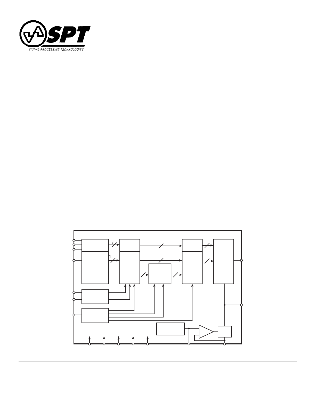
GENERAL DESCRIPTION
The SPT5220 is a monolithic 10-bit, 80 MWPS CMOS D/A
converter for high-resolution color graphics and video
system applications. The device operates from a single
+5 V power supply and all digital inputs are TTL/CMOS
compatible.
The SPT5220 generates RS343A-compatible video outputs
(capable of driving a doubly-terminated 75 Ω load) and
BLOCK DIAGRAM
APPLICATIONS
• High Resolution Color Graphics
• Medical Electronics: CAT, PET, MR Imaging Displays
• CAD/CAE Workstations
• General Purpose High-Speed D/A Conversion
• Direct Digital Synthesis (DDS)
• Digital Radio Transmitters/Modulators
• High Definition Television (HDTV)
RS170-compatible video outputs (capable of driving a singlyterminated 75 Ω load) without the need for external buffers.
The data latches minimize the data time skew and reduce the
glitches that can adversely affect many applications.
The device is available in a 28-lead plastic DIP package over
the commercial temperature range.
Sync
Blank
Bright
DØ-D9
N2C
Inverse
Clock
3
Digital
Input
Buffer
Code
Clock
Generator
DVDDDVSSV
10
BB
First
Latch
AVDDAV
3
5
5 31
Decoder
BGR
SS
Second
Latch
V
REF
36
Amp
3
DAC
CM
R
SET
Signal Processing Technologies, Inc.
4755 Forge Road, Colorado Springs, Colorado 80907, USA
Phone: (719) 528-2300 FAX: (719) 528-2370
I
OUT
Comp
Page 2

ABSOLUTE MAXIMUM RATINGS (Beyond which damage may occur)
1,2,3
Supply Voltages
ESD Susceptibility ..............................................±2,000 V
AVDD.......................................................... -0.5 to +7.0 V
DVDD......................................................... -0.5 to +7.0 V
Temperature
Operating Temperature Range (Ambient) .....0 to +70 °C
Input Voltages
Storage Temperature................................-55 to +150 °C
Any Digital Pin .................... DVSS-3.0 V to DVDD+3.0 V
Notes: 1. Operation at any absolute maximum rating is not implied. See Electrical Specifications for proper nominal
applied conditions in typical applications.
2. Absolute maximum ratings are limiting values applied individually while all other parameters are within
specified operating conditions. Functional operation under any of these conditions is not implied.
3. Applied voltage must be current limited to the specified range.
ELECTRICAL SPECIFICATIONS
TA=T
PARAMETERS CONDITIONS LEVEL MIN TYP MAX UNITS
DC CHARACTERISTICS
Resolution 10 Bits
Differential Linearity Error VI ±0.4 ±1.0 LSB
Integral Linearity Error VI ±0.6 ±1.0 LSB
Gray Scale Error VI ±5.0 % Gray
Monotonicity VI Guaranteed
Digital Input High Current V
Digital Input Low Current V
Digitial Input Capacitance fIN=1 MHz IV 20 40 pF
Analog Outputs
Internal Reference Voltage VI 1.16 1.235 1.36 V
Power Supply Rejection Ratio fIN=1 kHz, comp=0.1 µF V -30 dB
Operating Supply Voltage VI 4.75 5.00 5.25 V
Digital Input Voltage High VI 2.0 V
Effective Output Load V 37.5 Ω
Data Input Setup Time IV 2.0 ns
Data Input Hold Time IV 2.0 ns
Clock Cycle Time IV 12.5 ns
Clock Pulse Width High IV 5 ns
Clock Pulse Width Low IV 5 ns
to T
MIN
Gray Scale Current VI 22 mA
Output Current
Output Compliance VI -1.0 +1.5 V
Output Impedence V 11 kΩ
Output Capacitance fIN=1 MHz IV 14 30 pF
, AVDD=DVDD=VBB=+5.0 V, AVSS=DVSS=0.0 V, V
MAX
4
=1.235 V, R
REF
TEST TEST SPT5220
=2.4 V VI 1.0 µA
IN
=0.4 V VI -1.0 µA
IN
Bright to White VI 1.0 1.90 3.0 mA
White to Black VI 18.1 19.05 20.0 mA
Black to Blank VI 0.5 1.43 2.5 mA
Blank to Sync VI 6.5 7.62 8.5 mA
Sync Level VI 0 5 50 µA
LSB Size V 18.62 µA
Low VI VSS-0.3 0.8 V
=165 Ω, unless otherwise specified.
SET
DD
+0.3 V
Note: 4. To avoid power latch-up, drive all supply pins (AVDD, DVDD, and VBB) from the same source.
SPT
2 12/30/98
SPT5220
Page 3
ELECTRICAL SPECIFICATIONS
TA=T
PARAMETERS CONDITIONS LEVEL MIN TYP MAX UNITS
AC CHARACTERISTICS
Clock Rate 80 MWPS
Analog Output Delay V 7 ns
Analog Output Rise Time V 4 ns
Analog Output Fall Time V 4 ns
Analog Output Settling Time
Clock and Data Feedthrough
Glitch Impulse
Differential Gain Error V 0.8 %
Differential Phase Error V 0.9 Degree
Pipeline Delay (Clock Latency) IV 1 Clock Cycles
VDD Supply Current
to T
MIN
to ±1 LSB IV 100 150 ns
to ±2 LSB IV 70 100 ns
, AVDD=DVDD=VBB=+5.0 V, AVSS=DVSS=0.0 V, V
MAX
TEST TEST SPT5220
5
5
5
6
=1.235 V, R
REF
V -34 dB
IV 30 pv-sec
VI 50 70 mA
=165 Ω, unless otherwise specified.
SET
Note: 5. Clock and data feedthrough are functions of the amount of overshoot and undershoot on the digital inputs.
For this test, the digital inputs have a 1 kΩ resistor to ground driven by 74HC logic. Settling time does not
include clock and data feedthrough. Glitch impulse includes clock and data feedthrough.
6. At f
, IDD (typ) at AVDD=DVDD=5.25 V, CLK=0 V to 3 V (80 MWPS), NC2=High, Data (DØ-D9)=0 V to 3 V
MAX
(40 MWPS), Inverse=Sync=Blank=Bright=Low.
TEST LEVEL CODES
All electrical characteristics are subject to the
following conditions:
All parameters having min/max specifications
are guaranteed. The Test Level column indicates the specific device testing actually performed during production and Quality Assurance inspection. Any blank section in the data
column indicates that the specification is not
tested at the specified condition.
TEST LEVEL
I
II
III
IV
V
VI
TEST PROCEDURE
100% production tested at the specified temperature.
100% production tested at TA=+25 °C, and sample
tested at the specified temperatures.
QA sample tested only at the specified temperatures.
Parameter is guaranteed (but not tested) by design
and characterization data.
Parameter is a typical value for information purposes
only.
100% production tested at TA = 25 °C. Parameter is
guaranteed over specified temperature range.
SPT
SPT5220
3 12/30/98
Page 4

CIRCUIT DESCRIPTION AND OPERATION
CLOCK INPUT
The SPT5220 contains a 10-bit DAC, input buffers and
latches, internally or externally generated voltage reference and complete video controls. The following describes
the main operation of the device and outlines several
considerations that should be noted to achieve the best
performance.
Figure 1: Timing Waveform
7,8,9
t
PWH
t
CLK
t
PWL
CLK is the device clock input and is typically the pixel clock rate
of the system. It is TTL compatible. The digital data D0-D9 and
all video controls (SYNC, BLANK, BRIGHT) are all latched on
the rising edge of CLK. See figure 1.
CLK
DØ~D9
Output
Note: 7. Output delay (td) is measured from the 50% point of the rising edge of CLK to the full scale transition.
8. Settling time (t
LSB.
9. Output rise/fall time (tr, tf ) is measured between the 10% and 90% points of full scale transition.
N-1 Data N+1
t
S
t
H
t
D
t
SET
Pipeline Delay
) is measured from the 50% point of full scale transition to the output remaining within ±1, ±2
set
DIGITAL INPUTS AND VIDEO CONTROLS
All ten bits of data (D0-D9, D0 is the LSB) are latched into
the device on the rising edge of each clock cycle. There are
also three video control inputs to generate composite
video outputs. They are SYNC, BLANK and BRIGHT.
Table I - Video Output Truth Table
Sync Blank Bright Data (D9-D0) I
1 X X X 0 0 -40 Sync Level
0 1 X X 7.62 0.286 0 Blank Level
0 0 0 000… 9.05 0.340 7.5 Black Level
0 0 0 111… 28.10 1.054 100 White Level
0 0 1 000… 10.95 0.410 17.5 Enhanced Black Level
0 0 1 111… 30.00 1.125 110 Enhanced White Level
Note: 10. Double-terminated load of 75 Ω. VREF=1.235 V R
OUT
A logic 1 on the SYNC input generates the sync level. A logic 1
on the BLANK input generates the pedestal level. BRIGHT is the
bright signal input. These inputs are pipelined to maintain
synchronization with the digital input data. These video controls
produce the output levels needed to be compatible with video
system standards. Table I shows the video control effects on the
analog output.
(mA) V
SET
(V) Out (IRE) Description
OUT
=165 Ω. Inverse = 0. N2C = 1.
SPT
SPT5220
4 12/30/98
Page 5

There are two different input data formats available: binary
and two’s complement. In addition, these formats can be
either normal or inverted. The video control truth table for
these options are given in table II.
Table II - Video Control Truth Table
11
N2C INVERSE DATA (D9-D0) OUTPUT (I/O) DESCRIPTION
1 0 0000000000 Black Level Binary
1111111111 White Level
1 1 0000000000 White Level Inverse Binary
1111111111 Black Level
0 0 1000000000 Black Level Two's Complement
0111111111 White Level
0 1 1000000000 White Level Inverse Two's Complement
0111111111 Black Level
Note: 11. Doubly-terminated load of 75 Ω, Sync=Blank=Bright=Low
REFERENCE
The SPT5220 can be used with either an internal or external
voltage reference. The typical interface circuits are shown in
figures 2 and 3. When using an external reference (figure 2),
bypass capacitor. The COMP capacitor should be kept as
close as possible to the device to keep the lead lengths to an
absolute minimum.
the input voltage supplied must be 1.235 volt (typ). When
using the internal reference (figure 3), the V
pin should
REF
not drive any external circuitry except for the decoupling
capacitor. A bypass capacitor of 0.1 µF with the shortest
possible lead lengths should be connected between V
REF
and VSS. With either configuration, the COMP pin (compensation capacitor) should be connected to VDD through the
Rset is the full scale adjust control. A resistor (Rset) con-
nected between this pin and ground controls the magnitude
of the full-scale video signal. The value for Rset is determined
by the relationship:
Rset=4.1 x V
REF/IOUT
The electrical specifications are given with an Rset value of
165 ohms.
.
Figure 2 - Typical Interface Circuit (External Reference)
L1
+
C3
Driving Logic
Sync
Blank
Bright
D0 ~ D9
(LSB) (MSB)
N2C
Inverse
CLK
DV
DD
C1
DD
V
BB
DV
SPT5220
DV
SS
L3
L2
AV
DD
V
REF
I
OUT
COMP
R
set
AV
SS
C2
+
C4 C5
R
set
C6
R1
R2
Z
1
V
DD
To Video
Connector
V
SS
Component Description
C1, C2 10 µF Capacitor
C3 - C6 0.1 µF Ceramic
Capacitor
L1, L2, L3 Ferrite Bead
R1 75 Ω 1% Metal
Film Resistor
R2 1 kΩ 5% Resistor
R
SET
165 Ω 1% Film Resistor
(180 Ω//2 kΩ)
Z
1
1.235 V Voltage Reference
(ICL8069CCSQ2)
SPT
SPT5220
5 12/30/98
Page 6

Figure 3 - Typical Interface Circuit (Internal Reference)
L1
+
L3
C3
DV
DV
DD
SS
V
BB
SPT5220
L2
AV
DD
V
REF
I
out
COMP
R
set
AV
SS
C2
+
C4 C5
R
SET
C1
Driving Logic
Sync
Blank
Bright
D0 ~ D9
(LSB) (MSB)
N2C
Inverse
CLK
DV
DD
Note 12: AVDD, DVDD and VRB must be supplied from the same source (Analog +5 V)
to prevent a latch-up condition due to power supply sequencing.
Note 13: For applications requiring minimal signal distortion, use of the external
reference is recommended.
R1
C6
V
DD
T o Video
Connector
V
SS
Component Description
C1, C2 10 µF Capacitor
C3 - C6 0.1 µF Ceramic
Capacitor
L1, L2, L3 Ferrite Bead
R1 75 Ω 1% Metal
Film Resistor
R
SET
165 Ω 1% Film
Resistor (180 Ω//2 kΩ)
ANALOG OUTPUT
The SPT5220 generates RS-343A compatible video outputs
capable of directly driving a doubly-terminated 75 ohm load,
and RS-170 compatible video outputs capable of directly
Figure 4 - Composite Video Output Wave Form
LEVEL mA V
Bright
30.00
1.125
White
28.10
1.054
Black 9.05 0.340
Blank 7.62 0.286
14
10 IRE
100 IRE
7.5 IRE
driving a singly-terminated 75 ohm load without the need for
external buffers. Figure 4 shows the video waveforms associated with the output driving the doubly-terminated 75 ohm
load.
Sync 0.00 0.00
Note: 14. Doubly-terminated load of 75 Ω, V
SPT
40 IRE
=1.235 V, R
REF
=165 Ω. RS-343 levels and tolerances are assumed on all levels.
SET
6 12/30/98
SPT5220
Page 7

PC BOARD CONSIDERATIONS
DIGITAL SIGNAL INTERCONNECT
LAYOUT CONSIDERATIONS
To minimize noise on the power lines and ground lines, shield
and decouple the digital inputs. Keep the trace length between groups of VDD (AVDD, DVDD) and V
(AVSS, DVSS)
SS
as short as possible to minimize inductive ringing.
SUPPLY AND GROUND CONSIDERATIONS
Use a 0.1 µF ceramic capacitor in parallel with a 10 µF
tantalum capacitor for decoupling between the power line
and the ground line. The digital power plane (DVDD) and the
analog power plane (AVDD) are connected through a ferrite
bead. The digital ground plane (DVSS) and the analog
ground plane (AVSS) are also connected through a ferrite
bead. (See figures 3 and 4). Locate these ferrite beads within
three inches of the SPT5220.
The PCB line between the TTL driver (that drives the SPT5220)
and the input to the SPT5220 will have a low impedance
source and be terminated with a high impedance. It behaves
like a low impedance transmission line so signal transitions
will be reflected from the high impedance input of the SPT5220.
To reduce ringing caused by transmission line mismatch,
shorten the line length or terminate the line. Both serial and
parallel termination methods will work, but serial is preferred.
Serial termination is achieved by installing a resistor of
approximately 50 Ω between the TTL driver output and the
SPT5220 digital input.
ANALOG SIGNAL INTERCONNECT
To minimize noise pickup and reflections due to impedance
mismatch, locate the SPT5220 as closely as possible to the
output connector. The line between the DAC output and the
monitor input should be regarded as a transmission line since
it can cause problems in transmission line mismatch. Use the
double-termination method to avoid these problems. By
using the double terminated method, the transmission lines
are matched, providing an ideal, nonreflective system.
28-LEAD PLASTIC DIP (PDIP) PACKAGE OUTLINE
INCHES MILLIMETERS
K
28
I
1
J
A
B
SYMBOL MIN MAX MIN MAX
A 0.198 typ 5.08 typ
B 0.117 0.140 3.00 3.60
C 0.014 0.022 0.36 0.56
D 0.099 typ 2.54 typ
E 0.055 0.063 1.42 1.62
F 0.008 0.014 0.20 0.35
G 0.142 0.158 3.65 4.05
H 0.000 0.594 15.24
I 0.523 0.538 13.40 13.80
J 1.439 1.455 36.90 37.30
K 0 .080 typ 2.04 typ
L0° 15°
H
G
L
F
SPT
C
D
E
SPT5220
7 12/30/98
Page 8

PIN ASSIGNMENTS
DD
N/C
V
BB
DD
SS
D8
D7
D6
D5
D4
D3
D2
D1
1
2
3
4
5
6
7
8
9
10
11
12
13
14
AV
AV
AV
(MSB) D9
PDIP
28
27
26
25
24
23
22
21
20
19
18
17
16
15
COMP
R
SET
V
REF
N2C
I
OUT
AV
SS
INVERSE
CLK
DV
SS
DV
DD
BRIGHT
BLANK
SYNC
DØ (LSB)
PIN FUNCTIONS
Name Function
AV
DD
N/C No Connection
V
BB
AV
SS
D9 - D0 Digital Inputs (D9=MSB, D0=LSB)
SYNC Sync Signal Input (Logic 1 Generates Level)
BLANK Blank Signal Input (Logic 1 Generates Level)
BRIGHT Bright Signal Input
DV
DD
DV
SS
CLK Clock Input (TTL-Compatible)
INVERSE Inverse Signal Input
I
OUT
N2C Two's Complement Signal Input (Active Low)
V
REF
R
SET
COMP Compensation Capacitor
Analog Power
Substrate Power (Connected to AVDD)
Analog Ground
Digital Power
Digital Ground
Analog Current Output
Voltage Reference (Externally Driven)
Full-Scale Adjust Control
ORDERING INFORMATION
PART NUMBER TEMPERATURE RANGE PACKAGE TYPE
SPT5220SCN 0 to +70 °C 28L Plastic DIP
Signal Processing Technologies, Inc. reserves the right to change products and specifications without notice. Permission is hereby expressly
granted to copy this literature for informational purposes only. Copying this material for any other use is strictly prohibited.
WARNING - LIFE SUPPORT APPLICATIONS POLICY - SPT products should not be used within Life Support Systems without the specific
written consent of SPT. A Life Support System is a product or system intended to support or sustain life which, if it fails, can be reasonably
expected to result in significant personal injury or death.
Signal Processing Technologies believes that ultrasonic cleaning of its products may damage the wire bonding, leading to device
failure. It is therefore not recommended, and exposure of a device to such a process will void the product warranty.
SPT
SPT5220
8 12/30/98
 Loading...