

Page 1
SPT5216
16-BIT ULTRAHIGH SPEED DAC
Precision Thin Film
Resistor Network
1 kΩ
AA
AA
AA
AA
AA
AA
AA
AA
AA
AA
Switch
Bias
Network
gm
V
DD
(+5 V)
DGND
D15
(MSB)
D14
D0
(LSB)
10 V FSR
5 V FSR
VEE (-15 V)
DAC Out
DAC
RTN
Sense
DAC
RTN
1
DAC
RTN
2
Gain
Adj
Bandgap
V
REF
AGND
Ref
In
Gain
Adj
Ref
Out
2 kΩ
V
CC
(+15 V)
BPO
VEE (-15 V)
1 kΩ
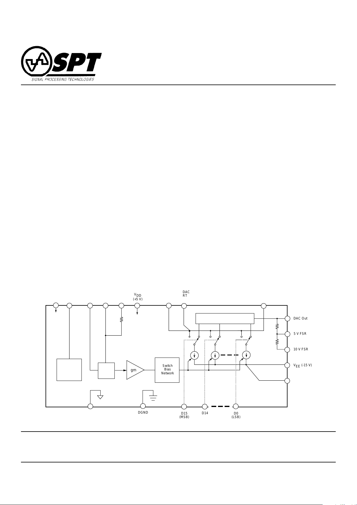
BLOCK DIAGRAM
GENERAL DESCRIPTION
The SPT5216 is a monolithic, high-performance, 16-bit digital-to-analog converter with unmatched speed and accuracy.
With its 150 nanosecond settling time, it is the highest speed
16-bit DAC in the industry. Unique features include the bandgap voltage reference and precision application resistors
which greatly simplify device application. Unlike other high
speed DACs, the SPT5216 can be used in either a currentoutput or voltage-output mode.
The internal application resistors support output range selections of 0 to +10, 0 to +5, -5 to +5, and -2.5 to +2.5 volts. These
internal resistors, used in conjunction with an external op
amp, provide current-to-voltage conversion. Because of the
high compliance voltage of the DAC output (±2.5 volts), the
SPT5216 can also provide a direct voltage drive into a high
impedance load without an external op amp.
The SPT5216 operates with ±15 volt analog supplies, a
separate +5 V digital supply and separate analog and digital
grounds to provide maximum noise immunity. All logic input
levels are TTL and 5 volt CMOS compatible. Laser-trimmed
thin film technology ensures accuracy over time and environmental changes.
The SPT5216 is available in 32-lead sidebrazed DIP and 44lead cerquad packages over the commercial temperature
range. It is also available in die form.
APPLICATIONS
• High Speed Analog-to-Digital Converters
• Automatic Test Equipment
• Digital Attenuators
• Digital Communication Equipment
• Waveform Generators
FEATURES
• Fast Settling Time - 150 nsec
• Excellent Linearity T. C. 1.5 ppm/°C
• On-Chip Band-Gap Voltage Reference
• On-Chip Application Resistors for Gain Selection
• TTL Compatible Inputs
Signal Processing Technologies, Inc.
4755 Forge Road, Colorado Springs, Colorado 80907, USA
Phone: (719) 528-2300 FAX: (719) 528-2370
Page 2

SPT
2 3/4/97
SPT5216
ELECTRICAL SPECIFICATIONS
TA = 0 to +70 °C, VCC = 15 V, VDD = 5 V, VEE = -15 V, unless otherwise specified. Minimum air flow is 50 LFPM.
TEST TEST SPT5216B SPT5216C
PARAMETER CONDITIONS LEVEL MIN TYP MAX MIN TYP MAX UNIT
ACCURACY SPECIFICATIONS
Integral Linearity Error VI ±.0015 ±.003 ±.0045 ±.006 %FSR
Integral Linearity Drift Drift V ±2.5 ±4.0 PPM/°C
Differential Linearity Error VI ±.003 ±.006 ±.009 ±.012 %FSR
Differential Linearity Drift Drift V ±2.5 ±4.0 PPM/°C
Gain Error VI ±.03 ±.5 ±.03 ±.5 %FSR
Gain Error Drift V ±20 ±20 PPM/°C
Unipolar Offset Error VI ±.02 ±.1 ±.02 ±.1 %FSR
Bipolar Offset Error VI ±2.5 ±25 ±2.5 ±25 mV
DAC OUTPUT SPECIFICATIONS
I
OUT
V5 5mA
R
OUT
V1 1kΩ
C
OUT
See Figure 1 V 12 12 pF
Output Compliance
2
V ±2.5 ±2.5 V
Output Noise BW = 1 MHz V 40 40 µV RMS
ABSOLUTE MAXIMUM RATING (Beyond which damage may occur) 25 °C (1)
Supply Voltages
VCC to AGND..........................................................+18 V
VEE to AGND .......................................................... -18 V
VDD to DGND ...........................................................+6 V
AGND to DGND Differential...................................+0.5 V
Input Voltages
All Digital Inputs to DGND ............-0.3 V to (VDD +0.3 V)
REF IN to AGND..............................................0 to +10 V
Temperature
Temperature, Ambient ..................................... 0 to 70 °C
case....................................-60 to +140 °C
junction.........................................+150 °C
Lead Temperature (soldering 10 seconds) .........+300 °C
Storage Temperature................................-65 to +100 °C
Note: 1. Operation at any Absolute Maximum Rating is not implied. See Electrical Specifications for proper nominal
applied conditions in typical applications.
Note 1: Operation at any Absolute Maximum Rating is not implied. See Electrical Specifications for proper nominal
applied conditions in typical applications.
Note 2: Accuracy is not guaranteed beyond this limit.
Page 3

SPT
3 3/4/97
SPT5216
ELECTRICAL SPECIFICATIONS
TA = 0 to +70 °C, VCC = 15 V, VDD = 5 V, VEE = -15 V, unless otherwise specified. Minimum air flow is 50 LFPM.
TEST TEST SPT5216B SPT5216C
PARAMETER CONDITIONS LEVEL MIN TYP MAX MIN TYP MAX UNIT
DYNAMIC SPECIFICATIONS
Settling Time to .0015% V 150 150 ns
LOGIC SPECIFICATIONS
V
IH
2 VI 4.5 4.5 V
VIL 2 VI 0.8 0.8 V
I
IH
VI 2 20 2 20 µA
I
IL
VI 2 20 2 20 µA
REFERENCE
Reference Output Voltage TA=25 °C I 4.99 5 5.01 4.99 5 5.01 V
Reference Output Voltage IV 4.98 5 5.02 4.98 5 5.02 V
Max. Reference Output Load3 Total Current V 8 8 mA
Output Noise4 BW = 1 MHz V 40 40 µV RMS
POWER SUPPLIES
VCC Supply IV 14.25 15.00 15.75 14.25 15.00 15.75 V
VEE Supply IV -14.25 -15.00 -15.75 -14.25 -15.00 -15.75 V
VDD Supply IV 4.75 5.00 5.25 4.75 5.00 5.25 V
VCC Supply Current VI 5 8 5 8 mA
VEE Supply Current VI 25 35 25 35 mA
VDD Supply Current VI 8 12 8 12 mA
Power Dissipation VI 490 705 490 705 mW
PSRR, V
CC
+15 V±5% V .001 .001 %G/%PS
PSRR, V
EE
-15 V±5% V .01 .01 %G/%PS
PSRR, V
DD
+5 V±5% V .001 .001 %G/%PS
Note 3: Reference Load: REF IN = 1 mA BPO = 2.5 mA
Note 4: Reference decoupled as shown in figure 6.
TEST PROCEDURE
100% production tested at the specified temperature.
100% production tested at TA=25 °C, and sample
tested at the specified temperatures.
QA sample tested only at the specified temperatures.
Parameter is guaranteed (but not tested) by design
and characterization data.
Parameter is a typical value for information purposes
only.
100% production tested at TA = 25 °C. Parameter is
guaranteed over specified temperature range.
TEST LEVEL
I
II
III
IV
V
VI
TEST LEVEL CODES
All electrical characteristics are subject to the
following conditions:
All parameters having min/max specifications
are guaranteed. The Test Level column indicates the specific device testing actually performed during production and Quality Assurance inspection. Any blank section in the data
column indicates that the specification is not
tested at the specified condition.
Page 4

SPT
4 3/4/97
SPT5216
TERMINOLOGY
INTEGRAL LINEARITY ERROR
Integral linearity error is a measure of the maximum deviation
from a straight line passing through the end points of the DAC
transfer function. It is measured after adjusting for zero offset
error and zero gain error.
DIFFERENTIAL LINEARITY ERROR
Differential linearity error is the difference between the measured change and the ideal 1 LSB change between two
adjacent codes. A specified differential nonlinearity of <1 LSB
ensures monotonicity and no missing codes.
OFFSET ERROR AND GAIN ERROR
Offset error is the absolute difference between actual and
theoretical output voltage at code all 1s.
Gain error is the difference between the measured and ideal
full scale output range (after offset has been adjusted to zero)
expressed as a percent of the ideal output level. The actual
full scale output contains both the gain error and the offset
error. Both offset and gain errors are adjustable to zero using
the external trim network shown in figures 4 and 5 respectively.
OUTPUT COMPLIANCE
Output compliance is the allowable range of voltage swing for
pin DAC OUT. Other specifications, such as integral
nonlinearity, are not guaranteed beyond the specified output
compliance voltage.
GENERAL CIRCUIT DESCRIPTION
The SPT5216 uses a unique design approach to set a new
standard in monolithic DAC performance. It delivers exceptional 16-bit accuracy and stability over temperature and, at
the same time, exhibits an extremely fast 150 ns settling time.
On chip support functions include a stable band-gap voltage
reference and application resistors for output scaling. Inclusion of these functions reduces the external analog component requirements and further increases accuracy. Digital
circuitry on the chip is kept to a minimum (limited to the digital
inputs), thus minimizing internal noise generation and providing interface flexibility.
DAC CIRCUITRY
The SPT5216 uses current source segmentation for the most
significant bits and an R-2R ladder for the least significant
bits. The ladder, which consists of a resistor network, succes-
sively divides the (remaining) reference current to produce a
binary weighted current division. In other words, in moving
down the ladder, each 2R resistor leg has half the current flow
of the previous leg. Each 2R resistor leg is connected to a
current source that is trimmed during manufacturing to provide the 16-bit accuracy. Bipolar switches within each leg are
controlled by the respective data bits (pins D0 through D15).
When the controlling data bit is low, the 2R resistor leg current
is steered to pin DAC OUT. When the data bit is high, the leg
current is steered to the DAC RTN pins (DAC RTN 1, and
DAC RTN 2), which are externally connected to analog
ground.
Figure 1 illustrates the equivalent output circuit of the SPT5216
showing on-chip application resistors and parasitic capacitances.
Figure 1 - Equivalent SPT5216 Output Circuit
10 V FSR
5 V FSR
DAC Out
DAC RTN
Sense
DAC
1 kΩ
1 kΩ
1 kΩ
0-5 mA
DAC RTN 1
DAC RTN 2
5 Ω
Substrate
8 pF
Substrate
8 pF
12 pF
Substrate
V
EE
AGND
APPLICATION INFORMATION
ACTIVE CURRENT-TO-VOLTAGE CONVERSION
In many DAC applications the output current needs to be
converted into a usable voltage signal. The most common
current-to-voltage configuration for the SPT5216 output is
shown in figure 2. Here, an external op amp in conjunction
with the internal feedback resistor(s) are used for current-tovoltage (I-to-V) conversion. The op amp provides both a
buffered V
OUT
and maintains DAC OUT at a virtual ground.
This way, V
OUT
can provide up to a 10 volt output swing
(using internal feedback resistors) and the output compliance
specification (±2.5 volts maximum) is met.
V
OUT
swing is determined by the feedback resistance. For a
5 volt V
OUT
swing, the op amp's output is connected to
pin 5 V FSR (Full Scale Range) which provides an internal
1kΩ feedback resistance. A 10 volt V
OUT
swing is derived by
connecting the op amp output to pin 10 V FSR. This feedback
connection option is illustrated by the dotted line in figure 2.
Page 5

SPT
5 3/4/97
SPT5216
Properly trimmed (as discussed later), the connections of
figure 2 as indicated, would result in the ideal output values
as listed in table I.
Figure 2 - Connection of External OP AMP for Active
Current-to-Voltage Conversion
10 V FSR
5 V FSR
DAC Out
DAC RTN
Sense
DAC
V
Out
Or
OP AMP
DAC RTN 1
DAC RTN 2
AGND
1 kΩ
1 kΩ
1 kΩ
0-5 mA
I-To-V Converter
REF Out
REF In BPO
Optional Bipolar Offset Connection
2 kΩ
+
-
Table I - Normalized Voltage Values for Programmable
Output Ranges (Using Figure 6)
0.00 V0.00 V
+ 76.3 µV
1111 1111 1111 1111
1111 1111 1111 1110
0111 1111 1111 1111
0000 0000 0000 0000
+ 152.6 µV
+ 5.00 V
+ 9.999846 V
10 VOLT
INPUT CODE
5 VOLT
+ 2.500 V
+4.999924 V
10 VOLT
- 5.00 V
0.00 V
+ 4.999846 V
- 4.999846 V
5 VOLT
- 2.50 V
- 2.499924 V
0.00 V
+2.499924 V
OUTPUT VOLTAGE RANGES
UNIPOLAR BIPOLAR
To configure the bipolar output range as indicated in table I,
connect the BPO pin to DAC OUT. This connection option is
illustrated in figure 2; this offsets the output range by half of
the full scale range so that a half-scale digital input value
results in a output current value of zero.
The pin connections for the active I-to-V ranges supported by
the internal application resistors are summarized in table II.
OPERATIONAL AMPLIFIER SELECTION
Selection of the external op amp involves understanding the
final system performance requirements in terms of both
speed and accuracy. To maintain the 16-bit accuracy provided by DAC OUT at V
OUT
shown in figure 2, the op amp
open loop gain (Avol) must be 96 dB minimum. Any gain
lower than this will contribute an error in the I-to-V conversion circuit. To maintain the 150 ns settling time capability
provided by DAC OUT at V
OUT
, the op amp must have a
minimum gain bandwidth of 50 MHz and settling time of
less than 100 ns to 0.0015% of full scale.
Table II - Device Pin Connection Summary for Output
Range Programming
(Active I-to-V Conversion Only)
Connected To
Op Amp Output
Not Connected
Not Connected
OUTPUT VOLTAGE RANGES
UNIPOLAR BIPOLAR
DEVICE PINS
5 Volt 10 Volt 5 Volt 10 Volt
10 V FSR
Not Connected Not Connected
Connected To
Op Amp Output
5 V FSR
Connected To
Op Amp Output
Connected To
Op Amp Output
Not Connected
BPO
Not Connected
Connected
To DAC Out
Connected
To DAC Out
PASSIVE CURRENT-TO-VOLTAGE CONVERSION
Because of the SPT5216's high voltage compliance, a voltage output can be derived directly at DAC OUT in a method
suitable for some applications. By driving a load resistor
directly with the current from DAC OUT, a voltage drop results
producing V
OUT
. An example of this implementation is shown
in figure 3, where an internal feedback resistor is used as the
load 10 V FSR is grounded to optimize settling time. By
utilizing all internal resistors, this circuit offers optimized
stability and matching.
Output current from the DAC ranges between 0 and 5 mA,
which corresponds to an input code of all 1s and all 0s,
respectively. For unipolar mode, the net 500 Ω load of figure
3 results in a -2.5 to 0 volt output range. For bipolar mode, the
output voltage range is from +1.67 V to -1.67 V (typical). Both
output ranges are within the specified output compliance
limits. An external load resistor could also be used with this
circuit, however, there are difficulties with this arrangement:
thermal tracking is not optimum, and the gain adjustment
required to overcome the absolute internal resistance and
DAC output current errors is beyond the correction range
provided by the trim circuit. This is described later.
Note that the input resistance of the circuit driven by V
OUT
will
be placed in parallel with the load resistor. This limits the
application of figure 3 to high impedance loads. Also note that
if a buffer (or other active circuit) is used at V
OUT
in figure 3,
that circuit's CMRR must be at least 100 dB to maintain the
DAC's accuracy. This is an advantage of the active currentto-voltage configuration shown in figure 2, where the input of
the op amp is always at virtual ground.
Page 6

SPT
6 3/4/97
SPT5216
Figure 3 -Connection of Internal Load Resistors for Passive
Unipolar/Bipolar Current-to-Voltage Conversion
LOGIC INTERFACE
Because of the low logic input current specification, most
high-speed CMOS logic families will adequately drive the
SPT5216. Nonadherence to the VIH specification will result in
a less than specified DAC accuracy. High-speed CMOS logic
(HC), high-speed CMOS logic with TTL-compatible outputs
(HCT) or TTL logic with open-collector outputs are directly
compatible with the SPT5216 logic inputs.
GAIN ADJUSTMENT
With the gain error of the SPT5216 pre-trimmed to within
±0.15% of full scale accuracy, many applications require
external gain adjustments. Configuration of the external gain
adjustment network is shown is figure 5. The adjustment
potentiometer is connected between two low noise voltage
sources, REF OUT and AGND, as shown. The two bypass
capacitors shown further help to eliminate noise. Because of
the voltage source asymmetry in relationship to the potentiometer wiper, the adjustment range is an asymmetric -0.6%
to +1%. This adjustment range does sufficiently compensate
for the error of the device, and the network will work for any
type of output configuration. The adjustment range can be
made larger and symmetrical by using a circuit similar to the
offset compensation network as shown in figure 4, but with
the consequence of introducing power supply noise (and
power supply variations) into the vital voltage reference
circuit.
The selection criteria for the gain adjustment network components is similar to those described for the offset compensation network. Accuracy is not as important as temperature
stability.
Figure 5 - Gain Trim Network Suitable for All Output
Configurations
5 Volt
Bandgap
Voltage
Reference
gm
AMP
Switch
Bias
Network
To DAC
Ref Out
10 kΩ
Ref In
AGND
Gain Adj
330 kΩ
Gain
Adj
Circuit
15 µF 0.01 µF
+
10 V FSR
5 V FSR
DAC Out
DAC RTN
Sense
DAC
V
OUT
DAC RTN 1
DAC RTN 2
1 kΩ
1 kΩ
1 kΩ
0-5 mA
(To High Impedance Load)
AGND
AA
AA
AA
AA
Leave Open For
Bipolar Mode
BPO
For Bipolar Mode Only
OUTPUT OFFSET COMPENSATION
Although the zero offset error of the SPT5216 is within ±0.1%
of the full scale range, some applications require better
accuracy. The offset trim network of figure 4 shown connected to DAC OUT allows offset adjustment in excess of
±0.2%. This trim network can be used for the active I-to-V
conversion network of figure 2 or the passive circuit of
figure 3. When using an external op amp as in figure 2,
optimum offset stability may be achieved by using the nulling
network recommended by the op amp's manufacturer.
Although accuracy of the offset network components is not
important, temperature tracking of the resistor and potentiometer values will affect offset trim stability. The resistors and
potentiometer should have a low temperature coefficient and
the potentiometer should be a high quality, multi-turn component to ensure minute adjustability and stability over time and
temperature. The 0.1 µF capacitors shown (typically ceramic) are used to decouple power supply noise from the
DAC output circuit.
Figure 4 - Offset Compensation
0.1 µF
10 V FSR
5 V FSR
DAC Out
DAC RTN
Sense
AGND AGND
0.1 µF
10 kΩ
-15 V+15 V
V
OUT
OP AMP
470 kΩ
DAC
10 kΩ10 kΩ
+
-
Page 7

SPT
7 3/4/97
SPT5216
Figure 6 - Typical SPT5216 Application Circuit
Bipolar
Offset
Connection
V
OUT
-15 V+15 V
10 kΩ
0.1 µF
10 kΩ
10 kΩ
0.1 µF
R-2R Ladder Network
1 kΩ
Bandgap
V
Ref
DGND
AGND
D15
(MSB)
D14
D0
(LSB)
10 V FSR
5 V FSR
DAC OUT
DAC
RTN
Sense
DAC
RTN 1
DAC
RTN 2
REF
IN
GAIN
ADJ
REF
OUT
2 kΩ
BPO
OP AMP
Data Input
10 kΩ
Optional Offset Trim Network
V
OUT
Range
Selection
Optional Gain Trim Network
SPT5216
470 kΩ
15 µF 0.01 µF
330 kΩ
R2
R1
VEEV
EE
V
CC
V
DD
.01 µF .01 µF
.01 µF
15 µF 15 µF 15 µF
V
EE
AGND
V
CC
DGND
V
DD
++ +
+
Switch
Bias
Network
gm
Gain
Adj
1 kΩ
+
-
OFFSET AND GAIN CALIBRATION PROCEDURE
This calibration procedure is only applied to the I-to-V applications as shown in figure 6.
The calibration consists of adjusting the V
OUT
most negative
voltage to its ideal value for the offset adjustment and
adjusting the most positive V
OUT
to its ideal value for gain
adjustment. The offset and gain errors listed in the specifications for both unipolar and bipolar operation may be adjusted
to zero using R1 and R2 (see figure 6) respectively. All
components in the optional offset trim network and optional
gain trim network shown in figure 6 should have a low
temperature coefficient. The potentiometers (R1 and R2)
should be multi-turn components to ensure minute
adjustability.
If the adjustment is not needed, remove the optional offset
trim network from the circuit.
Unipolar
The first step is offset adjustment. Set the input code to 1111
1111 1111 1111 and adjust R1 until V
OUT
reads zero volts for
either 5 V FSR operation or 10 V FSR operation.
Next is the gain adjustment. Set the input code to 0000 0000
0000 0000 and adjust R2 until V
OUT
reads +4.999924 volts
for 5 V FSR operation or +9.999846 volts for 10 V FSR
operation.
Bipolar
For the Bipolar mode of operation, start the calibration by
adjusting the offset. Set the input code to 1111 1111 1111
1111 and adjust R1 until V
OUT
reads -2.50000 volts for 5 V
FSR or -5.00000 volts for 10 V FSR operation. The gain error
calibration is done by setting the input code to 0000 0000
0000 0000 and adjusting R2 until V
OUT
reads +2.499924 V
for 5 V FSR operation or +4.999848 volts for 10 V FSR
operation.
Page 8

SPT
8 3/4/97
SPT5216
CIRCUIT LAYOUT CONSIDERATIONS
In any analog system design, care must be taken in the
circuit layout process. The design of a high-speed, 16-bit
analog system offers an exceptional challenge. The integrity
of the system's power supply and grounding is critical and,
as with any precision analog component, good decoupling is
needed directly at the device. Analog signal traces must be
routed in a manner to minimize coupling from potential noise
sources. With a 5 volt full-scale output voltage range, a mere
38 µVp-p noise level is equivalent to 1/2 LSB. Low amplitude
noise such as this is virtually impossible to eliminate without
totally shielding the analog circuit portion.
The power supply must be a well-regulated, noise-free analog voltage source. As with any analog device, the PSRR
performance of the SPT5216 degrades with higher frequency
components. Logic noise in the supply or ground line contains
high frequency components, so separate supplies and ground
returns are recommended for the analog and logic portions of
the system. Radiated noise from digital signal traces and
power supply traces must also be avoided. Completely shield
the analog circuit portion from digital circuitry and digital
power supplies and ground. A separate analog ground plane
near the device should be used to shield the digital data lines
going into the device; this plane should have a trace that
completely surrounds the digital inputs, if possible. If an
analog ground plane is used with the device for shielding,
keep the space between the digital ground plane and analog
ground plane wide to prevent capacitive coupling. The best
analog ground plane is one with the least resistance, i.e., the
minimum total "squares" of surface area, regardless of size.
All device grounding should be to the analog ground plane,
except for the GND RTN pins which should be tied to the
plane at one connection point only.
Figure 6 shows the implementation of decoupling devices
(0.01 µF and 15 µF in parallel) at pin REF OUT. These
devices should be connected to the analog ground and their
incorporation will minimize the overall D/A conversion noise.
Since virtually all the interfacing to the SPT5216 is analog in
nature (the logic inputs are actually analog current switches),
DGND and AGND should be tied together at the device and
treated as an analog ground. This analog ground and the
system's digital ground should be inter-tied only at a single
point which has a low impedance path back to the system's
power supplies. This will prevent modulation of the analog
ground by digital power supply currents as well as digital
noise injection.
The external components should be connected to the
SPT5216 with minimum length leads to help prevent noise
coupling. The inputs of the external op amp are especially
sensitive, so they should have short traces and be well
shielded.
To the circuit driven by the SPT5216, a voltage drop in the
common analog ground will appear as a voltage offset. To
avoid this, the SPT5216 includes a DAC SENSE pin which
can be used for remote ground potential sensing.
LONG-TERM STABILITY VERSUS TEMPERATURE
As with all high speed, high resolution digital-to-analog
converters, the initial accuracy of the device will degrade
with both time and temperature. The graph shown in figure
7 can be used to determine the expected change in linearity
performance over time when the device is operated at
various ambient temperatures. This graph shows how long
it will take for the SPT5216 linearity to change by 8 ppm (or
1/2 LSB) at any operating temperature. The curve shown is
valid for both integral nonlinearity (ILE) and differential
nonlinearity (DLE) changes.
Figure 7 - Linearity Performance over Time
0 20 40 60 80 100 120 140
10
2
10
3
10
4
10
5
10
6
10
7
10
8
1 month
1 year
100 years
1000 years
Time (Hours)
Temperature (°C)
Nonlinearity vs. Time/Temperature
Expected time required to produce an 8 ppm (1/2 LSB)
linearity (ILE or DLE) shift as a function of temperature.
Page 9

SPT
9 3/4/97
SPT5216
PACKAGE OUTLINES
32-Lead Sidebrazed
A
B
C
D
E
F
G
1
32
I
H
J
44-Lead Cerquad
C
D
A B
A
B
0 - 5°
E
F
G
H
I
I
INCHES MILLIMETERS
SYMBOL MIN MAX MIN MAX
A 0.081 0.099 2.06 2.51
B 0.016 0.020 0.41 0.51
C 0.095 0.105 2.41 2.67
D .050 typ 1.27
E 0.040 1.02
F 0.175 0.225 4.45 5.72
G 1.580 1.620 40.13 41.15
H 0.585 0.605 14.86 15.37
I 0.009 0.012 0.23 0.30
J 0.600 0.620 15.24 15.75
INCHES MILLIMETERS
SYMBOL MIN MAX MIN MAX
A 0.550 typ 13.97 typ
B 0.685 0.709 17.40 18.00
C 0.037 0.041 0.94 1.04
D 0.016 typ 0.41 typ
E 0.008 typ 0.20 typ
F 0.027 0.051 0.69 1.30
G 0.006 typ 0.15 typ
H 0.080 0.150 2.03 3.81
I 0.040 typ 1.02 typ
Page 10

SPT
10 3/4/97
SPT5216
ORDERING INFORMATION
PRODUCT TEMPERATURE
NUMBER RANGE PACKAGE
SPT5216BCJ 0 to +70 °C 32-Lead Sidebrazed
SPT5216CCJ 0 to +70 °C 32-Lead Sidebrazed
SPT5126BCQ 0 to +70 °C 44-Lead Cerquad
SPT5126CCQ 0 to +70 °C 44-Lead Cerquad
SPT5216CCU +25 °C Die*
*Please see the die specification for guaranteed electrical performance.
PIN FUNCTIONS
NAME FUNCTION
5 V FSR Output range scaling application resistor
10 V FSR Output range scaling application resistor
V
DD
+5 volt power supply connection
DGND Digital ground connection
V
CC
+15 volt power supply connection
DAC OUT Analog current output of DAC
DAC RTN 1 DAC ground current return path
V
EE
-15 volt power supply connection
AGND Analog ground connection
Gain ADJ Input reference trim adjustment
REF IN Input for internal or external reference
REF OUT Output of internal reference
BPO Output offsetting application resistor
V
EE
-15 volt power supply connection
DAC RTN 2 DAC ground current return path
DAC RTN DAC ground current sense connection
Sense
D0 Input data bit 0 (LSB)
D1-14 Input data bit 1-14
D15 Input data bit 15 (MSB)
PIN ASSIGNMENTS
32
31
30
29
28
27
26
25
24
23
22
21
20
19
18
17
D15 (MSB)
D12
D10
D9
D8
D14
D13
D11
D7
D4
D2
D1
D0 (LSB)
D6
D5
D3
1
2
3
4
5
6
7
8
9
10
11
12
13
14
15
16
5 V FSR
DGND
DAC OUT
DAC RTN 1
10 V FSR
V
DD
V
CC
V
EE
REF IN
BPO
V
EE
DAC RTN
SENSE
AGND
Gain ADJ
REF OUT
DAC RTN 2
1
2
3
4
5
6
7
8
9
10
1
1
D4
D5
D6
D7
D8
D9
D10
D11
D12
D13
D14
33
27
23
32
31
30
29
28
26
25
24
V
CC
DGND
V
DD
5 V SFR
D15
N/C
N/C
N/C
N/C
N/C
10 V SFR
22
21
20
19
18
17
16
15
14
13
12
34
35
36
38
37
39
40
41
42
43
44
BPO
Ref Out
Ref In
Gain Adj
AGND
V
EE
DAC RTN1
DAC Out
N/C
N/C
V
EE
DAC RTN 2
RTN Sense
D0
D1
D2
D3
N/C
N/C
N/C
N/C
N/C
DIP
Cerquad
Signal Processing Technologies, Inc. reserves the right to change products and specifications without notice. Permission is hereby expressly
granted to copy this literature for informational purposes only. Copying this material for any other use is strictly prohibited.
WARNING - LIFE SUPPORT APPLICATIONS POLICY - SPT products should not be used within Life Support Systems without the specific
written consent of SPT. A Life Support System is a product or system intended to support or sustain life which, if it fails, can be reasonably
expected to result in significant personal injury or death.
Signal Processing Technologies believes that ultrasonic cleaning of its products may damage the wire bonding, leading to device
failure. It is therefore not recommended, and exposure of a device to such a process will void the product warranty.
 Loading...