

Page 1
SPT5110
8-BIT, 30 MWPS TRIPLE VIDEO DAC
FEATURES
• 8-Bit Triple Video Digital-to-Analog Converter
• 30 MWPS Operation (typ)
• Low Power: 135 mW
• Internal Voltage Reference
• 5 V Monolithic CMOS
• 48-Pin QFP Package (7 mm x 7 mm, 0.5 mm Pitch)
Current
Switch
Cell
Array
(Cell 4)
Current
Switch Cell
Array (Cell 63)
Latch
Decoder
Latch
AV
DD
I
OR
(LSB) DRØ
DR1
DR2
DR3
DR4
DR5
DR6
(MSB) DR7
CLKR
V
CS
V
REF
Current
Switch Cell
Array (Cell 63)
Latch
Decoder
Latch
I
OB
(LSB) DBØ
DB1
DB2
DB3
DB4
DB5
DB6
(MSB) DB7
CLKB
Current
Switch Cell
Array (Cell 63)
Latch
Decoder
Latch
R
OUT
B
OUT
G
OUT
I
OG
(LSB) DGØ
DG1
DG2
DG3
DG4
DG5
DG6
(MSB) DG7
CLKG
V
CS
V
REF
AV
DD
AV
DD
Current
Switch
Cell
Array
(Cell 4)
Current
Switch
Cell
Array
(Cell 4)
AV
DD
AV
DD
AV
SS
AV
DD
AV
DD
AV
SS
AV
SS
AV
DD
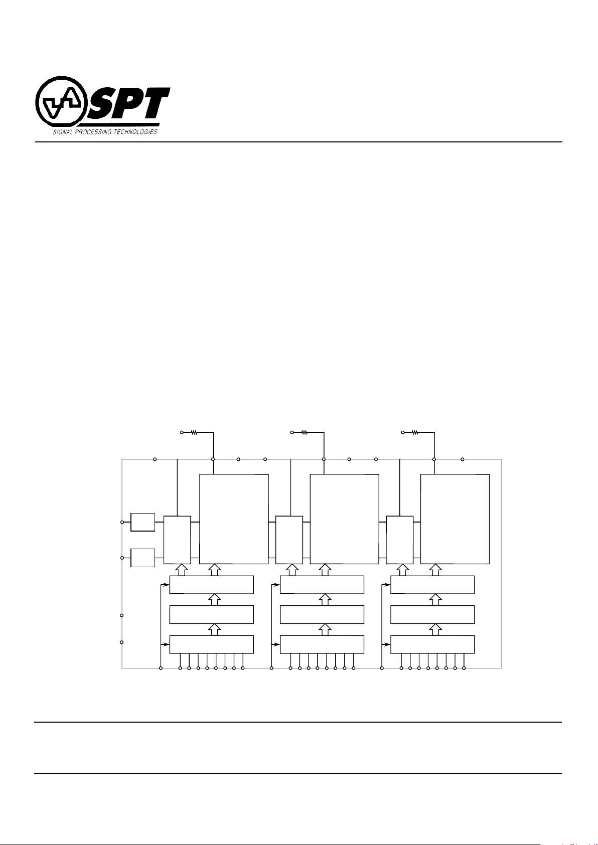
GENERAL DESCRIPTION
The SPT5110 is an 8-bit, 30 MWPS triple video digital-toanalog converter specifically designed for high performance,
high resolution color graphics monitor and video processing
applications. A single external resistor controls the fullscale output current. The differential linearity errors of the
DACs are guaranteed to be a maximum of ±0.5 LSB over the
full temperature range. The device is available in a 48-lead
QFP package in the commercial temperature range.
APPLICATIONS
• Desktop Video Processing of S-Video and CCIR-601
Video Signals
• VGA Color Graphics Monitors
• Professional Video Equipment
• Digital Television
Signal Processing Technologies, Inc.
4755 Forge Road, Colorado Springs, Colorado 80907, USA
Phone: (719) 528-2300 FAX: (719) 528-2370
BLOCK DIAGRAM
Page 2

SPT
2 3/14/97
SPT5110
ELECTRICAL SPECIFICATIONS
f
CLK
= 27 MWPS, AVDD = 5.0 V, Output Pull-Up Load = 240 Ω, TA = 25 °C, AVSS = 0.0 V, unless otherwise specified.
TEST TEST
PARAMETERS CONDITIONS LEVEL MIN TYP MAX UNITS
DC ELECTRICAL CHARACTERISTICS
DC Performance
Resolution 8.0 Bits
Differential Linearity I ±0.25 ±0.3 LSB
Differential Linearity T
A
= T
MIN
to T
MAX
I ±0.5 LSB
Integral Linearity I ±0.5 ±1.0 LSB
Analog Outputs
Output Voltage Range V
CS
= +1.27 V I 3.6 5.0 V
Conversion Rate I 27 30 MWPS
Output Offset Voltage I 17 25 mV
Signal-to-Noise Ratio I 41 47 dB
Differential Phase V 1 Degrees
Differential Gain V 2 %
Glitch Energy V 100 pV-s
Settling Time I 31 27 ns
Propagation Delay (t
pd
) V 10 12 ns
Crosstalk I -47 dB
FS Control Voltage (VCS) V 1.0 1.4 V
Digital Inputs and Timing
Input Current, Logic High VIH = 5 V I 5 µA
Logic Low V
IL
= 0 V I -5 µA
Set-Up Time, Data and Controls (t
S
)I5 ns
Hold Time, Data and Controls (t
h
) I 10 ns
Clock Pulse Width (Low) I 18.5 ns
Clock Pulse Width (High) I 18.5 ns
Power Supply Requirements
Supply Voltage I 4.75 5.25 V
Supply Current I 27 mA
Power Dissipation I 135 mW
ABSOLUTE MAXIMUM RATING (Beyond which damage may occur)
1
Supply Voltages
AV
DD
(measured to AVSS)........................... -0.3 to 7.0 V
Input Voltage
Clock and Data .........................................AVSS to AV
DD
Output Current
I
OUT
.............................................................................
0 to 7 mA
Temperature
Operating, ambient ........................................0 to +70 °C
Storage .....................................................-55 to +125 °C
Note: 1. Operation at any Absolute Maximum Ratings is not implied. See Electrical Specifications for proper nominal applied
conditions in typical applications.
Page 3

SPT
3 3/14/97
SPT5110
CURRENT OUTPUTS
Each red, green and blue current output should have a load
resistor connected to AVDD. The resistors are typically 240 Ω
and should be kept in the 150 Ω to 250 Ω range.
Table I - Binary Codes
1 LSB = 5.49 mV, VCS = 1.27 V
Digital Input Analog
Step A7 A6 A5 A4 A3 A2 A1 A0 Out (V)
(MSB) (LSB)
0 000000003.6000
1 000000013.6055
2 000000103.6110
3 000000113.6165
. . .
. . .
. . .
254 111111104.9890
255 111111114.9945
INTERFACE CONSIDERATIONS
Figure 1 shows a typical interface circuit of the SPT5110 in
normal circuit operation.
SUPPLY AND GROUND CONSIDERATIONS
SPT suggests that all power supply pins (AVDD) be tied
together and decoupled using a 0.1 µF ceramic capacitor in
parallel with a 10 µF tantalum capacitor.
INTERNAL REFERENCE VOLTAGE (V
REF
)
Voltage reference is internally generated. Connect a 0.1 µF
bypass capacitor as close to the pin as possible.
FULL-SCALE ADJUST CONTROL (VCS)
Connect a 0.1 µF bypass capacitor with the shortest possible
lead length between VCS and AVSS. A resistor connected
between this pin and AVDD controls the magnitude of the fullscale video signal.
The output voltage range of the SPT5110 can be kept
constant and stable by keeping the value of VCS to ground
constant. The full-scale voltage changes according to VCS.
(See figure 2.)
TEST LEVEL CODES
All electrical characteristics are subject to the
following conditions: All parameters having min/
max specifications are guaranteed. The Test
Level column indicates the specific device testing actually performed during production and
Quality Assurance inspection. Any blank section in the data column indicates that the specification is not tested at the specified condition.
TEST LEVEL
I
II
III
IV
V
VI
TEST PROCEDURE
100% production tested at the specified temperature.
100% production tested at TA=25 °C, and sample
tested at the specified temperatures.
QA sample tested only at the specified temperatures.
Parameter is guaranteed (but not tested) by design
and characterization data.
Parameter is a typical value for information purposes
only.
100% production tested at TA = 25 °C. Parameter is
guaranteed over specified temperature range.
Page 4

SPT
4 3/14/97
SPT5110
Figure 3 - Timing Diagram
Figure 2 - Typical Performance Characteristics
Figure 1 - Typical Interface Circuit
t
h
N-Data
t
s
1/2 LSB
t
pd
N-Output Level
1/2 LSB
Full Scale Output Voltage
VCS (V)
1.41.31.21.11.00.9
2.5
3.0
3.5
4.0
4.5
5.0
Full Scale Output Voltage
vs VCS
Load Resistors = 240 Ω
Ta = +25 °C
Digital Inputs = All Ø
10 kΩ
5 kΩ
2 kΩ
AV
DD
SPT5110
V
REF
AV
SS
AV
DD
AV
SS
B
OUT
AV
SS
G
OUT
AV
SS
R
OUT
AV
SS
AV
DD
AV
DD
AV
SS
N/C
(MSB) R7
R6
R5
R4
AV
SS
R3
R2
R1
(LSB) RØ
N/C
0.1 µF
+5 V
0.1 µF
CLOCK
+5 V
B4
B5
B6
B7 (MSB)
GØ (LSB)
G1
G2
G3
G4
G5
G6
G7 (MSB)
12
1
1
10
9
8
7
6
5
4
3
2
1
V
CS
AV
SS
AV
DD
AV
DD
AV
SS
CLK
R
CLK
G
CLK
B
BØ (LSB)
B1
B2
B3
24
23
22
21
20
19
18
17
16
15
14
13
25
26
27
28
29
30
31
32
33
34
35
36
37
38
39
40
41
42
43
44
45
46
47
48
10 µF
+
-
100 Ω
100 Ω
100 Ω
+5 V
AV
DD
0.1 µF
240 Ω
240 Ω
240 Ω
+5 V
0.1 µF
0.1 µF
0.1 µF
Page 5

SPT
5 3/14/97
SPT5110
PACKAGE OUTLINE
48-Lead QFP
Index
Pin 1
A
B
C
D
E F
G
I
H
J
K
L
INCHES MILLIMETERS
SYMBOL MIN MAX M IN MAX
A 0.343 0.359 8.79 9.21
B 0.269 0.277 6.89 7.11
C 0.269 0.277 6.89 7.11
D 0.343 0.359 8.79 9.21
E 0.016 0.023 0.41 0.59
F 0.004 0.012 0.09 0.31
G 0.052 0.067 1.34 1.71
H 0.000 0.006 0.16
I 0.003 0.007 0.074 0.176
J 0.011 0.028 0.29 0.71
K 0.039 typ 1.0 typ
L0°10° 0° 10°
Page 6

SPT
6 3/14/97
SPT5110
PIN ASSIGNMENTS PIN FUNCTIONS
Name Function
R
OUT
Red Analog Current Output
G
OUT
Green Analog Current Output
B
OUT
Blue Analog Current Output
R7 - R0 Red Data Inputs
G7 - G0 Green Data Inputs
B7 - B0 Blue Data Inputs
CLKR Red Clock Input
CLKG Green Clock Input
CLKB Blue Clock Input
V
REF
Voltage Reference (A 0.1 µF ceramic capacitor
should be used.)
V
CS
Full-Scale Adjust Control Voltage 1 to 1.4 V.
AV
SS
Ground
AV
DD
Analog Power
N/C No Connection
ORDERING INFORMATION
PART NUMBER TEMPERATURE RANGE PACKAGE
SPT5110SCT 0 to +70 °C 48L QFP
B4
B5
B6
B7 (MSB)
GØ (LSB)
G1
G2
G3
G4
G5
G6
G7 (MSB)
AV
SS
N/C
(MSB) R7
R6
R5
R4
AV
SS
R3
R2
R1
(LSB) RØ
N/C
V
CS
AV
SS
AV
DD
AV
DD
AV
SS
CLKR
CLKG
CLKB
BØ (LSB)
B1
B2
B3
V
REF
AV
SS
AV
DD
AV
SS
B
OUT
AV
SS
G
OUT
AV
SS
R
OUT
AV
SS
AV
DD
AV
DD
1
2
3
4
5
6
7
8
9
10
11
12
36
35
34
33
32
31
30
29
28
27
26
25
13
14
15
16
17
18
19
20
21
22
23
24
48
47
46
45
44
43
42
41
40
39
38
37
SPT5110
Signal Processing Technologies, Inc. reserves the right to change products and specifications without notice. Permission is hereby expressly
granted to copy this literature for informational purposes only. Copying this material for any other use is strictly prohibited.
WARNING - LIFE SUPPORT APPLICATIONS POLICY - SPT products should not be used within Life Support Systems without the specific
written consent of SPT. A Life Support System is a product or system intended to support or sustain life which, if it fails, can be reasonably
expected to result in significant personal injury or death.
Signal Processing Technologies believes that ultrasonic cleaning of its products may damage the wire bonding, leading to device
failure. It is therefore not recommended, and exposure of a device to such a process will void the product warranty.
 Loading...