

Page 1
Signal Processing Technologies, Inc.
4755 Forge Road, Colorado Springs, Colorado 80907, USA
Phone: (719) 528-2300 FAX: (719) 528-2370
SPT2110
NTSC/PAL VIDEO DECODER
FEATURES
• NTSC/PAL Video System Compatible
• Dual 9-Bit Wide Data Paths for Video Processing
• Composite or Component Video Inputs
• Supports Three Video Sampled Modes: Square Pixel,
ITU-R BT.601 (CCIR-601), and 4Fsc (NTSC Only)
• Sync Detector and Complete Timing Generator
• Comb Filters (NTSC)
• Two Output Formats: YCrCb (4:2:2), RGB (4:4:4)
• Picture Quality Adjustment Functions:
Luminance Signal: Peaking Compensation,
Contrast, Brightness
Chrominance Signal: Hue, Saturation
• MPU Interface Control
• 100-Lead PQFP Package
• +3.3 V Single Power Supply
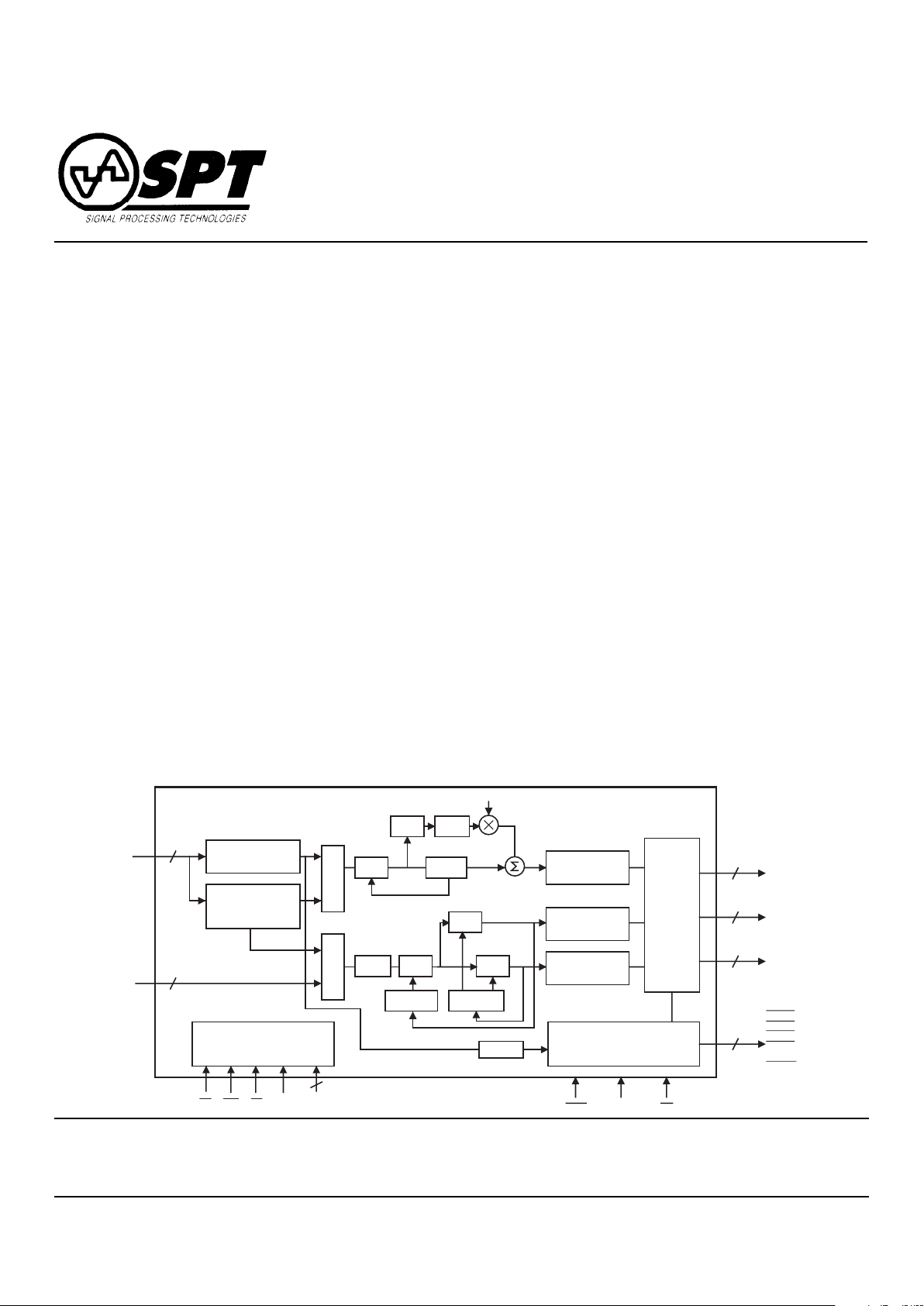
BLOCK DIAGRAM
APPLICATIONS
• High-End NTSC or PAL Video Decoding
• S-Video Decoding
• Composite Video Decoding
• Video Frame Grabbers
• Video Projection and Displays
• Digital VCRs
• Digital Video Transmitters
• Video Printers
• Image Filing Systems
• Multimedia PCs
• Advanced Set-Top Boxes
• Security Cameras
GENERAL DESCRIPTION
The SPT2110 is a high-performance video digital signal
processor for NTSC and PAL applications. It processes 9-bit
composite digitized video or two 9-bit component digitized
video signals. All internal processing is done at 9 or more bits.
The decoder outputs the image data in YCrCb (4:2:2) or RGB
(4:4:4) formats. This product has many advanced internal
features not found in other decoder products. These features
include full 9-bit processing, AGC on both luminance and
chrominance processing, exceptional picture quality controls, complete timing generation and a simple MPU interface. All these features provide for easy digital video design
and produce digital image data that is free from dot error and
color noise. The SPT2110 video decoder is ideal for composite or S-Video applications requiring high quality signal decoding.
M
u
x
Trap Filter
M
u
x
Y/C Separator
(Comb)
Sample Alignment
Sample Alignment
Timing Generation
Control Parameter Registers
Color
Space
Conversion
MPU Interface
HSYNC
VSYNC
HBLNK
VBLNK
ODD
STATUS
9
9
CHR8 - 0
8
R Y
G Cr/Cb
B
5
8
8
8
Sample Alignment
CS WR RD RS D7-0
ClockReset OE
CBPF ACC
Demod
Demod
DTO
Burst
Comp
Sync Det
AGC
BPF
Coring
Peaking
LUM8 - 0
SYNC
SEP
Page 2
SPT
2 3/27/98
SPT2110
The SPT2110 is part of a three-chip solution for high quality
video signal decoding. The companion integrated circuits are
the SPT9210, a dual analog video processor, and the
SPT7852, dual 10-bit ADC. The SPT9210 provides internal
DC restoration and Automatic Gain Control (AGC) of the
video signal. The SPT7852 provides 10-bit resolution video
digitization.
The SPT2110 operates from a single +3.3 V supply. It is
available in a 100-lead PQFP package and operates over the
commercial temperature range.
GENERAL OVERVIEW
The SPT2110 video decoder is compatible with NTSC or PAL
video standards. It has two 9-bit digitized video inputs busses
and three 8-bit video data output busses with sync, blank,
field indicator and chrominance data indicator output signals.
The SPT2110 is fully programmable through the command
registers. Each command register is accessed by a single
address register. The control lines and the bidirectional 8-bit
data bus provide access to the command and address
registers.
DIGITAL VIDEO INPUT DATA BUSSES
The two 9-bit digital video input data busses have 3.3 volt
compatible logic levels. In composite mode, the composite
digital video is input through the LUM8…0, 9-bit data bus. In
component mode, the luminance component is input through
the LUM8…0, 9-bit data bus while the chrominance component is input through the CHR8…0, 9-bit data bus. Register 1
selects whether composite or component video input data will
be processed. The input busses expect valid data on each
rising edge of the clock input. Refer to the timing diagram,
figure 1.
Table I - Digital Image Input Busses Description
Bus Label Description
LUM8...0 Digitized video data for composite
video or the luminance signal input.
LUM8 is the MSB, and LUM0 is the LSB.
CHR8...0 Digitized video data for the chromi-
nance signal input. CHR8 is the MSB,
and CHR0 is the LSB.
DECODED DIGITAL VIDEO OUTPUT DATA
BUSSES
The three 8-bit digital video output data busses on the
SPT2110 have 3.3 volt compatible logic levels. All three
busses are used for RGB digital video data output. Two
busses are used for YC (YCrCb) digital video data. The RGB
data is NTSC or PAL video that has been translated to RGB
(4:4:4) format. The YC data is NTSC or PAL video that has
been translated to YCrCb (4:2:2) format. The luminance
portion of the YCrCb output (Y) is output on the Y/R7…0 bus,
and the color difference signal data (Cr and Cb) is output on
the C/B7…0 bus. Cr and Cb are alternately output every other
clock cycle. All three busses may be programmed to a tristate level. Refer to the timing diagram, figure 1.
Table II - Digital Video Output Busses Description
Bus Label Description
Y/R7...0 Decoded video data for Y (luminance) or R
(red). Y/R7 is the MSB, and Y/R0 is the
LSB.
C/G7...0 Decoded video data for C (chrominance)
or G (green). C/G7 is the MSB, and C/G0
is the LSB.
B7...0 Decoded video data for B (blue). B7 is
the MSB, and B0 is the LSB.
VIDEO TIMING OUTPUT SIGNALS
The video timing output signals have 3.3 volt compatible logic
levels. They produce the temporal information that identifies
the spacial position of the video signal. They are used
downstream to synchronize signals and for odd/even field
identification. These discrete output timing control signals
may be programmed as positive or negative true logic or they
may be tri-stated.
The video timing output signals are described in table III. The
signal names are horizontal sync, vertical sync, horizontal
blank, vertical blank, odd/even field indicator and chrominance flag. Refer to timing diagrams 1, 3 and 4.
Page 3

SPT
3 3/27/98
SPT2110
Table III - Timing Control Signal Description
Signal
Label Description
HSYNC This is the horizontal synchronizing signal; its
width is equal to the width of the incoming
digitized video signal.
VSYNC This is the vertical synchronizing signal. 3H time
for NTSC starting after the three H lines of
equalizing pulses and 2.5H time for PAL starting
at beginning of line 1 and line 312.5.
HBLNK This is the horizontal blanking signal. Registers
DH and EH control the start and stop locations
of the active pixels. When this signal is
deasserted the following number of active video
pixels is displayed for the various sampling
modes.
- ITU-R BT.601 720 active pixels
- NTSC square pixel 640 active pixels
- NTSC4Fsc 768 active pixels
- PAL square pixel 768 active pixels
VBLNK This is the vertical blanking signal. Registers FH
and 10H control the start and stop locations of
the active lines.
ODD When active, this signal indicates that the odd
field is being output from the decoder.
CFLAG This signal indicates whether Cb or Cr data is
active.
Note: Due to asynchronous sampling of the video signal, a
periodic deviation of the sync width by one pixel clock may
be generated in HSYNC, VSYNC, HBLNK, VBLNK and
ODD signals.
CLOCK SIGNAL
The clock (CLK) input has is 3.3 volt compatible logic. The
clock is the master time-base controller for the SPT2110. The
SPT2110 synchronizes data input, data output, control signal
out, address and command register modifications and data
processing to the clock. A stable, jitter-free clock signal
should be used.
Table IV - Sample Mode Clock Frequencies
Sampling Mode Input Frequency (MHz)
NTSC Square Pixel 12.2727
NTSC ITU-R (CCIR-601) 13.500
NTSC 4 Fsc 14.3182
PAL Square Pixel 14.7500
PAL ITU-R (CCIR-601) 13.5000
MPU INTERFACE
The SPT2110 provides for microprocessor unit (MPU) based
programming and control through a 3.3 V compatible logic
interface. The MPU interface is comprised of a bidirectional
8-bit data bus and four discrete control registers. A description of this interface is shown in table V.
COMMAND AND ADDRESS REGISTERS
The SPT2110 operational performance is controlled by internal command registers that are accessed through the MPU
interface described above. There is one address register and
20 command registers (0H - 13H). All registers have read/
write capability.
The address register is used to identify the command register
to be operated. This register must be written to first with the
address of the target command register before a read/write
operation can be performed on the command register. Tables
VI and VII describe the normal operation for reading and
writing to the address register.
Most of the command registers control multiple functions, i.e.,
each bit or group of bits within a register controls a chip
function. When modifying a register a read of the register
should be performed first. Then alter the bit(s) while maintaining the rest of the bits in their present state. Finally, write the
modified data back into the register.
Tables VIII and IX describe the operation for reading and
writing to a selected command register. All registers have a
default setting when the STP2110 is reset. For a detailed
description of the functions of each register, refer to table XIII,
Command Register Description Table.
Page 4

SPT
4 3/27/98
SPT2110
Table V - MPU Interface Description
Signal Name Abbreviation Description
CHIP SELECT CS_ The Chip Select signal (active low logic) enables further action by the chip from the other
control lines This means the chip needs to process (recognize) one of the following
control signals: RS, WR_ or RD_.
REGISTER RS The Register Select signal (active high logic) enables access to the Command Register
SELECT that the address register is holding. When this signal is low it enables the address data
register.
WRITE WR_ The Write signal (active low logic) transfers the data on the data bus into the address or
command data register (depending on the level of RS).
READ RD_ The Read signal (active low logic) transfers the data in the address or command data
register (depending on the level of RS) onto the data bus.
DATA(7-0) D7-0 This is the 8-bit bidirectional data bus for transferring data to and from the SPT2110. The
direction is dictated by the WR_ (input) and RD_ (output) signals.
Refer to the Electrical Specification Table for correct interfacing of the SPT2110. Note the assert times required for each of
the control lines. The times must be a numerical multiple of the clock that operates the SPT2110.
The accessing of a Command register(s) is performed as shown in table VI below.
(Note that 1 defines logic high, 0 is logic low, X is defined as don’t care and D is valid data)
Table VI - Write Address Register
CONT.
STATE\
STEP CS_ WR_ RD_ RS DATA (7-0) COMMENTS
1 0110DDh
2 0010DDh Data needs to be valid on the data bus for minimum setup time
(relative to the WR_ signal).
3 0110DDh Data needs to remain valid on the data bus for minimum hold
time (relative to the WR_ signal).
4 111XXXh Completed Address Write
The address write sequence described above is a normal write sequence. A write can be performed by asserting
CS_ and RS (to logic low). Observe the minimum setup time before asserting WR_. Hold CS_ and RS for the hold
time and then release CS_ and RS. Then set the data bus to the valid address for the minimum setup time before
the rising edge of WR_. Then hold the data bus for the hold time required. Note that the WR_ assert time is a
multiple of the clock. This sequence will perform a valid write to the address register. The following read write
functions may be performed in a manner similar to the normal sequences outlined in the tables VII and VIII.
Table VII - Read Address Register
CONT.
STATE\
STEP CS_ WR_ RD_ RS DATA (7-0) COMMENTS
1 0110XXh
2 0100DDh Data is valid on the data bus after output delay time (relative to
the RD_ signal).
3 0110XXh Data continues to remain valid for output hold time delay (relative
to the RD_ signal).
4 111XXXh Completed Address Read.
Page 5

SPT
5 3/27/98
SPT2110
The following assumes the address register is already set.
Table VIII - Write Command Register
CONT.
STATE\
STEP CS_ WR_ RD_ RS Data (7-0) Comments
1 0111DDh
2 0011DDh Data needs to be valid on the data bus for minimum setup time
(relative to the WR_ signal).
3 0111DDh Data needs to remain valid on the data bus for minimum hold
time (relative to the WR_ signal).
4 111XXXh Completed Command Write.
Table IX - Read Command Register
CONT.
STATE\
STEP CS_ WR_ RD_ RS Data (7-0) Comments
1 0111XXh
2 0101DDh Data is valid on the data bus after output delay time (relative to
the RD_ signal).
3 0111XXh Data continues to remain valid for output hold time delay (relative
to the RD_ signal).
4 111XXXh Completed Command Read.
If the address already contains the correct address of the register to be accessed, it is not necessary to perform
an address register write. Only a command register acquisition is required to write or read the command register.
OTHER DISCRETE SIGNALS
The other signals not discussed are the Reset, Status and OE signals. The following table describes these functions.
Table X - Other Discrete Signals
Signal Input/
Name Output Description
RESET_ INPUT This signal is an input active low. It requires three or more input clocks while the signal
is active to reset the device. It resets all registers to their default states and clears all
data within the device.
STATUS_ OUTPUT This signal is an output active low signal. It will be asserted whenever video sync is
being detected and will go inactive when sync is not detected.
OE_ INPUT When asserted, this signal enables the output signals. This is an active low logic signal.
It tri-states the outputs when deasserted and enables them when asserted. The signals
that are controlled are the data output busses (RGB/YC), HSYNC, VSYNC, HBLNK,
VBLNK, ODD and CFLAG.
Page 6

SPT
6 3/27/98
SPT2110
LUMINANCE PROCESSING
LUMINANCE SEPARATION
For composite video the luminance needs to be separated
from chrominance in the baseband video. Each is processed
separately. Selection of the separation method is determined
by register 3H. Separation of the luminance from the chrominance is performed by a 2H comb, 1H comb or trap filter.
Comb filtering is available for NTSC signal processing only.
The comb is the best filter method for composite video. The
trap filter method of separation reduces the dynamic performance of the luminance signal above 2.3 MHz due to the filter
transfer function.
This separation is not necessary for component (Y/C, S-Video).
The comb filtering is inhibited, and the digitized data is sent
on to the luma processing circuitry.
SYNC SEPARATOR
The sync signals are separated from the luminance component and sent to the timing control circuit. The sync pulses are
used to synchronize the timing of the number of pixels per
line, number of lines, and odd field identification.
LUMINANCE MUX
A 2:1 mux is used to multiplex the digital luminance component data to either the trap filter or comb filter.
AGC
Automatic Gain Control (AGC) for the luminance signal is
derived from the amplitude of the sync signal. The video
luminance is scaled by the value derived from the sync signal
value. This is a very important feature for nonstandard video
signal values. In addition, the sync is removed from the
luminance signal at this stage before further luminance
processing.
PICTURE QUALITY FUNCTIONS
LUMINANCE SIGNAL CORRECTION
Luminance signal correction is composed of three luminance
digital signal processing functions. These functions include
selecting a frequency pass band that will be further enhanced, a coring function and a peaking function. The peaking function must be set to a compensation value (other than
zero, default) for either of the other two functions to be
enabled. The Pass-Band (PBAND) Filter is controlled by
register 6H. It sets the lower limit of the pass band filter. These
frequencies will be peaked further downstream. The coring
function provides a hysteresis effect on pixel-to-pixel data
value changes based on a threshold coring level set by the
core register 7H. Coring is performed on the pre-peaked
signal levels. With the pass-band and the coring levels set,
the peaking compensation value is applied to those luminance signals that fit in the selected profile. Peaking is a
multiplicative factor that gains up the selected frequencies.
The higher the peaking factor the more gain provided for
those selected frequencies. Peaking is controlled by register
8H.
Brightness is controlled by register 12H. This puts an additive
value to the luminance signal. This additive value is plus or
minus 32 LSBs of the luminance signal. It is a DC value for the
luminance signal. Brightness is applied after luminance signal correction is performed.
Contrast is controlled by register 11H. This setting applies a
multiplying factor to the luminance signal. The coefficient
multiplies the luminance value after it has been corrected.
SYNC REINSERTION
The sync signals are reinserted into the luminance signal
after all luminance signal processing is performed.
LUMINANCE SAMPLE ALIGNMENT
Sample alignment circuitry ensures the same number of
pixels per line and field/frame. Counting registers control this
process based on the mode of operation. They determine the
number of pixels per line and the number of lines per field.
LUMINANCE COLOR SPACE CONVERSION
The color space conversion block uses the luminance signal’s
value to transform from the NTSC or PAL system format that
was originally digitized to either RGB of YCrCb. This process
requires the values of both luminance and chrominance be
synchronized in time to make this conversion correctly. The
transformation to RGB or YCrCb is performed using the
luminance and color difference signal data.
CHROMINANCE PROCESSING
COLOR SEPARATION
For composite video, the chrominance needs to be separated
from luminance in the baseband video. Each is processed
separately. Selection of the separation method is determined
by register 3H. Separation of the chrominance from the
luminance is performed by a 2H or 1H comb filter or the trap
filter. The comb separation is the best separation method for
composite video. Comb filtering is available for NTSC signal
processing only.
For component (Y/C, S-Video), this separation is not necessary. The comb filter is inhibited and the digitized chrominance data is sent on for chroma processing.
Page 7

SPT
7 3/27/98
SPT2110
COLOR BAND PASS FILTER
Color band-pass filters ensure that only the chrominance
signal frequencies are passed on to the demodulators.
AUTOMATIC COLOR CONTROL
Automatic color control (ACC, or AGC of the chrominance
signals) is enabled by register AH. The process is used to
monitor the amplitude of the burst signal level. The amplitude
of the color burst is expected to be of a specific amplitude.
When this amplitude is not of the correct level, an adjustment
of the color amplitude is made. This, in turn, corrects the
amplitude of the entire color level pre-demodulated color
signal.
COLOR DEMODULATION
Chrominance demodulation is performed by a quadrature
amplitude demodulator. The demodulation is performed by a
multiplication of the incoming signal with the value of the local
Discrete-Time Oscillator (DTO). This local oscillator is multiplied with the 9-bit chrominance data to provide quadrature
demodulation. This multiplication produces a chrominance
signal that has a data bit width of the sum of the two
multiplying terms. This resultant value is rounded and lowpass filtered. The low pass filter produces the color difference
signals (I and Q, for NTSC and U and V for PAL). To
demodulate the two difference color signals, there is a
separate demodulator for each path. Each has a local oscillator signal that is 90 degrees out of phase with the other and
synchronous with the burst signal.
DISCRETE TIME OSCILLATOR
An on-board Discrete-Time Oscillator (DTO) provides two
color subcarrier local oscillators phase shifted 90°. The DTO
is synchronized with the color burst (color reference) signal
with a digital phase-locked loop.
COLOR SATURATION
Color saturation (amplitude) is controlled by register 9H. The
value of the register is a multiplicative of the color difference
signals produced from the demodulators.
COLOR HUE
Color hue (angle of the color position) is performed post
demodulation with a vector multiplication process. This ensures
accurate hue control for the NTSC and PAL system format.
COLOR BURST DETECTION & PHASE
Monitoring of the color burst is a continuous process. The
burst is evaluated for amplitude to ensure that color information is being processed. See the Color Kill section. The burst
signal is phase-locked to the local DTO. Without a color burst
synchronized local oscillator, the demodulation of the chroma
signal will not be correct.
COLOR KILL
The color information is controlled by register BH. It may be
killed (turned-off) by setting a bit in the register or allowed to
automatically be shutdown if the burst level is not the proper
amplitude.
CHROMINANCE SAMPLE ALIGNMENT
Sample alignment circuitry ensures the same number of
chroma pixels per line and lines/field. Counting registers,
based on the mode of operation, determine the number of
pixels per line and the number of lines per field.
CHROMINANCE COLOR SPACE CONVERSION
The color space conversion block uses the chrominance
difference signal values to transform from the NTSC or PAL
system format that was originally digitized to either RGB or
YCrCb. This process requires the values of both luminance
and color difference signals to be synchronized in time to
make this conversion correctly. The transformation to RGB or
YCrCb is performed using the I and Q (for NTSC) or U and V
(for PAL) color difference signals.
SYNCHRONIZATION AND FIELD DETECTION
Both incoming horizontal and vertical synchronization signals are detected to create the timing for the decoder. The
timing is necessary to produce the correct number of pixels
per line and the correct number of lines per field/frame and to
determine which field (odd or even) is being output. This
maps the image into the final digital storage format.
Timebase generation is digitally controlled using a fixed clock
data sampling scheme with digital phase-locked loop to
control the internal digital shifting of the sampled data. The
data from the luminance and chrominance signals are processed by the sample alignment circuit to ensure the same
number of pixels per line and lines/field. The robust timebase
generation circuitry can operate over a wide range of video
source quality levels. This may include VCR fast-forward and
pause modes.
Page 8

SPT
8 3/27/98
SPT2110
Table XII - SPT2110 Command Register Function Summary
Register Address Bit Function
CHIP MASTER CONTROL
RESET 00H 1 Data Path Reset
0 Reset Device
INPUT MODE CONTROL
MODEA 01H 3 Select NTSC/PAL
2, 1 Select Sampling Frequency
0 CVBS / S-Video Mode Select
OUTPUT MODE CONTROL
MODEB 02H 6 Timing Signal Sync / Free Run Mode Select
5 Select Output Data Format of Cr, Cb (Binary/2's Complement)
4 YC / RGB Output Mode Select
3 Select Data Offset of 16
2 Select Range of Output Limit
1 Reserved
0 Order of Cr, Cb Output
FILTER CONTROL
YCSEL 03H 1, 0 Select YC Separation Method
TIMING SIGNAL POLARITY CONTROL
SYNCP 04H 5 Set CBFlag Polarity
4 Set ODD Polarity
3 Set VBLNK Polarity
2 Set VSYNC Polarity
1 Set HBLNK Polarity
0 Set HSYNC Polarity
SPT2110 COMMAND REGISTERS
The SPT2110 is fully programmable through a standard
MPU interface, (i.e., multiplexed 8-bit address and data bus).
Interface to the command register bus is provided through
this interface. (See the Command and Address Registers
section.)
The command register allows for real-time control of the chip
state, input/output formats, video timing, and video processing parameter values. Table XII is a summary of the command register functions for the SPT2110. Table XIII provides
a detail functional description of each register and its reset/
default settings.
OPERATIONAL MODES
The following table outlines the operational modes of the
SPT2110 video decoder. Operational modes are set by
register IH.
Table XI - SPT2110 Operational Modes
MODE DESCRIPTION
SQUARE PIXEL Maintains proper NTSC or PAL as-
pect ratio for PC monitor scaling.
ITU-R BT.601 Provide support for ITU-R BT.601
(CCIR-601) (CCIR-601). NTSC active number of
pixels is 720 x 480 and PAL active
number of pixels is 720 x 512.
4Fsc (NTSC format only.) Sampling at four
times the color subcarrier mode.
Page 9

SPT
9 3/27/98
SPT2110
Table XII - SPT2110 Command Register Function Summary (Continued)
Register Address Bit Function
PICTURE QUALITY CONTROLS
ADDRESS5 05H 0 Automatic Gain Control On/off
PBAND 06H 2 - 0 Select Contour Compensation Frequency Band
CORE 07H 2 - 0 Core Ring Level
PFACT 08H 2 - 0 Peaking Compensation Coefficient
CGAIN 09H 7 - 0 Color Signal Gain Value
ACC 0AH 0 Automatic Color Control On/Off
CKILL 0BH 0 Select Color Kill Mode
HUE 0CH 7 - 0 Hue Adjustment
VIDEO OUTPUT TIMING SIGNAL CONTROL
HBKBG 0DH 7 - 0 Horizontal Blank Start Position Adjustment
HBKWD 0EH 7 - 0 Horizontal Blank Width Adjustment
VBKBG 0FH 7 - 0 Vertical Blank Start Position Adjustment
VBKEN 10H 7 - 0 Vertical Blank End Position Adjustment
LUMINANCE CONTROLS
CONT 11H 7 - 0 Contrast Adjustment
BRI 12H 5 - 0 Brightness Adjustment
OUTPUT BUFFER STATE CONTROL
HZSET 13H 7 Set R/Y and G/C Output to High Impedance
6 Set B Output to High Impedance
5 Set HSYNC Output to High Impedance
4 Set VSYNC Output to High Impedance
3 Set HBLNK Output to High Impedance
2 Set VBLNK Output to High Impedance
1 Set ODD Output to High Impedance
0 Set STATUS and CFLAG Outputs to High Impedance
Page 10

SPT
10 3/27/98
SPT2110
Table XIII - SPT2110 Command Register Description Tables
Address Bit # Function Bit Setting/Description Default
CHIP MASTER CONTROL
00H 1 Resets the data Paths. Command register 0 Normal Operation 00H
values remain unchanged. 1 Data Path Reset
RESET 0 Resets the entire chip including digital data 0 Normal Operation
path and resets the command registers to their
default values
1 Data Path and Command
Register Reset
INPUT MODE CONTROL
01H 3 NTSC/PAL 0 NTSC 02 H
Selects between NTSC and PAL modes 1 P AL
MODE A 2,1 Sampling Mode Select 0 0 4Fsc
01 Square Pixel
10 CCIR601
11 Not Used (CCIR601)
0 Composite or Component Video Input Select 0 CVBS
1 S-Video
Address Bit # Function Bit Setting/Description Default
OUTPUT MODE CONTROL
02H 6 Free Run. Enables free run of video output
timing signal:HSYNC, VSYNC, 0 Normal Operation
00H
MODE B HBLNK, VBLNK, ODD 1 Timing Signal Free Run
5 Cr, Cb Signal Format. Sets the data 0 Offset Binary
format for the Cr, Cb digital output data. 1 Two’s Complement
4 YC/RGB Output Mode. Sets the output to 0 YCrCb Output mode
either YC or RGB. 1 RGB output Mode
3 Offset Data. Sets between data output 0 No Data Output Offset
offset by 16 or no offset. 1 Offset Data Output by 16
2 Range of Output Limit. Sets the minimum
and maximum values allowed in the output
data.
0 Brightness Signal (Including
RGB) 16 - 235,
Color Difference Signal
16 - 224
1 Brightness Signal (Including
RGB) 1 - 254,
Color difference signal
1 - 254
1 Reserved Used by fixing at 0
0 Order of Cr, Cb 0 Starting with Cr (Cr shortly
after HSYNC)
1 Starting with Cb
FILTER CONTROL
03H 1,0 YC Separation Method. Selects YC
separation.
00 YC separation by 2H comb
filter
00H
YCSEL 01 YC separation by trap filter
10 YC separation by 1H comb
Filter
11 Not used at this time
Page 11

SPT
11 3/27/98
SPT2110
Table XIII - SPT2110 Command Register Description Tables (Continued)
OUTPUT MODE CONTROL
04H 5 CFLAG Active Flag Polarity (Cb active) 0 Positive 00H
SYNCP 1 Negative
4 ODD Field Active Polarity 0 Positive
1 Negative
3 VBLNK Polarity 0 Negative
Vertical Blank Signal Polarity 1 Positive
2 VSYNC Polarity. 0 Negative
Vertical Sync Signal Polarity 1 Positive
1 HBLNK Polarity 0 Negative
Horizontal Blank Signal Polarity 1 Positive
0 HSYNC Polarity 0 Negative
Horizontal Sync Signal Polarity 1 Positive
05H 0 Automatic Gain Control 0 On 00H
1 Off
Address Bit # Function Bit Setting/Description Default
PICTURE CONTROL
06H 2 -0 Sets Contour Compensation Frequency Band. 00 0 1/2 (Intermediate band) 0 2H
001 1/4
PBAND 01 0 0
01 1 -1/4
1XX -1/2 (High band)
07H 2-0 Core Ring Level 000 0 LSB 00H
Number of LSB values for coring 001 2 LSB
CORE 01 0 3 LSB
01 1 4 LSB
10 0 5 LSB
10 1 6 LSB
08H 2 -0 Peaking Compensation Coefficient 00 0 0 00H
Gain Factor for High Frequency Luminance 001 1/4
PFACT 010 1/2
011 3/4
100 1
101 5/4
110 3/2
111 2
COLOR CONTROL
09H
CGAIN
7-0 Color Signal Gain 0 - 255 Gain setting value with
128 as 100% (saturation)
80H
0AH 0 Automatic Color Control Select 0 ACC on 00H
ACC 1 ACC off
0BH 0 Color Kill Mode Select 0 Auto Color Kill Mode 00H
CKILL 1 Color Off
0CH 7-0 Hue Adjustment ±90° Phase adjustment, 90°/128
degree step (signed two’s
complement)
80H = +90°
7FH = -90°
00H
Page 12

SPT
12 3/27/98
SPT2110
Table XIII - SPT2110 Command Register Description Tables (Continued)
SYNC/BLANK OUTPUT CONTROL
0DH
HBKBG
7-0 Horizontal Blank Start position compensation -128 (80H) to 127 (7FH)
(signed two’s complement)
00H
0EH
HBKWD
7-0 Horizontal Blank width Compensation -128 (80H) to 127 (7FH)
(signed two’s complement)
00H
0FH
VBKBG
7-0 Vertical Blank Start Position Compensation -128 (80H) to 127 (7FH)
(signed two’s complement)
00H
10H
VBKEN
7-0 Vertical Blank END Compensation -128 (80H) to 127 (7FH)
(signed two’s complement)
00H
LUMINANCE CONTROL
11H
CONT
7-0 Contrast Adjustment Coefficient 80H = 1.0000000 as 100%
00H to FFH
80H
12H
BRI
5-0 Brightness Adjustment -32 (20H) to 30 (1FH)
(signed two’s complement)
00H
Address Bit # Function Bit Setting/Description Default
OUTPUT BUFFER STATE CONTROL
13H 7 R/Y and G/C Output to High Z Select 0 Output Enable 00 H
1 Output High Z
HZSET 6 B Output to High Z Select 0 Output Enable
1 Output High Z
5 HSYNC Output to High Z Select 0 Output Enable
1 Output High Z
4 VSYNC Output to High Z Select 0 Output Enable
Notes: 1 Output High Z
All 3 HBLNK Output to High Z Select 0 Output Enable
Outputs 1 Output High Z
are 2 VBLNK Output to High Z Select 0 Output Enable
High Z 1 Output High Z
with OE 1 ODD Output to High Z Select 0 Output Enable
set to 1 Output High Z
logic 0 STATUS and CFLAG Outputs to High Z Select 0 Output Enable
High 1 Output High Z
Page 13

SPT
13 3/27/98
SPT2110
CLK
LUM8...0,
CHR8...0
(INPUT)
Y/R7...0, C/G7...0,
B7...0, HSYNC,
VSYNC, HBLNK,
VBLNK, STATUS,
CFLAG, ODD
(Output)
t
ch
t
cl
t
clk
t
od
t
is
t
ih
Figure 1 - Input and Output Timing Diagram
Page 14

SPT
14 3/27/98
SPT2110
Register Read Cycle
CS_
RS
Data
(8-Bit)
WR_
RD_
Address
Data
Address
Write
t
rss
t
rsh
t
css
t
csh
t
rl
t
rh
t
dbod
t
dboh
t
dboz
Data
Read
CS_
RS
Data
(8-Bit)
WR_
Address Data
Address
Write
Data
Write
t
css
t
csh
t
dbs
t
dbh
t
wl
t
wh
trsh
t
rss
t
css
t
csh
t
dbs
t
dbh
Register Write Cycle
Figure 2 - MPU Interface Signal Timing Diagram
Page 15

SPT
15 3/27/98
SPT2110
Figure 3 - Sync Signal Output Timing (NTSC) Standard Signal Input
HSYNC
VSYNC
ODD
HBLNK
VBLNK
YCbCr
RGB
5235245251234567 1920212223
NTSC Odd Field
HSYNC
VSYNC
ODD
HBLNK
VBLNK
YCbCr
RGB
261 262 263 264 265 266 267 268 269 270 282 283 284 285 286
NTSC Even Field
Figure 4 - Sync Signal Output Timing (PAL), Standard Signal Input
HSYNC
VSYNC
ODD
HBLNK
VBLNK
YCbCr
RGB
6206216226236246251234 2223242526
PAL Odd Field
HSYNC
VSYNC
ODD
HBLNK
VBLNK
YCbCr
RGB
308 309 310 311 312 313 314 315 316 317 335 336 337 338 339
PAL Even Field
Page 16

SPT
16 3/27/98
SPT2110
Figure 5 - Typical Interface Circuit
Y/RC7
Y/RC6
Y/RC5
Y/RC4
Y/RC3
Y/RC2
Y/RC1
Y/RC0
C/G7
C/G6
C/G5
C/G4
C/G3
C/G2
C/G1
C/G0
B7
B6
B5
B4
B3
B2
B1
B0
VSS
VSS
VSS
VSS
VSS
VSS
VSS
VSS
VSS
VSS
VSS
VSS
VSS
VDD
VDD
VDD
VDD
VDD
VDD
VDD
VDD
LUM8
LUM7
LUM6
LUM5
LUM4
LUM3
LUM2
LUM1
LUM0
CHR8
CHR7
CHR6
CHR5
CHR4
CHR3
CHR2
CHR1
CHR0
CLOCK
D7
D6
D5
D4
D3
D2
D1
D0
CS_
RS
RD_
WR_
OE_
ODD
RESET_
13
16
17
18
19
20
21
22
23
15
35
45
62
74
77
91
99
47
48
49
52
53
54
55
56
37
38
39
40
41
42
43
44
27
28
29
30
31
32
33
34
66
11425263646505160757690100
6769656471
70
HSYNC_
VSYNC_
HBLNK_
VBLNK_
STATUS_
CFLAG
12
11
10
9
88
87
86
85
84
83
82
81
80
6
5
4
3
2
96
95
94
93
61
8
SPT2110
Video
Decoder
BUFFER
AND/OR
LOGIC
LEVEL
TRANSLATOR
8
BUFFER
AND/OR
LOGIC
LEVEL
TRANSLATOR
8
BUFFER
AND/OR
LOGIC
LEVEL
TRANSLATOR
8
SPT7852.38
SPT7852.37
SPT7852.36
SPT7852.35
SPT7852.34
SPT7852.33
SPT7852.32
SPT7852.31
SPT7852.30
SPT7852.18
SPT7852.19
SPT7852.20
SPT7852.21
SPT7852.22
SPT7852.23
SPT7852.24
SPT7852.25
SPT7852.26
SPT7852.28
FROM:
POWER-ON
RESET,
SYSTEM
RESET
AND/OR
MPU CONTROL
RESET
TO: SYSTEM PROCESSOR TO
VERIFY VIDEO IS BEING DETECTED
3.3 V
******
(LUMINANCE
OR COMPOSITE
DIGITIZED VIDEO
FROM "A"
SECTION OF
SPT7852)
(CHROMINANCE
DIGITIZED VIDEO
FROM "B"
SECTION OF
SPT7852)
(LUMINANCE
OR RED
DECODED
VIDEO)
(CHROMINANCE
OR GREEN
DECODED
VIDEO)
(RED
DECODED
VIDEO)
8
FROM MPU DATA BUS
FROM MPU CONTROL
FROM MPU CONTROL
FROM MPU CONTROL
FROM MPU CONTROL
FROM MPU CONTROL
TO: VIDEO DATA CONTROL AND
TIMING CIRCUIT
(DECODED VIDEO
DATA CAN GO TO
FIFO, RAM, VIDEO
ENCODER, ETC.)
DIGITAL GROUND, CONNECTED DIRECTLY TO DIGITAL GROUND PLANE
NOTES:
* DECOUPLING AND FILTER CAPACITORS LOCATED AS CLOSE TO THE DECODER AS POSSIBLE WITH SHORT PATH TO GROUND
VALUE OF 0.1 µF.
BUFFER
AND/OR
LOGIC
LEVEL
TRANSLATOR
5
TO: VIDEO ENCODING
CIRCUITRY
Page 17

SPT
17 3/27/98
SPT2110
SPT2110 NTSC/PAL VIDEO DECODER PIN FUNCTIONS
Signal Name Pin Numbers I/O Function
Data I/O
LUM8...0 80-88 I Composite Video or Luminance Signal Input (LUM0 = LSB)
CHR8...0 2-6, 93-96 I Chrominance Signal Input (CHR0 = LSB)
Y/R7...0 47-49 O Luminance (Y) Data or R Data Output (RGB Mode)
52-56 (High Z when OE_ = 1) (Y/R0 = LSB)
C/G7...0 37-44 O Color (Cr/Cb) Data or G Data Output (RGB Mode)
(High Z when OE_ = 1) (C/G0 = LSB)
B7...0 27-34 O B Data Output (RGB Mode) (High Z when OE_ = 1) (B0 = LSB)
Clock and Sync Signals
CLOCK 61 I Clock Input
HSYNC_ 70 O Horizontal Sync Signal (High Z when OE_ = 1)
VSYNC_ 71 O Vertical Sync Signal (High Z when OE_ = 1)
HBLNK_ 64 O Horizontal Blanking Signal (High Z when OE_ = 1)
VBLNK_ 65 O Vertical Blanking Signal (High Z when OE_ = 1)
ODD 66 O Field Identification Signal (EVEN/ODD) (High Z when OE_ = 1)
CFLAG 69 O Logic 1 when Cb output is generated (positive polarity)
STATUS_ 67 O Flag indicating sync detection when low.
MPU Interface
OE_ 13 I Output Enable: 0-Normal Output Mode
1-Specified output pins set to high impedance state
CS_ 12 I Chip Select (Active Low)
RS 11 I Register Select: 0-Address register access
1-Address register specified data register accessed
RD_ 10 I Read Control (Active Low)
WR_ 9 O Write Control (Active Low)
D7...0 16-23 I/O Data Bus/Register Address
RESET_ 8 I Reset Terminal (Active Low)
Power Supply Connections
V
DD
15, 35, 45, 62, 74, - +3.3 V Power Supply
77, 91, 99
V
SS
1, 14, 25, 26, 36, - Digital Ground
46, 50, 51, 60,
75, 76, 90, 100
N/C 7, 24, 57-59,63, - No Connect
68, 72, 73,78, 79,
89, 92, 97, 98
Page 18

SPT
18 3/27/98
SPT2110
1
51
76
26
GND
CHR4
CHR5
CHR6
CHR7
CHR8
N/C
Reset_
WR_
RD_
RS
CS_
OE_
GND
V
DD
D7
D6
D5
D4
D3
D2
D1
D0
N/C
GND
GND
V
DD
N/C
N/C
VSYNC_
HSYNC_
CFLAG
N/C
STATUS_
ODD
VBLNK_
HBLNK_
N/C
V
DD
CLK
GND
N/C
N/C
N/C
Y/R0
Y/R1
Y/R2
Y/R3
Y/R4
GND
GND
B7
B6
B5
B4
B3
B2
B1
B0
V
DD
GND
C/G7
C/G6
C/G5
C/G4
C/G3
C/G2
C/G1
C/G0
V
DD
GND
Y/R7
Y/R6
Y/R5
GND
CHR2
CHR1
CHR0
N/C
V
DD
GND
N/C
LUM8
LUM7
LUM6
LUM5
LUM4
LUM3
LUM2
LUM1
LUM0
N/C
N/C
V
DD
GND
V
DD
N/C
N/C
GND
CHR3
100
75
50
25
SPT2110 PIN OUT
100L PQFP
Page 19

SPT
19 3/27/98
SPT2110
ELECTRICAL SPECIFICATIONS
TA=25°C, VDD = +3.3 V, unless otherwise specified.
TEST TEST
PARAMETERS CONDITIONS LEVEL MIN TYP MAX UNITS
Digital Inputs
Reset Pin
V
IH
VDD - 0.7 V
V
IL
0.7 V
I
IH
VIH = V
DD
-10 µA
I
IL
VIL = V
SS
10 µA
Clock Pin
V
IH
2.0 V
V
IL
0.8 V
I
IH
VIH = V
DD
-10 µA
I
IL
VIL = V
SS
10 µA
All Other Inputs
V
IH
VDD - 1.0 V
V
IL
1.0 V
I
IH
VIH = V
DD
-10 µA
I
IL
VIL = V
SS
10 µA
Digital Outputs
V
IH
IOH = -4 mA VDD - 0.5 V
V
IL
IOL = +4 mA 0.5 V
Power Supply
V
DD
3.0 3.6 V
I
DD
VDD=+3.3 V 70 100 mA
Timing Characteristics
CS Setup (TCSS) 10 ns
CS Hold (TCSH) 10 ns
RS Setup (TRSS) 10 ns
RS Hold (TRSH) 10 ns
RD/WR Pulse Low (TRWL) 2 X TCC
RD/WR Pulse High (TRWH) 2 X TCC
Delay to Data Bus Valid (TDBV) 25 ns
Data Output Disable (TDOD) 20 ns
Data Output Hold (TDOH) 3 ns
Write Data Setup (TWDS) 10 ns
Write Data Hold (TWDH) 10 ns
Clock Cycle (TCC) 67 ns
Clock Pulse High (TCH) 27 ns
Clock Pulse Low (TCL) 27 ns
Input Data/Cont Setup (TIS) 10 ns
Input Data/Cont Hold (TIH) 4 ns
Output Delay Time (TDRY) Load Capac.=50 pF 7 27 ns
Reset Pulse Width (TRSW) 5 X TCC
ABSOLUTE MAXIMUM RATINGS (Beyond which damage may occur)1 25 °C
Supply Voltages
VDD............................................................ -0.5 to +5.0 V
Input/Output Voltages
Digital Inputs ................................... -0.5 V to VDD +0.5 V
Digital Outputs ................................ -0.5 V to VDD +0.5 V
Note: 1. Operation at any Absolute Maximum Rating is not implied. See Electrical Specifications for proper nominal
applied conditions in typical applications.
Temperature
Operating Temperature.................................... 0 to 70 °C
Junction Temperature ........................................... 175 °C
Lead Temperature, (soldering 10 seconds) .......... 300 °C
Storage Temperature................................-65 to +150 °C
Page 20

SPT
20 3/27/98
SPT2110
ORDERING INFORMATION
PART NUMBER DESCRIPTION TEMPERATURE RANGE PACKAGE TYPE
SPT2110SCT NTSC/PAL Video Decoder 0 to +70 °C 100L PQFP
*Please see the die specification for guaranteed electrical performance.
125
26
50
5175
76
100
A
B
CD
EF
G
H
I
J
L
K
INCHES
MILLIMETERS
SYMBOL MIN MAX MIN MAX
A 0.618 0.642 15.7 16.3
B 0.551 typ 14.0 typ
C 0.618 0.642 15.7 16.3
D 0.551 typ 14.0 typ
E 0.017 0.023 0.42 0.58
F 0.003 0.011 0.08 0.28
G 0.067 max 0.000 1.70 max
H 0.000 0.008 0.00 0.20
I 0.005 0.009 0.12 0.22
J 0.039 typ 0.000 1.00 typ
K 0°6°0°6°
L 0.016 0.024 0.40 0.60
PACKAGE OUTLINE
100-LEAD PQFP
Signal Processing Technologies, Inc. reserves the right to change products and specifications without notice. Permission is hereby expressly
granted to copy this literature for informational purposes only. Copying this material for any other use is strictly prohibited.
WARNING - LIFE SUPPORT APPLICATIONS POLICY - SPT products should not be used within Life Support Systems without the specific
written consent of SPT. A Life Support System is a product or system intended to support or sustain life which, if it fails, can be reasonably
expected to result in significant personal injury or death.
Signal Processing Technologies believes that ultrasonic cleaning of its products may damage the wire bonding, leading to device
failure. It is therefore not recommended, and exposure of a device to such a process will void the product warranty.
 Loading...