

Page 1
Features
■
-3dB bandwidth of 170MHz
■
0.1% settling in 22ns
■
Complete overdrive protection
■
Low power: 570mW (190mW at ±5V)
■
3MΩ input resistance
■
Output may be current limited
■
Direct replacement for CLC205
Applications
■
Fast, precision A/D conversion
■
Automatic test equipment
■
Input/output amplifiers
■
Photodiode, CCD preamps
■
IF processors
■
High-speed modems, radios
■
Line drivers
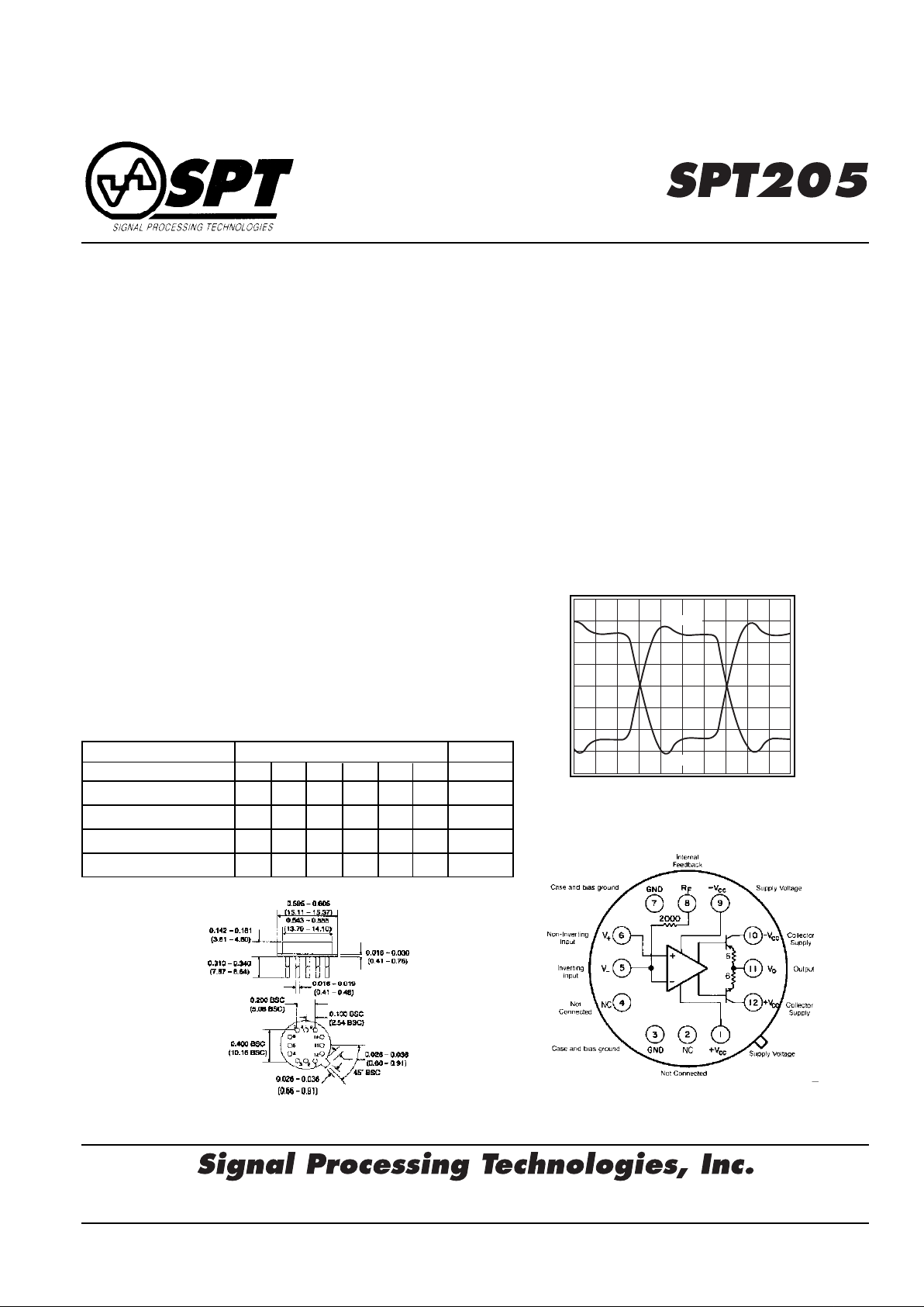
Bottom View
OVERDRIVE-PROTECTED WIDEBAND OP AMP
Package Dimensions
General Description
The SPT205 is a wideband overdrive-protected operational
amplifier designed for applications needing both speed and low
power operation. Utilizing a well-established current feedback
architecture, the SPT205 exhibits performance far beyond that
of conventional voltage feedback op amps. For example, the
SPT205 has a bandwidth of 170MHz at a gain of +20 and
settles to 0.1% in 22ns. Plus, the SPT205 has a combination of
important features not found in other high-speed op amps.
For example, the SPT205 has been designed to consume little
power – 570mW at ±15V supplies. The result is lower power
supply requirements and less system-level heat dissipation. In
addition, the device can be operated on supply voltages as low
as ±5V for even lower power dissipation.
Complete overdrive protection has been designed into the part.
This is critical for applications, such as ATE and instrumentation,
which require protection from signal levels high enough to cause
saturation of the amplifier. This feature allows the output of the
op amp to be protected against short circuits using techniques
developed for low-speed op amps. With this capability, even the
fastest signal sources can feature effective short circuit protection.
The SPT205 is constructed using thin film resistor/bipolar
transistor technology, and is available in the following versions:
SPT205AIH -25 to +85 °C 12-pin TO-8 can
SPT205AMH -55 to +125 °C 12-pin TO-8 can, features
burn-in and hermetic testing
4755 Forge Road, Colorado Springs, Colorado 80907, USA
Phone: (719) 528-2300 FAX: (719) 528-2370 Website: http://www.spt.com E-Mail: sales@spt.com
Typical Performance
Gain Setting
Parameter +7 +20 +50 -1 -20 -50 Units
Bandwidth (-3 dB) 220 170 80 220 130 80 MHz
Rise time 1.7 2.2 4.7 1.7 2.9 4.7 ns
Slew Rate 2.4 2.4 2.4 2.4 2.4 2.4 V/ns
Settling Time (to 0.1%) 22 22 20 21 20 19 ns
Large Signal Pulse Response
Output Voltage (2V/div)
Time (5ns/div)
205 Plot8
Av = +20
Av = -20
Page 2

2 10/9/98
SPT205
PARAMETERS CONDITIONS TYP MIN & MAX RATINGS UNITS SYM
Ambient Temperature SPT205AIH +25°C -25°C +25°C +85°C
Ambient Temperature SPT205AMH +25°C -25°C +25°C +85°C
FREQUENCY DOMAIN RESPONSE
✝ -3dB bandwidth V
o
= <2V
pp
170 >140 >140 >125 MHz SSBW
large-signal bandwidth V
o
= <10V
pp
100 >72 >80 >80 MHz FPBW
gain flatness V
o
= <2V
pp
✝ peaking 0.1 to 35MHz 0 <0.3 <0.3 <0.5 dB GFPL
✝ peaking >35MHz 0 <0.5 <0.5 <0.8 dB GFPH
✝ rolloff at 70MHz – <0.8 <0.8 <0.8 dB GFR
group delay to 70MHz 3.0 ± .2 – – – ns GD
linear phase deviation to 70MHz 0.8 <3.0 <2.0 <3.0 ° LPD
TIME DOMAIN RESPONSE
rise and fall time 2V step 2.2 <2.6 <2.6 <3.0 ns TRS
10V step 4.8 <5.5 <5.5 <5.5 ns TRL
settling time to 0.1% 10V step, note 2 22 <27 <27 <27 ns TS
to 0.05% 10V step, note 2 24 <30 <30 <30 ns TSP
overshoot 5V step 7 <14 <14 <14 % OS
slew rate 20Vpp at 50MHz 2.4 >1.8 >2.0 >2.0 V/ns SR
NOISE AND DISTORTION RESPONSE
✝ 2nd harmonic distortion 2V
pp
, 20MHz -57 <-50 <-50 <-50 dBc HD2
✝ 3rd harmonic distortion 2V
pp
, 20MHz -68 <-55 <-55 <-55 dBc HD3
equivalent input noise
voltage >100kHz 2.1 <3.0 <3.0 <3.5 nV/√Hz VN
inverting current >100kHz 22 <30 <30 <35 pA/√Hz ICN
non-inverting current >100kHz 4.8 <6.5 <6.5 <7.5 pA/√Hz NCN
noise floor >100kHz -157 <-154 <-154 <-153 dBm(1Hz) SNF
integrated noise 1kHz to 150MHz 39 <55 <55 <61 µV INV
noise floor >5MHz -157 <-154 <-154 <-153 dBm(1Hz) SNF
integrated noise 5MHz to 150MHz 39 <55 <55 <61 µV INV
STATIC, DC PERFORMANCE
* input offset voltage 3.5 <8.0 <8.0 <11.0 mV VIO
average temperature coefficient 11 <25 <25 <25 µV/°C DVIO
* input bias current non-inverting 3.0 <25 <15 <15 µΑ IBN
average temperature coefficient 15 <100 <100 <100 nA/°C DIBN
* input bias current inverting 2.0 <22 <10 <25 µA IBI
average temperature coefficient 20 <150 <150 <150 nA/°C DIBI
* power supply rejection ratio 69 >55 >55 >55 dB PSRR
common mode rejection ratio 60 >50 >50 >50 dB CMRR
* supply current no load 19 <20 <20 <22 mA ICC
MISCELLANEOUS PERFORMANCE
non-inverting input resistance DC 3.0 >1.0 >1.0 >1.0 MΩ RIN
non-inverting input capacitance 70MHz 5.0 <7.0 <7.0 <7.0 pF CIN
output impedance DC – <0.1 <0.1 <0.1 Ω RO
output voltage range no load ±12 >±11 >±11 >±11 V VO
internal feedback resistor
absolute tolerance – – <0.2 – % RFA
temperature coefficient – – -100 ±40 – ppm/°C RFTC
inverting input current self limit 2.2 <3.0 <3.0 <3.2 mA ICL
Min/max ratings are based on product characterization and simulation. Individual parameters are tested as noted. Outgoing quality levels are
determined from tested parameters.
Absolute Maximum Ratings Recommended Operating Conditions
V
CC
±20V V
CC
±5V to ±15V
I
o
±75mA I
o
±50mA
common mode input voltage ±(|V
CC
| -1)V common mode input voltage ±(|VCC| -5)V
differential input voltage ±3V gain range +7 to +50, -1 to -50
thermal resistance (see thermal model)
operating temperature AI: -25°C to +85°C note 1: * AI, AM 100% tested at +25°C
AM: -55°C to +125°C ✝ AM 100% tested at +25°C and sample tested
storage temperature -65°C to +150°C at -55°C and +125°C
lead temperature (soldering 10s) +300°C ✝ AI sample tested at +25°C
note 2: Settling time specifications require the use of an
external feedback resistor (2Ω)
SPT205 Electrical Characteristics
(Av = +20V, VCC = ±15V, RL = 200Ω, Rf = 2kΩ; unless specified)
Page 3

3 10/9/98
SPT205
Inverting Frequency Response
Normalized Magnitude (1dB/div)
Phase (45°/div)
Frequency (MHz)
0 20 40 60 80 100 120 140 160 180
200
Gain
Phase
Av = -1
Av = -7
Av = -1
Av = -7
Av = -20
Av = -50
Av = -20
Av = -50
Frequency Response vs. External R
f
Relative Gain (5dB/div)
Frequency (MHz)
0 20 40 60 80 100 120 140 160 180
200
Rf = 1.5kΩ
Av = +7
Av = +50
Av = +20
Rf = 2kΩ
Rf = 3kΩ
Rf = 1.5kΩ
Rf = 2kΩ
Rf = 3kΩ
Rf = 1.5kΩ
Rf = 2kΩ
Rf = 3kΩ
Relative Bandwidth vs. V
CC
Relative Bandwidth
±V
CC
(V)
4 6 8 10 12 14
16
0.2
0.3
0.4
0.5
0.6
0.7
0.8
0.9
1.0
Gain and Phase for Various Loads
Magnitude (1dB/div)
Phase (45°/div)
Frequency (MHz)
0 20 40 60 80 100 120 140 160 180 200
RL = 50Ω
RL = 100Ω
RL = 200Ω
RL = 1kΩ
RL = 1kΩ
RL = 200Ω
RL = 100Ω
RL = 50Ω
Gain
Phase
Small Signal Pulse Response
Output Voltage (0.4V/div)
Time (5ns/div)
Av = +20
Av = -20
Large Signal Pulse Response
Output Voltage (2V/div)
Time (5ns/div)
Av = +20
Av = -20
Settling Time
Settling Error (%)
Time (5ns/div)
10V step
R
f
= 2kΩ (external)
-0.20
-0.15
-0.10
-0.05
0
0.05
0.10
0.15
0.20
2nd and 3rd Harmonic Distortion
Distortion (dBc)
Frequency (MHz)
Vo = 2V
pp
-80
-75
-70
-65
-60
-55
-50
-45
-40
-35
-30
1 10 100
2nd
3rd
2-Tone 3rd Order Intermodulation Intercept
Intercept (dBm)
Frequency (MHz)
20
25
30
35
40
45
0 20 10040 60 80
Equivalent Input Noise
Noise Voltage (nV/√Hz)
Noise Current (pA/√Hz)
Frequency (Hz)
0
10
100
0
10
100
100 1k 100M10k 100k 1M 100
Inverting Current 18.3 pA/√Hz
Non-Inverting Current 2.5 pA/√Hz
Voltage 1.8 nV/√Hz
SPT205 Typical Performance Characteristics
(TA = +25°C, Av = +20, VCC = ±15V, RL = 200Ω; unless specified)
+
T
ambient
θ
ca
T
case
17.5°C/W
T
j(circuit)
P
circuit
200°C/W
T
j(npn)
P
npn
200°C/W
P
pnp
T
j(pnp)
Non-Inverting Frequency Response
Normalized Magnitude (1dB/div)
Phase (45°/div)
Frequency (MHz)
0 20 40 60 80 100 120 140 160 180
200
Gain
Phase
Av = +7
Av = +20
Av = +50
Av = +7
Av = +20
Av = +50
Large Signal Gain and Phase
Magnitude (1dB/div)
Phase (45°/div)
Frequency (MHz)
0 153045607590105120135
150
Vo = 10V
pp
Gain
Phase
CMRR and PSRR
PSRR and CMRR (dB)
Frequency (Hz)
0
20
40
60
80
100
100 1k 100M10k 100k 1M 10M
PSRR
CMRR
Page 4

4 10/9/98
SPT205
Current Feedback Amplifiers
Some of the key features of current feedback technology
are:
■
Independence of AC bandwidth and voltage gain
■
Adjustable frequency response with feedback resistor
■
High slew rate
■
Fast settling
Current feedback operation can be described using a simple
equation. The voltage gain for a non-inverting or inverting
current feedback amplifier is approximated by Equation 1.
Equation 1
where:
■
Av is the closed loop DC voltage gain
■
Rf is the feedback resistor
■
Z(jω) is the SPT205’s open loop transimpedance
gain
■
is the loop gain
The denominator of Equation 1 is approximately equal to
1 at low frequencies. Near the -3dB corner frequency, the
interaction between Rf and Z(jω) dominates the circuit
performance. The value of the feedback resistor has a
large affect on the circuits performance. Increasing Rf has
the following affects:
■
Decreases loop gain
■
Decreases bandwidth
■
Reduces gain peaking
■
Lowers pulse response overshoot
■
Affects frequency response phase linearity
Overdrive Protection
Unlike most other high-speed op amps, the SPT205 is not
damaged by saturation caused by overdriving input
signals (where Vin x gain > max. Vo). The SPT205 self
limits the current at the inverting input when the output is
saturated (see the inverting input current self limit
specification); this ensures that the amplifier will not be
damaged due to excessive internal currents during overdrive.
For protection against input signals which would exceed
either the maximum differential or common mode input
voltage, the diode clamp circuits below may be used.
differential protection
SPT205
+
-
common mode
protection
R
g
+V
cc
V
in
V
o
-V
cc
Figure 1: Diode Clamp Circuits for Common Mode
and Differential Mode Protection
Short Circuit Protection
Damage caused by short circuits at the output may be
prevented by limiting the output current to safe levels. The
most simple current limit circuit calls for placing resistors
between the output stage collector supplies and the
output stage collectors (pins 12 and 10). The value of this
resistor is determined by:
where II is the desired limit current and RI is the minimum
expected load resistance (0Ω for a short to ground).
Bypass capacitors of 0.01µF on should be used on the
collectors as in Figures 2 and 3.
33Ω
+15V
.1
3.9
.01
Capactance in µF
1
12
8
3,7
200Ω
10
11
33Ω
.01
.1
3.9
-15V
9
+
-
SPT205
V
o
Rf = 2000Ω (internal)
6
V
in
5
R
i
50Ω
R
g
A1
R
R
v
f
g
=+
Figure 2: Recommended Non-Inver ting Gain Circuit
33Ω
+15V
.1
3.9
.01
Capactance in µF
1
12
8
5
V
in
3,7
200Ω
10
R
i
11
33Ω
.01
.1
3.9
-15V
9
+
-
SPT205
V
o
Rf = 2000Ω (internal)
6
50Ω
R
g
For Zin = 50Ω, select Rg||Ri = 50Ω
A
-R
R
v
f
g
=
Figure 3: Recommended Inver ting Gain Circuit
A more sophisticated current limit circuit which provides a
limit current independent of RI is shown in Figure 4 on
page 5.
With the component values indicated, current limiting
occurs at 50mA. For other values of current limit (II), select
RC to equal Vbe/lI. Where Vbe is the base to emitter
voltage drop of Q3 (or Q4) at a current of [2VCC – 1.4] / Rx,
where Rx ≤ [(2VCC – 1.4) / II]
B
min
. Also, B
min
is the minimum beta of Q1 (or Q2) at a
current of II. Since the limit current depends on Vbe, which
is temperature dependent, the limit current is likewise
temperature dependent.
V
V
A
1
R
Zj
o
in
v
f
=
+
()
ω
Zj
R
f
ω
()
R
V
I
R
C
C
I
I
=−
Page 5

5 10/9/98
SPT205
Q3
(2N3906)
R
x
14.3kΩ
Q4
(2N3904)
0.01ΩF
0.01ΩF
+V
cc
R
c
12Ω
Q1
(MJE170)
Q2
(MJE180)
R
c
12Ω
-V
cc
to pin 10
to pin 12
Figure 4: Active Current Limit Circuit (50mA)
Controlling Bandwidth and Passband Response
In most applications, a feedback resistor value of 2kΩ
will provide optimum performance; nonetheless, some
applications may require a resistor of some other value.
The response versus Rf plot on the previous page shows
how decreasing Rf will increase bandwidth (and frequency
response peaking, which may lead to instability). Conversely , large values of feedback resistance tend to roll of f
the response.
The best settling time performance requires the use of an
external feedback resistor (use of the internal resistor
results in a 0.1% to 0.2% settling tail). The settling
performance may be improved slightly by adding a capacitance of 0.4pF in parallel with the feedback
resistor (settling time specifications reflect performance
with an external feedback resistor but with no external
capacitance).
Noise Analysis
Approximate noise figure can be determined for the
SPT205 using the
Equivalent Input Noise
plot on page 3
and the equations shown below.
kT = 4.00 x 10
-21
Joules at 290°K
Vn is spot noise voltage (V/√Hz)
in is non-inverting spot noise current (A/√Hz)
ii is inverting spot noise current (A/√Hz)
R
s
R
n
R
o
R
f
R
g
SPT205
+
-
F
RRR
kT
i
V
RRiRA
whereR
RR
RR
A
R
R
sns
n
npf
i
pv
p
sn
sn
v
f
g
=++⋅++
+
+
=+
10 1
4
1
2
2
22222
log
;
Figure 5: Noise Figure Diagram and Equations
(Noise Figure is for the Network Inside this Box.)
Driving Cables and Capacitive Loads
When driving cables, double termination is used to
prevent reflections. For capacitive load applications, a
small series resistor at the output of the SPT205 will
improve stability and settling performance.
Transmission Line Matching
One method for matching the characteristic impedance
(Zo) of a transmission line or cable is to place the
appropriate resistor at the input or output of the amplifier.
Figure 6 shows typical inverting and non-inverting circuit
configurations for matching transmission lines.
SPT205
+
-
R
3
Z
0
R
6
V
o
Z
0
R
1
R
2
+
R
g
Z
0
R
4
R
5
V
1
V
2
+
-
R
f
C
6
R
7
Figure 6: Transmission Line Matching
Non-inverting gain applications:
■
Connect Rg directly to ground.
■
Make R1, R2, R6, and R7 equal to Zo.
■
Use R3 to isolate the amplifier from reactive
loading caused by the transmission line,
or by parasitics.
Inverting gain applications:
■
Connect R3 directly to ground.
■
Make the resistors R4, R6, and R7 equal to Zo.
■
Make R5 II Rg = Zo.
The input and output matching resistors attenuate the
signal by a factor of 2, therefore additional gain is needed.
Use C6 to match the output transmission line over a
greater frequency range. C6 compensates for the increase
of the amplifier’s output impedance with frequency.
Dynamic Range (Intermods)
For RF applications, the SPT205 specifies a third
order intercept of 30dBm at 60MHz and Po = 10dBm.
A
2-Tone, 3rd Order IMD Intercept
plot is found in
the
Typical Performance Characteristics
section.
The output power level is taken at the load. Third-order
harmonic distortion is calculated with the
formula:
HD3rd = 2 • (IP3o – Po)
Page 6

6 10/9/98
SPT205
where:
■
IP3o = third-order output intercept, dBm at
the load.
■
Po = output power level, dBm at the load.
■
HD3rd = third-order distortion from the
fundamental, -dBc.
■
dBm is the power in mW, at the load,
expressed in dB.
Realized third-order output distortion is highly
dependent upon the external circuit. Some of the
common external circuit choices that improve 3rd order
distortion are:
■
short and equal return paths from the load
to the supplies.
■
de-coupling capacitors of the correct value.
■
higher load resistance.
■
a lower ratio of the output swing to the
power supply voltage.
Printed Circuit Layout
As with any high frequency device, a good PCB layout will
enhance the performance of the SPT205. Good ground
plane construction and power supply bypassing close to
the package are critical to achieving full performance. In
the non-inverting configuration, the amplifier is sensitive to
stray capacitance to ground at the inverting input. Hence,
the inverting node connections should be small with minimal stray capacitance to the ground plane or other nodes.
Shunt capacitance across the feedback resistor should not
be used to compensate for this effect.
General layout and supply bypassing play major roles in
high frequency performance. Follow the steps below as a
basis for high frequency layout:
■
Include 6.8µF tantalum and 0.1µF ceramic
capacitors on both supplies.
■
Place the 6.8µF capacitors within 0.75
inches of the power pins.
■
Place the 0.1µF capacitors less than 0.1
inches from the power pins.
■
Remove the ground plane under and
around the part, especially near the input
and output pins to reduce parasitic
capacitance.
■
Minimize all trace lengths to reduce series
inductances.
■
Use flush-mount printed circuit board pins
for prototyping, never use high profile DIP
sockets.
Evaluation PC boards (inverting and noninverting) for the
SPT205 are available to aid in device testing.
Signal Processing Technologies, Inc. reserves the right to change products and specifications without notice. Permission is hereby
expressly granted to copy this literature for informational purposes only. Copying this material for any other use is strictly prohibited.
WARNING - LIFE SUPPORT APPLICATIONS POLICY - SPT products should not be used within Life Support Systems without the
specific written consent of SPT. A Life Support System is a product or system intended to support or sustain life which, if it fails, can be
reasonably expected to result in significant personal injury or death.
 Loading...