

Page 1
SPT1175
8-BIT, 20 MSPS CMOS A/D CONVERTER
FEATURES
• 20 MSPS Maximum Conversion Rate
• Internal Sample-and-Hold Function
• 90 mW Power Dissipation
• Internal Voltage Reference
• Single +5.0 V Power Supply
• Three-State TTL-Outputs
• CMOS Compatible Clock
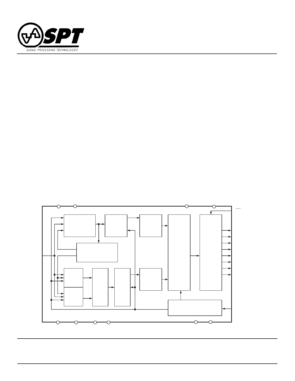
GENERAL DESCRIPTION
The SPT1175 is a CMOS two-step A/D converter capable of
digitizing full scale analog input signals into 8-bit digital words
at a sample rate of 20 MSPS.
For most applications, no external sample-and-hold or
video driving amplifiers are required due to the device's
narrow aperture time, wide bandwidth, and low input capacitance.
BLOCK DIAGRAM
RB
V
RBS
V
APPLICATIONS
• Video Digitizing
• Image Scanners
• Personal Computer Video
• Medical Ultrasound
• Multimedia
• Digital Television
The SPT1175 operates from a single +5.0 V power supply
and has an internal voltage reference which eliminates the
need for external reference circuitry. All digital inputs are
CMOS compatible and the tri-state outputs are TTL-compatible. The SPT1175 is ideal for most video and image processing applications that require low power dissipation and
low cost. The SPT1175 is available in 24-lead plastic SOIC,
plastic DIP, and PLCC packages over the commercial temperature range (0 to +70 °C). It is also available in die form.
DV
DD
DGND
OE
Coarse
Sampling
Amplifier
Fine
Fine
V
RTS
Reference Matrix
Analog
Mux
AGND
V
IN
Sampling
Amplifier
Sampling
Amplifier
V
RT
AV
Latch
Latch
D
Encoder
Encoder
Error
Correction
Circuit
Timing
Generator
DV
DD
Data
Latches
and
3-State
Output
Buffer
AGND
DØ (LSB)
D1
D2
D3
D4
D5
D6
D7 (MSB)
CLK
Signal Processing Technologies, Inc.
4755 Forge Road, Colorado Springs, Colorado 80907, USA
Phone: (719) 528-2300 FAX: (719) 528-2370
Page 2

ABSOLUTE MAXIMUM RATINGS (Beyond which damage may occur)
(1)
25 °C
Supply Voltages
VDD........................................................... -0.5 to +7.0 V
Input Voltages
Analog Input.............................................. AGND to V
Reference Input Voltage ........................... AGND to V
(2)
ESD Susceptibility
.................................................
±1,500 V
DD
DD
Temperature
Operating Temperature ................................. 0 to +70 °C
Junction Temperature ........................................... 175 °C
Lead Temperature, (soldering 10 seconds).......... 300 °C
Storage Temperature................................-55 to +125 °C
Notes: 1. Operation at any Absolute Maximum Rating is not implied. See Electrical Specifications for proper nominal
applied conditions in typical applications.
2. 100 pF discharged through a 1.5 kΩ resistor (human body model).
ELECTRICAL SPECIFICATIONS
TA= +25 °C, AVDD=DVDD=+5.0 V, AGND=DGND=0.0 V, VRB=+0.6 V and VRT=+2.6 V, unless otherwise specified.
TEST TEST SPT1175
PARAMETERS CONDITIONS LEVEL MIN TYP MAX UNITS
Resolution 8 Bits
DC Accuracy (+25 °C)
Integral Nonlinearity I ±0.8 ±1.2 LSB
Differential Nonlinearity I ±0.6 ±1.0 LSB
No Missing Codes I Guaranteed
Analog Input
Input Voltage Range I V
Input Bias Current I ±5.0 µA
Input Resistance VI 100 200 kΩ
Input Capacitance V 15 pF
Input Bandwidth V 12 MHz
Reference Input
Reference Ladder Resistance I 200 300 400 Ω
Reference Current I 5.0 6.7 10.0 mA
Reference Input Voltage V
Internal Bias V
Offset Voltage Error
Top I -18 -25 -68 mV
Bottom I 0 10 40 mV
Timing Characteristics
Maximum Conversion Rate 1 MHz Input Sine Wave I 20 30 MSPS
Output Data Delay (td) IV 18 30 ns
Output Data Delay (High Z) IV 100 ns
(Tdish, Tdisl)
Data Valid Time Tri-State Circuit IV 100 ns
(Teneh, Tenel)
Sampling Time Offset IV 5 10 ns
RB
V
RT
RB
VRT-V
RB
Short VRT and V
Short VRB and V
RTS
RBS
IV 0 0.6 - V
IV - 2.6 2.8 V
I 0.55 0.60 0.65 V
I 1.9 2.0 2.1 V
RB
V
RT
V
NOTE: It is strongly recommended that all of the supply pins (AVDD, DVDD) be powered from the same source.
SPT
2 6/24/97
SPT1175
Page 3

ELECTRICAL SPECIFICATIONS
TA=+25 °C, AVDD=DVDD=+5.0 V, AGND=DGND=0.0 V, VRB=+0.6 V and VRT=+2.6 V, unless otherwise specified.
TEST TEST SPT1175
PARAMETERS CONDITIONS LEVEL MIN TYP MAX UNITS
Dynamic Performance
Signal-To-Noise Ratio f
fIN=1.0 MHz I 44 46 dB
fIN=3.58 MHz I 43 45 dB
fIN=10 MHz V 39 dB
Spurious Free
Dynamic Range fS= 20 MSPS
fIN=1.0 MHz I 44 47 dB
fIN=3.58 MHz I 41 44 dB
fIN=10 MHz V 33 dB
Differential Phase NTSC 20 IRE Mod Ramp V 0.7 Degrees
Differential Gain fS = 14.3 MSPS V 1.0 %
Digital Inputs
Input Current, Logic High V
Input Current, Logic Low VDD = 5.25 V, VIL = DGND I 1.0 µA
Pulse Width High (CLK) IV 15 ns
Pulse Width Low (CLK) IV 15 ns
Voltage, Logic High I 4.0 V
Voltage, Logic Low I 1.0 V
Digital Outputs
Output Current, High VDD = 4.75 V IV -1.1 mA
Output Current, Low VDD = 4.75 V IV 3.5 mA
Output Current, High Z VDD = 5.25 V, OE= V
Voltage High I 4.0 V
Voltage Low I 0.4 V
Power Supply Requirements
Analog Supply Voltage (AVDD) IV +4.75 +5.0 +5.25 V
Digital Supply Voltage (DVDD) IV +4.75 +5.0 +5.25 V
Supply Voltage Difference (AVDD -DVDD) IV -0.1 0.0 0.1 V
Supply Current fS=20 MSPS I 18 27 mA
Power Dissipation I 90 135 mW
= 20 MSPS
S
= 5.25 V, VIH = V
DD
DD
DD
I 1.0 µA
IV 16 µA
TEST LEVEL CODES
All electrical characteristics are subject to the following
conditions:
All parameters having min/max specifications are guaranteed. The Test Level column indicates the specific
device testing actually performed during production
and Quality Assurance inspection. Any blank section in
the data column indicates that the specification is not
tested at the specified condition.
SPT
TEST LEVEL
I
II
III
IV
V
VI
3 6/24/97
TEST PROCEDURE
100% production tested at the specified temperature.
100% production tested at TA = +25 °C, and sample tested
at the specified temperatures.
QA sample tested only at the specified temperatures.
Parameter is guaranteed (but not tested) by design and
characterization data.
Parameter is a typical value for information purposes only.
100% production tested at T
guaranteed over specified temperature range.
= +25 °C. Parameter is
A
SPT1175
Page 4

Table I - Output Coding
INDEX ANALOG INPUT (V) OUTPUT
0 0.6078125 00000000
1 0.6078125 ~ 0.6156260 00000001 VRB=0.6 V
2 0.6156250 ~ 0.6234375 00000010 VRT=2.6 V
.... .... ....
123 1.5921875 ~ 1.6000000 01111111 1 LSB=7.8125 mV
124 1.6000000 ~ 1.6078125 10000000
125 1.6078125 ~ 1.6156250 10000001
.... .... ....
254 2.5843750 ~2.5921875 11111110
255 2.5921875 ~ 11111111
DIGITAL
Figure 1A: Timing Diagram
V
IN
Clock
Data
Figure 1B: Tri-State Output Timing Diagram
2.5 V
220 Ω
VIN (n)
Data (n-3) Data (n-2) Data (n-1) Data (n)
V
OE
OL
50%
VIN (n+1)
90%
2.5 V
TdisL
VIN (n+2)
t
d
OE
2.5 V
VIN (n+3)
50%
10%
90%
V
OL
TeneL
SPT
DUT
50 pF
OE
V
OH
50%
10%
2.5 V
TdisH
4 6/24/97
OE
2.5 V
50%
90%
V
OH
TeneH
SPT1175
Page 5

TYPICAL INTERFACE CIRCUIT
The SPT1175 is an 8-bit analog-to-digital converter which
uses a two-step, ping-pong architecture to perform conversions up to 20 MSPS. Figure 2 shows the typical interface
requirements when using the SPT1175 in normal operation.
The following sections describe the function and operation of
the device.
POWER SUPPLIES AND GROUNDING
The SPT1175 operates from a single +5 V power supply.
AVDD and DVDD must be supplied from the same source
(analog +5 V) to prevent a latch-up condition due to power
supply sequencing. Each power supply pin should be bypassed as closely as possible to the device. For optimal
performance, both the AGND and DGND should be connected to the system's analog ground plane.
ANALOG INPUT AND VOLTAGE REFERENCE
The SPT1175 input voltage range is VRT>VIN>VRB. Two
reference voltages (VRT and VRB) are required for device
operation. These voltages may be generated externally or
the SPT1175's internal reference may be used.
Inside the SPT1175, reference resistors are placed between
AVDD and V
and V
RBS
tively. (See figure 3.) In order to utilize the internal self-bias
reference voltage, V
and between AGND and V
RTS
RBS
so that V
RTS
generate the 2.6 V and 0.6 V references respec-
is to be shorted with V
RTS
RT
and the
V
pin is to be shorted to the VRB pin. The self-bias internal
RBS
reference is not as stable over temperature and supply
variations as externally generated reference voltages but will
perform well in many commercial video applications.
Figure 3 - Reference Circuit Diagram
SPT1175
AV
DD
5.0V
V
V
V
RTS
RT
RB
V
RBS
2.6 V 0.6 V
DIGITAL INPUTS AND OUTPUTS
The analog input is sampled and tracked on the first 'H' cycle
of the external clock and is held from the falling edge of CLK.
The output remains valid (output hold time), and the new data
becomes valid (output delay time) after the rising edge of
CLK, delayed by 2.5 clock cycles. The clock input and output
enable input must be driven at CMOS-compatible levels.
EVALUATION BOARD
The EB1175 evaluation board is available to aid designers in
demonstrating the full performance of the SPT1175. This
board includes a reference circuit, clock driver circuit, output
data latches, and an on-board reconstruction DAC. An application note describing the operation of the board is available.
Contact the factory for price and delivery.
AGND
0 V
Figure 2 - Typical Interface Circuit
+5
750R1R9
U1=Eleantec, EL2030
U2=OP.07
D1=D2=RCA, SK9091
Q1=Q2=2N2222A
FR=FairRite, 2743001111
All capacitors are 0.01 µF unless
otherwise specified.
R10
+5
+15
10
_
+
C59
U2
-15
GND
10
10
+
+
10
+
+
+15
-15
+5
-15
+15
C28
C29
4
+
3
U1
_
2
R37
750
R15
6
10
C8
-15
+15
FB
GND
+5 V
7
+5 V
D1
D2
C61
R8
-5
+5
Q2
750
13
DV
DD
14
AV
DD
15
AV
DD
16
V
RTS
17
V
RT
18
AV
DD
19
V
IN
20
AGND
21
AGND
22
V
RBS
23
V
RB
24
R13
2k
R2
DGND
200
CLK
DV
DD
D7
D6
D5
D4
D3
D2
D1
D0
DGND
OE
12
11
10(MSB)
9
8
7
6
5
4
3 (LSB)
2
1
EN
-5
-5
2k
Q1
V
IN
R6
75
R35
750
R36
2
10 k
3
C58
7.5 k
C60
-15
NOTE: AVDD and DVDD must be supplied from the same source (Analog +5 V)
to prevent a latch-up condition due to power supply sequencing.
Outputs
3-ST
+5
SPT
SPT1175
5 6/24/97
Page 6

PACKAGE OUTLINES
24-Lead Plastic DIP
INCHES MILLIMETERS
A 0.130 0.230 3.30 5.84
B 0.115 0.200 2.92 5.08
C 0.014 0.023 0.36 0.58
D 0.045 0.070 1.14 1.78
E .100 typ 2.54 0.00
F 0.008 0.015 0.20 0.38
G 0.115 0.195 2.92 4.95
H .30 typ 7.62 0.00
I 0.240 0.310 6.10 7.87
J 1.180 1.285 29.97 32.64
K .005 typ 0.13
24
1
K
SYMBOL MIN MAX MIN MAX
I
J
H
A
B
C
D
E
F
G
B
24
1
A
CD
24-Lead SOIC
I H
F
E
INCHES MILLIMETERS
SYMBOL MIN MAX MIN MAX
A 0.587 0.606 14.90 15.40
B
C .050 typ 1.27 typ
D 0.014 0.022 0.35 0.55
E 0.006 0.012 0.15 0.30
F 0.067 0.089 1.70 2.25
G 0.012 0.028 0.30 0.70
H 0.295 0.327 7.50 8.30
I 0.205 0.220 5.20 5.60
G
SPT
SPT1175
6 6/24/97
Page 7

PACKAGE OUTLINES
28-Lead PLCC
INCHES MILLIMETERS
SYMBOL MIN MAX MIN MAX
A 0.450 0.456 11.43 11.58
B 0.485 0.495 12.32 12.57
C45° 45°
D 0.165 0.175 4.19 4.45
E 0.010 0.25
F 0.022 typ .56 typ 0.00
G 0.18 typ 4.57 typ 0.00
H 0.05 typ 1.27 typ 0.00
I 0.039 0.430 0.99 10.92
C
Pin 1
TOP
VIEW
A
B
H
G
I
F
E
D
Pin 1
BOTTOM
VIEW
SPT
SPT1175
7 6/24/97
Page 8

D
PIN ASSIGNMENTS
OE
E
E
OE
DGND
DØ (LSB)
D1
D2
D3
D4
D5
D6
D7 (MSB)
DV
DD
CLK
DØ
DGND
4
3
DIP and
SOIC
OE
N/C
2
1
DGND
28
PIN FUNCTIONS
Name Function
DGND
V
RB
V
RBS
AGND
AGND
V
IN
AV
DD
V
RT
V
RTS
AV
DD
AV
DD
DV
DD
V
V
RBS
RB
26
27
DGND Digital Ground
D0 Digital Output Data (LSB)
D1-6 Digital Output Data
D7 Digital Output Data (MSB)
DV
DD
CLK CMOS Digital Clock Input
AV
DD
V
RTS
V
RT
V
IN
AGND Analog Ground
V
RBS
V
RB
Tri-State Output Enable
Tri-State When
Enable When
= DVDD,
O
= DGND
O
Digital Supply
Analog Supply
Internal Self-Biased Reference Top
Shorted with VRT (pin 17). Generates 2.6 V.
Reference Resistor Top Side
Analog Input
Internal Self-Biased Reference Bottom
Shorted with VRB (pin 23). Generates 0.6 V.
Reference Resistor Bottom Side
5
N/C
D1
6
D2
D3
7
8
D4
9
D5
10
D6
11
12
D7
PLCC
15
N/C
16
17
AV
DV
D
DD
DD
14
13
CLK
DV
DD
25 AGND
AGND22
V
23
IN
N/C22
AV
21
DD
20
V
RT
V
19
RTS
18
AV
ORDERING INFORMATION
PART NUMBER TEMPERATURE RANGE PACKAGE TYPE
SPT1175ACN 0 to +70 °C 24L Plastic Dip
SPT1175ACP 0 to +70 °C 28L PLCC
SPT1175ACS 0 to +70 °C 24L SOIC
SPT1175ACU +25 °C Die*
*See the die specification for guaranteed electrical performance.
Signal Processing Technologies, Inc. reserves the right to change products and specifications without notice. Permission is hereby expressly
granted to copy this literature for informational purposes only. Copying this material for any other use is strictly prohibited.
WARNING - LIFE SUPPORT APPLICATIONS POLICY - SPT products should not be used within Life Support Systems without the specific
written consent of SPT. A Life Support System is a product or system intended to support or sustain life which, if it fails, can be reasonably
expected to result in significant personal injury or death.
Signal Processing Technologies believes that ultrasonic cleaning of its products may damage the wire bonding, leading to device
failure. It is therefore not recommended, and exposure of a device to such a process will void the product warranty.
SPT
SPT1175
8 6/24/97
 Loading...