

Page 1
SPT1018
8-BIT, HIGH SPEED D/A CONVERTER
FEATURES
• 275 MWPS Conversion Rate - Version A
• 165 MWPS Conversion Rate - Version B
• Compatible with TDC1018 and HDAC10180
with Improved Performance
• RS-343-A Compatible
• Complete Video Controls: Sync, Blank, Bright
and Reference White (Force High)
• 10KH, 100K ECL Compatible
• Single Power Supply
• Registered Data and Video Controls
• Differential Current Outputs
• ESD Protected Data and Control Inputs
GENERAL DESCRIPTION
The SPT1018 is a monolithic 8-bit digital-to-analog converter
capable of accepting video data at a 165 or 275 MWPS rate.
Complete with video controls (Sync, Blank, Reference White
[Force High], Bright), the SPT1018 directly drives doublyterminated 50 or 75 ohm loads to standard composite video
levels. The standard set-up level is 7.5 IRE. The SPT1018 is
pin-compatible with the HDAC10180 and the TDC1018, with
APPLICATIONS
• High Resolution Color or Monochrome Raster
Graphics Displays
• Medical Electronics: CAT, PET, MR Imaging Displays
• CAD/CAE Workstations
• Solids Modeling
• General Purpose High-Speed D/A Conversion
• Digital Synthesizers
• Automated Test Equipment
• Digital Transmitters/Modulators
improved performance. The SPT1018 contains data and
control input registers, video control logic, reference buffer,
and current switches.
The SPT1018 is available in a 24-lead PDIP package in the
industrial temperature range. Contact the factory for military
temperature and /883 versions.
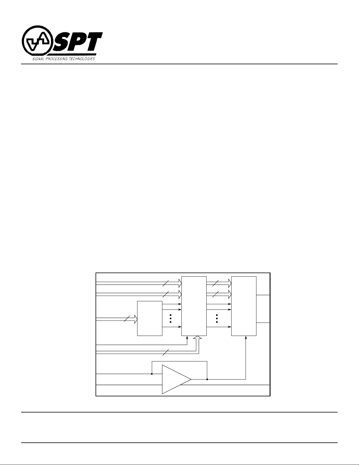
BLOCK DIAGRAM
Video Controls In
Video Data In
Video Data In
Feedthrough
Signal Processing Technologies, Inc.
Convert
Ref+
Ref-
Sync, Blank, Bright, Ref - High
D0 - D3
D4 - D7
(MSBs)
4
4
Register
4 To 15
Decode
4
2
Ref
Buffer
4
4
Output
Current
Switches
4755 Forge Road, Colorado Springs, Colorado 80907, USA
Phone: (719) 528-2300 FAX: (719) 528-2370
Out +
Out -
Comp
Page 2
ABSOLUTE MAXIMUM RATING (Beyond which damage may occur)
1
Supply Voltages
VEE (measured to VCC) ............................... -7.0 to 0.5 V
Input Voltages
CONV, Data, and Controls .......................... VEE to 0.5 V
(measured to VCC)
Temperature
Operating, ambient ................................-25 to +85 °C
junction......................................... +175 °C
Lead, Soldering (10 seconds)............................. +300 °C
Storage .....................................................-60 to +150 °C
Ref+ (measured to VCC) ..............................VEE to 0.5 V
Ref- (measured to VCC)............................... VEE to 0.5 V
Note: 1. Operation at any Absolute Maximum Ratings is not implied. See Electrical Specifications for proper nominal applied
conditions in typical applications.
ELECTRICAL SPECIFICATIONS
VCC =ground, VEE = -5.2 V ±0.3 V, TA =T
PARAMETERS CONDITIONS LEVEL MIN TYP MAX UNITS
DC ELECTRICAL CHARACTERISTICS
Integral Linearity Error 1.0 mA<I
Differential Linearity Error 1.0 mA<I
Gain Error VI -6.5 +6.5 % Full Scale
Gain Error Tempco V 150 PPM/°C
Input Capacitance, REF+, REF- V 5 pF
Compliance Voltage, +Output VI -1.2 1.5 V
Compliance Voltage, -Output VI -1.2 1.5 V
Equivalent Output Resistance VI 20 kΩ
Output Capacitance V 12 pF
Maximum Current, + Output IV 45 mA
Maximum Current, - Output IV 45 mA
Output Offset Current VI 0.05 0.5 LSB
Input Voltage, Logic HIGH VI -1.0 V
Input Voltage, Logic LOW VI -1.5 V
Convert Voltage, IV -0.5 -2.5 V
Common Mode Range (V
Convert Voltage, Differential (V
Input Current, Logic LOW, VI 35 120 µA
Data and Controls
Input Current, Logic HIGH, VI 40 120 µA
Data and Controls
Input Current, Convert VI 2 60 µA
ICM
IDF
to T
MIN
)
) IV 0.4 1.2 V
, CC = 0 pF, I
MAX
TEST TEST
<1.3 mA VI -.37 +.37 % Full Scale
Set
<1.3 mA VI -0.2 +0.2 % Full Scale
Set
= 1.105 mA, unless otherwise specified.
Set
-.95 +.95 LSB
-0.5 +0.5 LSB
SPT
SPT1018
2 5/14/97
Page 3
ELECTRICAL SPECIFICATIONS
VCC =ground, VEE = -5.2 V ±0.3 V, TA =T
PARAMETERS CONDITIONS LEVEL MIN TYP MAX UNITS
MIN
to T
TEST
, CC = 0 pF, I
MAX
= 1.105 mA, unless otherwise specified.
Set
DC ELECTRICAL CHARACTERISTICS
Input Capacitance, V 3.0 pF
Data and Controls
Power Supply Sensitivity VI -120 20 +120 µA/V
Supply Current VI 155 220 mA
DYNAMIC CHARACTERISTICS (R
Maximum Conversion Rate B Grade IV 165 MWPS
Rise Time 10% to 90% G.S. IV 1.6 ns
Rise Time 10% to 90% G.S. V 1.0 ns
Current Settling Time, Clocked Mode To 0.2% G.S. V 7.0 ns
Current Settling Time, Clocked Mode To 0.8% G.S. V 5.5 ns
Current Settling Time, Clocked Mode To 0.2% G.S. V 4.5 ns
t
SI
Clock to Output Delay, Clocked Mode IV 2.2 4.0 ns
t
DSC
Data to Output Delay, IV 3.2 6.0 ns
Transparent Mode t
Convert Pulse Width, ( Low or High) B Grade IV 3.0 ns
t
, t
PWL
PWH
Glitch Energy Area = 1/2 VT V 4 pV-s
Reference Bandwidth, -3 dB V 1.0 MHz
Set-up Time, Data and Controls IV 1.0 ns
t
S
Hold Time, Data and Controls IV 0.5 ns
t
H
Slew Rate 20% to 80% G.S. IV 390 V/µS
Clock Feedthrough IV -48 dB
DST
= 37.5 ohms, CL = 5 pF, TA = 25 °C, I
L
A Grade IV 275 MWPS
TA = T
RL = 25 ohms
RL = 25 Ω
TA = T
TA = T
A Grade IV 1.8 ns
TA = T
TA = T
TA = T
TA = T
MIN
MIN
MIN
MIN
MIN
MIN
MIN
to T
to T
to T
to T
to T
to T
to T
MAX
MAX
MAX
MAX
MAX
MAX
MAX
= 1.105 mA)
Set
IV 2.0 ns
IV 4.5 ns
IV 6.0 ns
IV 1.0 ns
IV 0.5 ns
IV 325 V/µS
IV -48 dB
TEST LEVEL CODES
All electrical characteristics are subject to the
following conditions: All parameters having min/
max specifications are guaranteed. The Test
Level column indicates the specific device testing actually performed during production and
Quality Assurance inspection. Any blank section in the data column indicates that the specification is not tested at the specified condition.
SPT
TEST LEVEL
I
II
III
IV
V
VI
3 5/14/97
TEST PROCEDURE
100% production tested at the specified temperature.
100% production tested at TA = +25 °C, and sample
tested at the specified temperatures.
QA sample tested only at the specified temperatures.
Parameter is guaranteed (but not tested) by design
and characterization data.
Parameter is a typical value for information purposes
only.
100% production tested at TA = +25 °C. Parameter is
guaranteed over specified temperature range.
SPT1018
Page 4
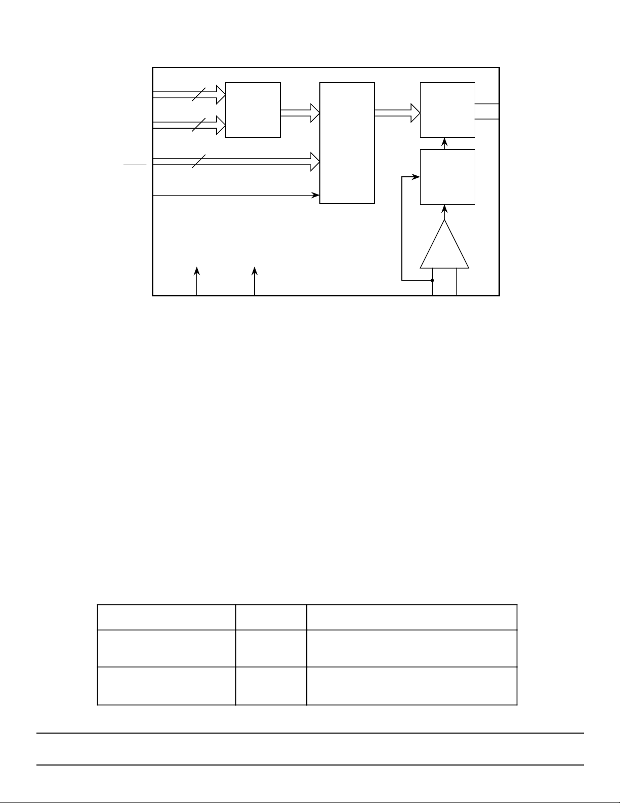
Figure 1 - Functional Diagram
D0 - D7
Composite
Video Controls
CONV
CONV
Feedthrough
8
4
2
V
EE
Decoding
Logic
V
CC Ref-
APPLICATION INFORMATION
The SPT1018 is a high speed video digital-to-analog converter capable of conversion rates of up to 275 MWPS. This
makes the device suitable for driving 1500 X 1800 pixel
displays at 70 to 90 Hz update rates.
The SPT1018 is separated into different conversion rate
categories as shown in table I.
The SPT1018 has 10 KH and 100K ECL logic level compatible video controls and data inputs. The complementary
analog output currents produced by the devices are proportional to the product of the digital control and data inputs in
conjunction with the analog reference current. The SPT1018
is segmented so that the four MSBs of the input data are
separated into a parallel thermometer code. From here,
Current
Sources
And
Switches
Data
Registers
Current
Source
Biasing
Amp
+-
Ref+
Out +
Out -
fifteen identical current sinks are driven to fabricate sixteen
coarse output levels. The remaining four LSBs drive four
binary weighted current switches.
The MSB currents are then summed with the LSBs, which
provide a one-sixteenth of full scale contribution, to provide
the 256 distinct analog output levels.
The video control inputs drive weighted current sinks that are
added to the output current to produce composite video
output levels. These controls, Sync, Blank, Reference White
(Force High), and Bright are needed in video applications.
Another feature that similar video D/A converters do not have
is the Feedthrough Control. This pin allows registered or
unregistered operation of the video control and data inputs.
In the registered mode, the composite functions are latched
to the pixel data to prevent screen-edge distortions generally
found on unregistered video DACs.
Table I - The SPT1018 Family and Speed Designations
PART NUMBER UPDATE COMMENTS
SPT1018A 275 MWPS Suitable for 1200 X 1500 to 1500 X 1800
SPT1018B 165 MWPS Suitable for 1024 X 1280 to 1200 X 1500
SPT
displays at 60 to 90 Hz update rate.
displays at 60 to 90 Hz update rate.
SPT1018
4 5/14/97
Page 5

Figure 2 - Typical Interface Circuit
FT
Data
Clock
V+
V-
.01 µF
FB
FH
Blank
BRT
Sync
D0 (LSB)
D1
D2
D3
D4
D5
D6
D7 (MSB)
CONV
CONV
I
*
Set
4 To 15
Decode
)(
Ref+
Ref-
R
1
500 Ω
LM113/313
– 5.2 V
750 Ω
I
Set
2 kΩ
R
2
1 kΩ
Video
Control
Inputs
Video
Inputs
Ref
Buffer
Video Monitor
Out-
R
3
50/75 Ω
Out+
50/75 Ω COAX
NOTES:
V- = -1.2 V (typical) for LM113.
1.
V+ = -1.2 V
2.
I
3.
Set
R
4.
V
5.
6.
V
=
α
T(R
= R3 / / R4
L
255-Digital Input Code
K
=
Out
= (K x I
Sync
V+
1+R2
Set
)
255
x RL) + (K2 x I
R
50/75 Ω
x I
Set
4
Set
R
L
+
x RL (Bright)
[]
K
x I
Set
I
x RL)
Register
4
4
Output
Current
Switches
K = 15.8069
K
= 1.7617
1
= 10.0392
K
2
7.
FB = Ferrite bead, Fair-rite P/N 217430011 or equivalent.
8.
All reference resistors 1/8 W 1% metal film
power supply decoupling 50 V ceramic disc.
9.
10.
11.
10.
= ECL Terminationx
= V
= AGND
CC
See figure 8 for detail on Ref Buffer.
= DGND (digital input drivers).
-5.2 V
V
EE
COMP
V
CC
.01 µF
10 µF
TYPICAL INTERFACE CIRCUIT
GENERAL
A typical interface circuit using the SPT1018 in a color raster
application is shown in figure 2. The SPT1018 requires few
external components and is extremely easy to use. The very
high operating speeds of the SPT1018 require good circuit
layout, decoupling of supplies, and proper design of transmission lines. The following considerations should be noted
to achieve best performance.
INPUT CONSIDERATIONS
Video input data and controls may be directly connected to
the SPT1018. Note that all ECL inputs are terminated as
closely to the device as possible to reduce ringing, crosstalk
and reflections. A convenient and commonly used microstrip
impedance is about 130 ohms, which is easily terminated
using a 330 ohm resistor to VEE and a 220 ohm resistor to
Ground. This arrangement gives a Thevenin equivalent termination of 130 ohms to -2 volts without the need for a
-2 volt supply. Standard SIP (Single Inline Package) 220/330
resistor networks are available for this purpose. It is recommended that stripline or microstrip techniques be used for all
ECL interface. Printed circuit wiring of known impedance
over a solid ground plane is recommended.
OUTPUT CONSIDERATIONS
The analog outputs are designed to directly drive a dual 50 or
75 ohm load transmission system as shown. The source
impedances of the SPT1018 outputs are high impedance
current sinks. The load impedance (RL) must be 25
or 37.5 ohms to attain standard RS-343-A video levels. Any
deviation from this impedance will affect the resulting video
output levels proportionally. As with the data interface, it is
important that the analog transmission lines have matched
impedance throughout, including connectors and transitions
between printed wiring and coaxial cable. The combination of
matched source termination resistor RS and load terminator
RL minimizes reflections of both forward and reverse traveling waves in the analog transmission system. The return path
for analog output current is V
which is connected to the
CC
source termination resistor RS.
SPT
SPT1018
5 5/14/97
Page 6

POWER CONSIDERATIONS
The SPT1018 operates from a single -5.2 V standard supply.
Proper bypassing of the supplies will augment the SPT1018’s
inherent supply noise rejection characteristics. As shown in
figure 2, each supply pin should be bypassed as close to the
device as possible with 0.01 µF and 10 µF capacitors.
The SPT1018 has two analog (VEE) power supply pins. Both
supply pins should be properly bypassed as mentioned
previously. This device also has two analog (VCC) ground
pins. Both ground pins should be tied to the analog ground
plane. Power and ground pins must be connected in all
applications. If a +5 V power source is required, the ground
pins (VCC) become the positive supply pins while the supply
pins (VEE) become the ground pins. The relative polarities of
the other input and output voltages must be maintained.
REFERENCE CONSIDERATIONS
The SPT1018 has two reference inputs: Ref+ and Ref-. These
pins are connected to the inverting and noninverting inputs of
an internal amplifier that serves as a reference buffer amplifier.
The output of the buffer amplifier is the reference for the
current sinks. The amplifier feedback loop is connected
around one of the current sinks to achieve better accuracy.
(See figure 8.)
Since the analog output currents are proportional to the digital
input data and the reference current (I
output may be adjusted by varying the reference current. I
), the full-scale
Set
Set
is controlled through the Ref+ input on the SPT1018. A
method and equations to set I
is shown in figure 2. The
Set
SPT1018 uses an external negative voltage reference. The
external reference must be stable to achieve a satisfactory
output and the Ref- pin should be driven through a resistor to
minimize offsets caused by bias current. The value for I
Set
can be varied with the 500 ohm trimmer to change the full
scale output. A double 50 ohm load (25 ohm) can be driven
if I
is increased 50% more than I
Set
for doubly terminated
Set
75 ohm video applications.
COMPENSATION
The SPT1018 provides an external compensation input
(COMP) for the reference buffer amplifier. In order to use this
pin correctly, a capacitor should be connected between
COMP and VEE as shown in figure 2. Keep the lead lengths
as short as possible. If the reference is to be kept as a
constant, use a large capacitor (.01 µF). The value of the
capacitor determines the bandwidth of the amplifier. If modulation of the reference is required, smaller values of capacitance can be used to achieve up to a 1 MHz bandwidth.
DATA INPUTS AND VIDEO CONTROLS
The SPT1018 has standard single-ended data inputs. The
inputs are registered to produce the lowest differential data
propagation delay (skew) to minimize glitching. There are
also four video control inputs to generate composite video
outputs. These are Sync, Blank, Bright and Reference White
or Force High. Also provided is the Feedthrough control as
mentioned earlier. The controls and data inputs are all 10 KH
and 100K ECL compatible. In addition, all have internal
pulldown resistors to leave them at a logic low so the pins are
inactive when not used. This is useful if the devices are
applied as standard DACs without the need for video controls
or if less than eight bits are used.
Figure 3 - Timing Diagram
SPT
CONV
-1.3 V
CONV
-1.3 V
OUT -
OUT +
t
S
Data Control
t
PWH
t
PWL
t
H
Inputs
t
DST
t
DSC
t
SI
1/2 LSB
1/2 LSB
SPT1018
6 5/14/97
Page 7

Table II - Video Control Operation (Output values for set-up = 10 IRE and 75 ohm standard load)
Sync Blank
1 X X X X 28.57 -1.071 -40 Sync Level
0 1 X X X 20.83 -0.781 0 Blank Level
0 0 1 1 X 0.00 0.000 110 Enhanced High Level
0 0 1 0 X 1.95 -0.073 100 Normal High Level
0 0 0 0 000... 19.40 -0.728 7.5 Normal Low Level
0 0 0 0 111... 1.95 -0.073 100 Normal High Level
0 0 0 1 000... 17.44 -0.654 17.5 Enhanced Low Level
0 0 0 1 111... 0.00 0.000 110 Enhanced High Level
Ref
White Bright
Data
Input Out - (mA) Out - (V) Out - (IRE) Description
The SPT1018 is usually configured in the synchronous
mode. In this mode, the controls and data are synchronized
to prevent pixel dropout. This reduces screen-edge distortions and provides the lowest output noise while maintaining
the highest conversion rate. By leaving the Feedthrough (FT)
control open (low), each rising edge of the convert (CONV)
clock latches decoded data and control values into a D-type
internal register. The registered data is then converted into
the appropriate analog output by the switched current sinks.
When FT is tied high, the control inputs and data are not
registered. The analog output asynchronously tracks the
input data and video controls. Feedthrough itself is asynchronous and usually used as a DC control.
The controls and data have to be present at the input pins for
a set-up time of ts before, and a hold time of th after, the rising
edge of the clock (CONV) in order to be synchronously
registered. The set-up and hold times are not important in the
asynchronous mode. The minimum pulse widths high (t
and low (t
) as well as settling time become the limiting
PWL
PWH
factors. (See figure 3.)
The video controls produce the output levels needed for
horizontal blanking, frame synchronization, etc., to be compatible with video system standards as described in
RS-343-A. Table II shows the video control effects on the
analog output. Internal logic governs Blank, Sync, and Force
High so that they override the data inputs as needed in video
applications. Sync overrides both the data and other controls
to produce full negative video output (figure 9).
Reference White video level output is provided by Force
High, which drives the internal digital data to full scale output
or 100 IRE units. Bright gives an additional 10% of full scale
value to the output level. This function can be used in graphic
displays for highlighting menus, cursors or warning messages. Again, if the devices are used in non-video applications, the video controls can be left open.
CONVERT CLOCK
For best performance, the clock should be ECL driven,
differentially, by utilizing CONV and
CONV
(figure 4). By
driving the clock this way, clock noise and power supply/
output intermodulation will be minimized. The rising edge of
the clock synchronizes the data and control inputs to the
SPT1018. Since the actual switching threshold of
determined by CONV, the clock can be driven single-ended
by connecting a bias voltage to
. The switching thresh-
CONV
old of CONV is set by this bias voltage.
)
ANALOG OUTPUTS
The SPT1018 has two analog outputs that are high impedance, complementary current sinks. The outputs vary in
proportion to the input data, controls and reference current
values so that the full scale output can be changed by setting
I
as mentioned earlier.
Set
In video applications, the outputs can drive a doubly terminated 50 or 75 ohm load to standard video levels. In the
standard configuration of figure 5, the output voltage is the
product of the output current and load impedance and is
between 0 and -1.07 V. The Out- output (figure 9) will provide
a video output waveform with the Sync pulse bottom at the
-1.07 V level. The Out+ is inverted with Sync up.
CONV
is
SPT
SPT1018
7 5/14/97
Page 8

Figure 4 - CONVert,
Ref-Ref+
750 Ω500 Ω
750 Ω500 Ω
R G
1 kΩ
Ref-Ref+
B
1 kΩ
Ref Out
I
Set
R
2
750 Ω
R
1
500 Ω
I
Ref
I
Set
I
Set
I
Set
SPT1019
(Master)
SPT1018
(Slave)
SPT1018
(Slave)
V
IDF
V
ICM MAX
CONVert
Figure 5A -Standard Load
Switching Levels
Video Monitor
0.0 V
V
ICM MIN
-1.3 V
CONV
CONV
external load, such as two other DAC reference inputs. (See
the SPT1019 data sheet).
The circuits shown in figure 6 illustrate how a single SPT1019
may be used as a master reference in a system with multiple
DACs (such as RGB). The other DACs are simply slaved from
the SPT1019’s reference output. The SPT1018s shown are
especially well-suited to be slaved to a SPT1019 for a better
TC tracking from DAC-to-DAC, since they are essentially
SPT1019s without the reference. The SPT1018 is pin-compatible with the TDC1018, that does not have an internal
reference. Although either the TDC1018 or the SPT1018 may
be slaved from an SPT1019, the higher performance
SPT1018 and the above mentioned DAC-to-DAC TC tracking is the best choice for new designs.
SPT1018
OUT-
OUT +
R
75 Ω
R
75 Ω
S
S
75 Ω COAX
75 Ω COAX
75 Ω
75 Ω
R
L
Inverse
Video
R
L
Figure 5B -Test Load
OUT +
OUT -
C
L
<5 pF
R
37.5Ω
L
Video Out
0 to -1 Volt
TYPICAL RGB GRAPHICS SYSTEM
In an RGB graphics system, the color displayed is determined
by the combined intensities of the red, green and blue (RGB)
D/A converter outputs. A change in gain or offset in any of the
RGB outputs will affect the apparent hue displayed on the
CRT screen.
Thus, it is very important that the outputs of the D/A converters track each other over a wide range of operating conditions. Since the D/A output is proportional to the product of the
reference and digital input code, a common reference should
be used to drive all three D/As in an RGB system to minimize
RGB DAC-to-DAC mismatch and improve TC tracking.
The SPT1019 contains an internal precision bandgap reference which completely eliminates the need for an external
reference. The reference can supply up to 50 µA to an
No external reference is required for operation of the
SPT1019, as this function is provided internally. The internal
reference is a bandgap type and is suitable for operation over
extended temperature ranges. The SPT1018 must use an
external reference.
Figure 6 - Typical RGB Graphics System
Figure 7 - Burn-In Circuit
-5.9 V
(Max 200 mA)
24 Pin DIP
All Resistors Are 5% 1/4 W cc
Clock = -0.9 to -1.7 V, 100 kHz
(Max 50 mA)
Out-
CC
Out+
Ref+
(Max 50 mA)
100 Ω
1 kΩ
(Max 1.5 mA)
100 Ω
-1.2 V
(Max 1.5 mA)
-1.3 V
(Max 60 µA)
Clock
(Max 60 µA)
1 kΩ
1 kΩ
1 kΩ
6.5 Ω
Ref-
CONV
CONV
6.5 Ω
V
EE
V
SPT
SPT1018
8 5/14/97
Page 9

I
Bias
V
EE
V
CC
Reference
Segment
Switch
Ref-
Ref+
I
Bias
I
Bias
Figure 8 - DAC Output Circuit
Reference
Amplifier
Ref+
Reference
Current
Current
Sink #1
Current
Sink #N
Out+
Out-
Ref-
+
-
Comp
Figure 9 - Video Output Waveform for Standard Load
IRE
110
100
7.5
-40
0
0 mV
-73 mV
-728 mV
-781 mV
-1071 mV
Bright
Normal High (White)
I
Seg
256 Gray Levels
Blank
Normal Low (Black)
Sync
Video
I
Seg
V
EE
Figure 10 - Equivalent Input Circuits - Data, Clock, Controls and Reference
Conv
Conv
I
Bias
V
EE
SPT
Data and
Controls
80 kΩ
I
Bias
V
EE
9 5/14/97
V
SPT1018
Page 10

24
1
PACKAGE OUTLINE
24-Lead PDIP
INCHES MILLIMETERS
SYMBOL MIN MAX MIN MAX
K
I
J
A
B
C
D
E
F
G
H
I
J
K
0.125
0.015
0.100 typ
0.055
0.008
0.150 typ
0.600
0.530
1.245
0.070
0.190
0.135
0.022
0.065
0.012
0.625
0.550
1.255
0.080
3.18
0.38
2.54 typ
1.40
0.20
3.81 typ
15.24
13.46
31.62
1.78
4.83
3.43
0.56
1.65
0.30
15.88
13.97
31.88
2.03
H
A
B
C
D
E
F
G
SPT
SPT1018
10 5/14/97
Page 11

PIN ASSIGNMENTS
1
D3
2
D2
3
D1
4
D0
EE
FT
CC
FH
5
6
7
8
9
10
11
12
V
CONV
CONV
V
Blank
BRT
PDIP
24
23
22
21
20
19
18
17
16
15
14
13
D4
D5
D6
D7
V
EE
Out +
Out V
CC
Comp
Ref+
RefSync
PIN FUNCTIONS
Name Function
D3 Data Bit 3
D2 Data Bit 2
D1 Data Bit 1
D0 Data Bit 0 (LSB)
V
EE
CONV Convert Clock Input
CONV
FT Register Feedthrough Control
V
CC
FH Data Force High Control
Blank Video Blank Input
BRT Video Bright Input
Sync Video Sync Input
Ref- Reference Current - Input
Ref+ Reference Current + Input
COMP Compensation Input
Out- Output Current Negative
Out+ Output Current Positive
D7 Data Bit 7 (MSB)
D6 Data Bit 6
D5 Data Bit 5
D4 Data Bit 4
Negative Supply
Convert Clock Input Complement
Positive Supply
ORDERING INFORMATION
PART NUMBER DESCRIPTION TEMPERATURE RANGE PACKAGE
SPT1018AIN 8-BIT, 275 MWPS DAC -25 to +85 °C 24L PDIP
SPT1018BIN 8-BIT, 165 MWPS DAC -25 to +85 °C 24L PDIP
Signal Processing Technologies, Inc. reserves the right to change products and specifications without notice. Permission is hereby expressly
granted to copy this literature for informational purposes only. Copying this material for any other use is strictly prohibited.
WARNING - LIFE SUPPORT APPLICATIONS POLICY - SPT products should not be used within Life Support Systems without the specific
written consent of SPT. A Life Support System is a product or system intended to support or sustain life which, if it fails, can be reasonably
expected to result in significant personal injury or death.
Signal Processing Technologies believes that ultrasonic cleaning of its products may damage the wire bonding, leading to device
failure. It is therefore not recommended, and exposure of a device to such a process will void the product warranty.
SPT1018
SPT
11 5/14/97
 Loading...