

Low data rate, low power sub-1GHZ transceiver
QFN20
Features
■ Frequency bands: 150-174 MHz, 300-348
MHz, 387-470 MHz, 779-956 MHz
■ Modulation schemes: 2-FSK, GFSK, MSK,
GMSK, OOK, and ASK
■ Air data rate from 1 to 500 kbps
■ Very low power consumption (9 mA RX and 21
mA TX at +11 dBm)
■ Programmable RX digital filter from 6 kHz to
800 kHz
■ Programmable channel spacing (12.5 kHz
min.)
■ Excellent performance of receiver sensitivity (-
120 dBm), selectivity, and blocking
■ Programmable output power up to +11 dBm
■ Fast startup and frequency synthesizer settling
time (6 µs)
■ Frequency offset compensation
■ Integrated temperature sensor
■ Battery indicator and low battery detector
■ RX and TX FIFO buffer (96 bytes each)
■ Configurability via SPI interface
■ Automatic acknowledgement, retransmission,
and timeout protocol engine
■ AES 128-bit encryption co-processor
■ Antenna diversity algorithm
■ Fully integrated ultra low power RC oscillator
■ Wake-up on internal timer and wake-up on
external event
■ Flexible packet length with dynamic payload
length
■ Sync word detection
■ Address check
■ Automatic CRC handling
■ FEC with interleaving
SPIRIT1
Datasheet — preliminary data
■ Digital RSSI output
■ Programmable carrier sense (CS) indicator
■ Automatic clear channel assessment (CCA)
before transmitting (for listen-before-talk
systems). Embedded CSMA/CA protocol
■ Programmable preamble quality indicator
(PQI)
■ Link quality indication (LQI)
■ Whitening and de-whitening of data
■ Wireless M-BUS, EN 300 220, FCC CFR47 15
(15.205, 15.209, 15.231, 15.247, 15.249), and
ARIB STD T-67, T93, T-108 compliant
■ QFN20 4x4 mm RoHS package
■ Operating temperature range from -40 °C to 85
°C
Applications
■ AMR (automatic meter reading)
■ Home and building automation
■ WSN (wireless sensors network)
■ Industrial monitoring and control
■ Wireless fire and security alarm systems
■ Point-to-point wireless link
Table 1. Device summary
Order code Package Packing
SPIRIT1QTR QFN20 Tape and reel
April 2012 Doc ID 022758 Rev 2 1/91
This is preliminary information on a new product now in development or undergoing evaluation. Details are subject to
change without notice.
www.st.com
91

Contents SPIRIT1
Contents
1 Description . . . . . . . . . . . . . . . . . . . . . . . . . . . . . . . . . . . . . . . . . . . . . . . . . 5
2 Introduction . . . . . . . . . . . . . . . . . . . . . . . . . . . . . . . . . . . . . . . . . . . . . . . . 6
3 Typical application diagram and pin description . . . . . . . . . . . . . . . . . . 8
3.1 Typical application diagram . . . . . . . . . . . . . . . . . . . . . . . . . . . . . . . . . . . . 8
4 Pinout . . . . . . . . . . . . . . . . . . . . . . . . . . . . . . . . . . . . . . . . . . . . . . . . . . . . 10
5 Absolute maximum ratings and thermal data . . . . . . . . . . . . . . . . . . . 11
6 Characteristics . . . . . . . . . . . . . . . . . . . . . . . . . . . . . . . . . . . . . . . . . . . . 12
6.1 General characteristics . . . . . . . . . . . . . . . . . . . . . . . . . . . . . . . . . . . . . . . 12
6.2 Electrical specifications . . . . . . . . . . . . . . . . . . . . . . . . . . . . . . . . . . . . . . 12
6.2.1 Electrical characteristics . . . . . . . . . . . . . . . . . . . . . . . . . . . . . . . . . . . . 12
6.2.2 Digital SPI . . . . . . . . . . . . . . . . . . . . . . . . . . . . . . . . . . . . . . . . . . . . . . . 13
6.2.3 RF receiver . . . . . . . . . . . . . . . . . . . . . . . . . . . . . . . . . . . . . . . . . . . . . . 14
6.2.4 RF transmitter . . . . . . . . . . . . . . . . . . . . . . . . . . . . . . . . . . . . . . . . . . . . 17
6.2.5 Crystal oscillator . . . . . . . . . . . . . . . . . . . . . . . . . . . . . . . . . . . . . . . . . . 21
6.2.6 Sensors . . . . . . . . . . . . . . . . . . . . . . . . . . . . . . . . . . . . . . . . . . . . . . . . . 22
7 Operating modes . . . . . . . . . . . . . . . . . . . . . . . . . . . . . . . . . . . . . . . . . . . 24
7.1 Reset sequence . . . . . . . . . . . . . . . . . . . . . . . . . . . . . . . . . . . . . . . . . . . . 27
7.2 Timer usage . . . . . . . . . . . . . . . . . . . . . . . . . . . . . . . . . . . . . . . . . . . . . . . 28
7.3 Low duty cycle reception mode . . . . . . . . . . . . . . . . . . . . . . . . . . . . . . . . 28
7.4 CSMA/CA engine . . . . . . . . . . . . . . . . . . . . . . . . . . . . . . . . . . . . . . . . . . . 29
8 Block description . . . . . . . . . . . . . . . . . . . . . . . . . . . . . . . . . . . . . . . . . . 33
8.1 Power management . . . . . . . . . . . . . . . . . . . . . . . . . . . . . . . . . . . . . . . . . 33
8.2 Power-on-reset (POR) . . . . . . . . . . . . . . . . . . . . . . . . . . . . . . . . . . . . . . . 33
8.3 Low battery indicator . . . . . . . . . . . . . . . . . . . . . . . . . . . . . . . . . . . . . . . . 33
8.4 Voltage reference . . . . . . . . . . . . . . . . . . . . . . . . . . . . . . . . . . . . . . . . . . . 33
8.5 Oscillator and RF synthesizer . . . . . . . . . . . . . . . . . . . . . . . . . . . . . . . . . 33
8.6 RCO: features and calibration . . . . . . . . . . . . . . . . . . . . . . . . . . . . . . . . . 36
2/91 Doc ID 022758 Rev 2

SPIRIT1 Contents
8.6.1 RC oscillator calibration . . . . . . . . . . . . . . . . . . . . . . . . . . . . . . . . . . . . . 36
8.7 AFC . . . . . . . . . . . . . . . . . . . . . . . . . . . . . . . . . . . . . . . . . . . . . . . . . . . . . 37
8.8 Receiver . . . . . . . . . . . . . . . . . . . . . . . . . . . . . . . . . . . . . . . . . . . . . . . . . . 37
8.9 Transmitter . . . . . . . . . . . . . . . . . . . . . . . . . . . . . . . . . . . . . . . . . . . . . . . . 37
8.10 Temperature sensors (TS) . . . . . . . . . . . . . . . . . . . . . . . . . . . . . . . . . . . . 38
8.11 AES encryption co-processor . . . . . . . . . . . . . . . . . . . . . . . . . . . . . . . . . . 38
9 Transmission and reception . . . . . . . . . . . . . . . . . . . . . . . . . . . . . . . . . . 40
9.1 PA configuration . . . . . . . . . . . . . . . . . . . . . . . . . . . . . . . . . . . . . . . . . . . . 40
9.2 RF channel frequency settings . . . . . . . . . . . . . . . . . . . . . . . . . . . . . . . . . 41
9.3 RX timeout management . . . . . . . . . . . . . . . . . . . . . . . . . . . . . . . . . . . . . 43
9.4 Intermediate frequency setting . . . . . . . . . . . . . . . . . . . . . . . . . . . . . . . . . 44
9.5 Modulation scheme . . . . . . . . . . . . . . . . . . . . . . . . . . . . . . . . . . . . . . . . . 45
9.5.1 Data rate . . . . . . . . . . . . . . . . . . . . . . . . . . . . . . . . . . . . . . . . . . . . . . . . 47
9.5.2 RX channel bandwidth . . . . . . . . . . . . . . . . . . . . . . . . . . . . . . . . . . . . . . 47
9.6 Data coding and integrity check process . . . . . . . . . . . . . . . . . . . . . . . . . 48
9.6.1 FEC . . . . . . . . . . . . . . . . . . . . . . . . . . . . . . . . . . . . . . . . . . . . . . . . . . . . 48
9.6.2 CRC . . . . . . . . . . . . . . . . . . . . . . . . . . . . . . . . . . . . . . . . . . . . . . . . . . . . 48
9.6.3 Data whitening . . . . . . . . . . . . . . . . . . . . . . . . . . . . . . . . . . . . . . . . . . . . 49
9.6.4 Data padding . . . . . . . . . . . . . . . . . . . . . . . . . . . . . . . . . . . . . . . . . . . . . 49
9.7 Packet handler engine . . . . . . . . . . . . . . . . . . . . . . . . . . . . . . . . . . . . . . . 50
9.7.1 STack packet . . . . . . . . . . . . . . . . . . . . . . . . . . . . . . . . . . . . . . . . . . . . . 50
9.7.2 Wireless M-Bus packet (W M-BUS, EN13757-4) . . . . . . . . . . . . . . . . . . 51
9.7.3 Basic packet . . . . . . . . . . . . . . . . . . . . . . . . . . . . . . . . . . . . . . . . . . . . . . 52
9.7.4 Automatic packet filtering . . . . . . . . . . . . . . . . . . . . . . . . . . . . . . . . . . . . 53
9.7.5 Link layer protocol . . . . . . . . . . . . . . . . . . . . . . . . . . . . . . . . . . . . . . . . . 54
9.8 Data modes . . . . . . . . . . . . . . . . . . . . . . . . . . . . . . . . . . . . . . . . . . . . . . . 55
9.9 Data FIFO . . . . . . . . . . . . . . . . . . . . . . . . . . . . . . . . . . . . . . . . . . . . . . . . . 56
9.10 Receiver quality indicators . . . . . . . . . . . . . . . . . . . . . . . . . . . . . . . . . . . . 58
9.10.1 RSSI . . . . . . . . . . . . . . . . . . . . . . . . . . . . . . . . . . . . . . . . . . . . . . . . . . . 58
9.10.2 Carrier sense . . . . . . . . . . . . . . . . . . . . . . . . . . . . . . . . . . . . . . . . . . . . . 58
9.10.3 LQI . . . . . . . . . . . . . . . . . . . . . . . . . . . . . . . . . . . . . . . . . . . . . . . . . . . . . 59
9.10.4 PQI . . . . . . . . . . . . . . . . . . . . . . . . . . . . . . . . . . . . . . . . . . . . . . . . . . . . . 59
9.10.5 SQI . . . . . . . . . . . . . . . . . . . . . . . . . . . . . . . . . . . . . . . . . . . . . . . . . . . . . 59
9.11 Antenna diversity . . . . . . . . . . . . . . . . . . . . . . . . . . . . . . . . . . . . . . . . . . . 60
Doc ID 022758 Rev 2 3/91

Contents SPIRIT1
9.12 Frequency hopping . . . . . . . . . . . . . . . . . . . . . . . . . . . . . . . . . . . . . . . . . . 61
10 MCU interface . . . . . . . . . . . . . . . . . . . . . . . . . . . . . . . . . . . . . . . . . . . . . 62
10.1 Serial peripheral interface . . . . . . . . . . . . . . . . . . . . . . . . . . . . . . . . . . . . 62
10.2 Interrupts . . . . . . . . . . . . . . . . . . . . . . . . . . . . . . . . . . . . . . . . . . . . . . . . . 64
10.3 GPIOs . . . . . . . . . . . . . . . . . . . . . . . . . . . . . . . . . . . . . . . . . . . . . . . . . . . 65
10.4 MCU clock . . . . . . . . . . . . . . . . . . . . . . . . . . . . . . . . . . . . . . . . . . . . . . . . 67
11 Register table . . . . . . . . . . . . . . . . . . . . . . . . . . . . . . . . . . . . . . . . . . . . . . 69
12 Package mechanical data . . . . . . . . . . . . . . . . . . . . . . . . . . . . . . . . . . . . 86
13 Revision history . . . . . . . . . . . . . . . . . . . . . . . . . . . . . . . . . . . . . . . . . . . 88
4/91 Doc ID 022758 Rev 2

SPIRIT1 List of tables
List of tables
Table 1. Device summary . . . . . . . . . . . . . . . . . . . . . . . . . . . . . . . . . . . . . . . . . . . . . . . . . . . . . . . . . . 1
Table 2. Description of the external components of the typical application diagram . . . . . . . . . . . . . 8
Table 3. Pinout description . . . . . . . . . . . . . . . . . . . . . . . . . . . . . . . . . . . . . . . . . . . . . . . . . . . . . . . . 10
Table 4. Absolute maximum ratings . . . . . . . . . . . . . . . . . . . . . . . . . . . . . . . . . . . . . . . . . . . . . . . . . 11
Table 5. Thermal data. . . . . . . . . . . . . . . . . . . . . . . . . . . . . . . . . . . . . . . . . . . . . . . . . . . . . . . . . . . . 11
Table 6. Recommended operating conditions . . . . . . . . . . . . . . . . . . . . . . . . . . . . . . . . . . . . . . . . . 11
Table 7. General characteristics . . . . . . . . . . . . . . . . . . . . . . . . . . . . . . . . . . . . . . . . . . . . . . . . . . . . 12
Table 8. Power consumption . . . . . . . . . . . . . . . . . . . . . . . . . . . . . . . . . . . . . . . . . . . . . . . . . . . . . . 13
Table 9. Digital SPI input and output (SDO, SDI, SCLK, CSn, and SDN) and GPIO specification
(GPIO_1-4) . . . . . . . . . . . . . . . . . . . . . . . . . . . . . . . . . . . . . . . . . . . . . . . . . . . . . . . . . . . . . 13
Table 10. RF receiver characteristics . . . . . . . . . . . . . . . . . . . . . . . . . . . . . . . . . . . . . . . . . . . . . . . . . 14
Table 11. RF transmitter characteristics . . . . . . . . . . . . . . . . . . . . . . . . . . . . . . . . . . . . . . . . . . . . . . . 17
Table 12. Crystal oscillator characteristics . . . . . . . . . . . . . . . . . . . . . . . . . . . . . . . . . . . . . . . . . . . . . 21
Table 13. Ultra low power RC oscillator . . . . . . . . . . . . . . . . . . . . . . . . . . . . . . . . . . . . . . . . . . . . . . . 22
Table 14. N-Fractional ÓÄ frequency synthesizer characteristics . . . . . . . . . . . . . . . . . . . . . . . . . . . 22
Table 15. Analog temperature sensor characteristics . . . . . . . . . . . . . . . . . . . . . . . . . . . . . . . . . . . . 22
Table 16. Battery indicator and low battery detector . . . . . . . . . . . . . . . . . . . . . . . . . . . . . . . . . . . . . 23
Table 17. States . . . . . . . . . . . . . . . . . . . . . . . . . . . . . . . . . . . . . . . . . . . . . . . . . . . . . . . . . . . . . . . . . 25
Table 18. Commands list . . . . . . . . . . . . . . . . . . . . . . . . . . . . . . . . . . . . . . . . . . . . . . . . . . . . . . . . . . 26
Table 19. POR parameters . . . . . . . . . . . . . . . . . . . . . . . . . . . . . . . . . . . . . . . . . . . . . . . . . . . . . . . . . 28
Table 20. SPIRIT1 timers description and duration . . . . . . . . . . . . . . . . . . . . . . . . . . . . . . . . . . . . . . 28
Table 21. Programmability of trans-conductance at startup . . . . . . . . . . . . . . . . . . . . . . . . . . . . . . . . 34
Table 22. CP word look-up . . . . . . . . . . . . . . . . . . . . . . . . . . . . . . . . . . . . . . . . . . . . . . . . . . . . . . . . . 35
Table 23. PA_level . . . . . . . . . . . . . . . . . . . . . . . . . . . . . . . . . . . . . . . . . . . . . . . . . . . . . . . . . . . . . . . 40
Table 24. Frequency threshold . . . . . . . . . . . . . . . . . . . . . . . . . . . . . . . . . . . . . . . . . . . . . . . . . . . . . . 43
Table 25. RX timeout stop condition configuration . . . . . . . . . . . . . . . . . . . . . . . . . . . . . . . . . . . . . . . 43
Table 26. IF_OFFSET settings . . . . . . . . . . . . . . . . . . . . . . . . . . . . . . . . . . . . . . . . . . . . . . . . . . . . . . 45
Table 27. CHFLT_M and CHFLT_E value for channel filter bandwidth (in kHz, for fclk = 26 MHz) . . 47
Table 28. Packet configuration . . . . . . . . . . . . . . . . . . . . . . . . . . . . . . . . . . . . . . . . . . . . . . . . . . . . . . 54
Table 29. MCU clock vs. state . . . . . . . . . . . . . . . . . . . . . . . . . . . . . . . . . . . . . . . . . . . . . . . . . . . . . . 64
Table 30. Interrupts. . . . . . . . . . . . . . . . . . . . . . . . . . . . . . . . . . . . . . . . . . . . . . . . . . . . . . . . . . . . . . . 64
Table 31. Digital outputs . . . . . . . . . . . . . . . . . . . . . . . . . . . . . . . . . . . . . . . . . . . . . . . . . . . . . . . . . . . 65
Table 32. Digital inputs . . . . . . . . . . . . . . . . . . . . . . . . . . . . . . . . . . . . . . . . . . . . . . . . . . . . . . . . . . . . 67
Table 33. MCU_CK_CONF configuration register . . . . . . . . . . . . . . . . . . . . . . . . . . . . . . . . . . . . . . . 67
Table 34. MCU clock vs. state . . . . . . . . . . . . . . . . . . . . . . . . . . . . . . . . . . . . . . . . . . . . . . . . . . . . . . 68
Table 35. General configuration registers. . . . . . . . . . . . . . . . . . . . . . . . . . . . . . . . . . . . . . . . . . . . . . 69
Table 36. Radio configuration registers (analog blocks). . . . . . . . . . . . . . . . . . . . . . . . . . . . . . . . . . . 71
Table 37. Radio configuration registers (digital blocks) . . . . . . . . . . . . . . . . . . . . . . . . . . . . . . . . . . . 73
Table 38. Packet/protocol configuration registers. . . . . . . . . . . . . . . . . . . . . . . . . . . . . . . . . . . . . . . . 75
Table 39. Frequently used registers . . . . . . . . . . . . . . . . . . . . . . . . . . . . . . . . . . . . . . . . . . . . . . . . . . 82
Table 40. General information . . . . . . . . . . . . . . . . . . . . . . . . . . . . . . . . . . . . . . . . . . . . . . . . . . . . . . 85
Table 41. QFN20 (4 x 4 mm.) mechanical data . . . . . . . . . . . . . . . . . . . . . . . . . . . . . . . . . . . . . . . . . 86
Table 42. Document revision history . . . . . . . . . . . . . . . . . . . . . . . . . . . . . . . . . . . . . . . . . . . . . . . . . 88
Doc ID 022758 Rev 2 5/91

List of figures SPIRIT1
List of figures
Figure 1. SPIRIT1 block diagram . . . . . . . . . . . . . . . . . . . . . . . . . . . . . . . . . . . . . . . . . . . . . . . . . . . . . 6
Figure 2. Suggested application diagram . . . . . . . . . . . . . . . . . . . . . . . . . . . . . . . . . . . . . . . . . . . . . . 8
Figure 3. Diagram and transition . . . . . . . . . . . . . . . . . . . . . . . . . . . . . . . . . . . . . . . . . . . . . . . . . . . . 24
Figure 4. Power-on reset timing and limits. . . . . . . . . . . . . . . . . . . . . . . . . . . . . . . . . . . . . . . . . . . . . 27
Figure 5. LDCR mode timing . . . . . . . . . . . . . . . . . . . . . . . . . . . . . . . . . . . . . . . . . . . . . . . . . . . . . . . 29
Figure 6. CSMA flowchart . . . . . . . . . . . . . . . . . . . . . . . . . . . . . . . . . . . . . . . . . . . . . . . . . . . . . . . . . 31
Figure 7. Shaping of ASK signal . . . . . . . . . . . . . . . . . . . . . . . . . . . . . . . . . . . . . . . . . . . . . . . . . . . . 38
Figure 8. Output power ramping configuration. . . . . . . . . . . . . . . . . . . . . . . . . . . . . . . . . . . . . . . . . . 41
Figure 9. LFSR block diagram . . . . . . . . . . . . . . . . . . . . . . . . . . . . . . . . . . . . . . . . . . . . . . . . . . . . . 49
Figure 10. Threshold of the linear FIFO. . . . . . . . . . . . . . . . . . . . . . . . . . . . . . . . . . . . . . . . . . . . . . . . 57
Figure 11. SPI “write” operation . . . . . . . . . . . . . . . . . . . . . . . . . . . . . . . . . . . . . . . . . . . . . . . . . . . . . . 62
Figure 12. SPI “read” operation . . . . . . . . . . . . . . . . . . . . . . . . . . . . . . . . . . . . . . . . . . . . . . . . . . . . . . 63
Figure 13. SPI “command” operation. . . . . . . . . . . . . . . . . . . . . . . . . . . . . . . . . . . . . . . . . . . . . . . . . . 63
Figure 14. QFN20 (4 x 4 mm.) dimension . . . . . . . . . . . . . . . . . . . . . . . . . . . . . . . . . . . . . . . . . . . . . . 87
6/91 Doc ID 022758 Rev 2

SPIRIT1 Description
1 Description
The SPIRIT1 is a very low-power RF transceiver, intended for RF wireless applications in
the sub-1 GHz band. It is designed to operate both in the license-free ISM and SRD
frequency bands at 169, 315, 433, 868, and 915 MHz, but can also be programmed to
operate at other additional frequencies in the 300-348 MHz, 387-470 MHz, and 779-956
MHz bands. The air data rate is programmable from 1 to 500 kbps, and the SPIRIT1 can be
used in systems with channel spacing of 12.5/25 kHz, complying with the EN 300 220
standard. It uses a very small number of discrete external components and integrates a
configurable baseband modem, which supports data management, modulation, and
demodulation. The data management handles the data in the proprietary fully
programmable packet format also allows the M-Bus standard compliance format (all
performance classes).
However, the SPIRIT1 can perform cyclic redundancy checks on the data as well as FEC
encoding/decoding on the packets. The SPIRIT1 provides an optional automatic
acknowledgement, retransmission, and timeout protocol engine in order to reduce overall
system costs by handling all the high-speed link layer operations.
Moreover, the SPIRIT1 supports an embedded CSMA/CA engine. An AES 128-bit
encryption co-processor is available for secure data transfer. The SPIRIT1 fully supports
antenna diversity with an integrated antenna switching control algorithm. The SPIRIT1
supports different modulation schemes: 2-FSK, GFSK, OOK, ASK, and MSK.
Transmitted/received data bytes are buffered in two different three-level FIFOs (TX FIFO
and RX FIFO), accessible via the SPI interface for host processing.
Doc ID 022758 Rev 2 7/91
Introduction SPIRIT1
>E
DKh>dKZ
W
&ZY
^zEd,
Ϭ
ϵϬ
DKh>dKZ
Zy&/&KƐdy&/&KƐ
^W/
Z'/^dZ^DW
'W/K
/EdZ&
Z/KKEdZK>
ZK
d>/E<>zZ
ŝŐŝƚĂů>K
sK>K
W>>>K
WZK'>K
>K
>ŽǁWŽǁĞƌ
ŝŐŝƚĂů>K
dDW^E^
dy
ZyŶ
ZyƉ
D/^K
DK^/
^><
^Ŷ
'W/Kͺϯ
'W/KͺϮ
'W/Kͺϭ
'W/KͺϬ
sZ'
sd
^DW^džƚϭ
^DW^džƚϮ
y/E
yKhd
^E
s
d
Z/^
WKZ
^
>K
ϭsϱ
EdZ>
/^
KZ
;ƌĂǁͿ
KZ
;ĂĐĐͿ
>
/'/d>>K<
yK ZD
Khdŝǀ> K
^DW^
/'
/K
!-6
2 Introduction
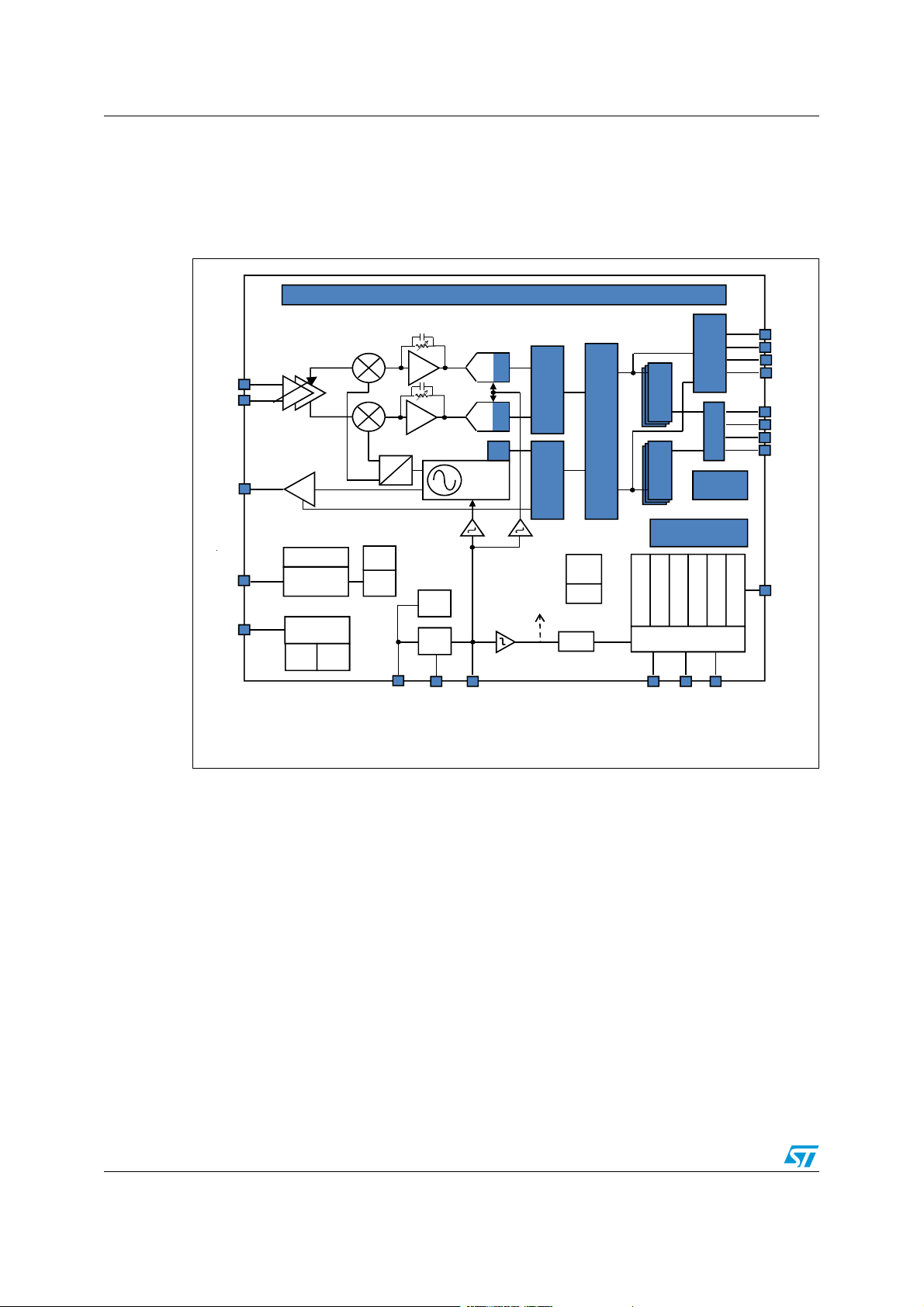
A simplified block diagram of the SPIRIT1 is shown in Figure 1.
Figure 1. SPIRIT1 block diagram
The receiver architecture is direct conversion. The received RF signal is amplified by a two-
stage low-noise amplifier (LNA) and down-converted in quadrature (I and Q) to the
intermediate frequency (IF). LNA and IF amplifiers make up the RX front-end (RXFE) and
have programmable gain. At IF, I/Q signals are digitized by ADCs. The demodulated data is
then provided to an external MCU either through the 96-byte RX FIFO, readable via SPI, or
directly using a programmable GPIO pin. A 128-bit AES co-processor is available to perform
(offline) data encryption/decryption to secure data transfer.
The transmitter part of the SPIRIT1 is based on direct synthesis of the RF frequency. The
power amplifier (PA) input is the LO generated by the RF synthesizer, while the output level
can be configured between -30 dBm and +11 dBm in 0.5 dB steps. The data to be
transmitted can be provided by an external MCU either through the 96-byte TX FIFO
writable via SPI, or directly using a programmable GPIO pin. The SPIRIT1 supports
frequency hopping, TX/RX and antenna diversity switch control, extending the link range
and improving performance.
The SPIRIT1 has a very efficient power management (PM) system.
8/91 Doc ID 022758 Rev 2

SPIRIT1 Introduction
An integrated switched mode power supply (SMPS) regulator allows operation from a
battery voltage ranging from +1.8 V to +3.6 V, and with power conversion efficiency of at
least 80%.
A crystal must be connected between XIN and XOUT. It is digitally configurable to operate
with different crystals. As an alternative, an external clock signal can be used to feed XIN for
proper operation. The SPIRIT1 also has an integrated low-power RC oscillator, generating
the 34.7 kHz signal used as a clock for the slowest timeouts (i.e. sleeping and backoff).
A standard 4-pin SPI bus is used to communicate with the external MCU. Four configurable
general purpose I/Os are available.
Doc ID 022758 Rev 2 9/91
Typical application diagram and pin description SPIRIT1
1.8V÷3.6V power supply
C0
C13
1 GPIO_0 SDN 15
SMPS Ext1 14
SMPS Ext2 13
TX 12
GND_PA 11
2 MISO
3 MOSI
4 SCLK
5 CSn
GPIO_1 20
GPIO_2 19
GPIO_3 18
VREG 17
VBAT 16
8 VBAT
6 XOUT
7 XIN
9 RFp
10 RFn
DIGITAL INTERFACE
SPIRIT1
DIE ATTACH PAD:
C9
C6
XTAL
C11
L7
Antenna
(50Ω )
L0
L1
L2
L3
C1
C2
C3
C5
L4
C4
L5
C10
L6
C7 C8
C0
L8
C12
C13
C15
C14
L9
AM09258V1
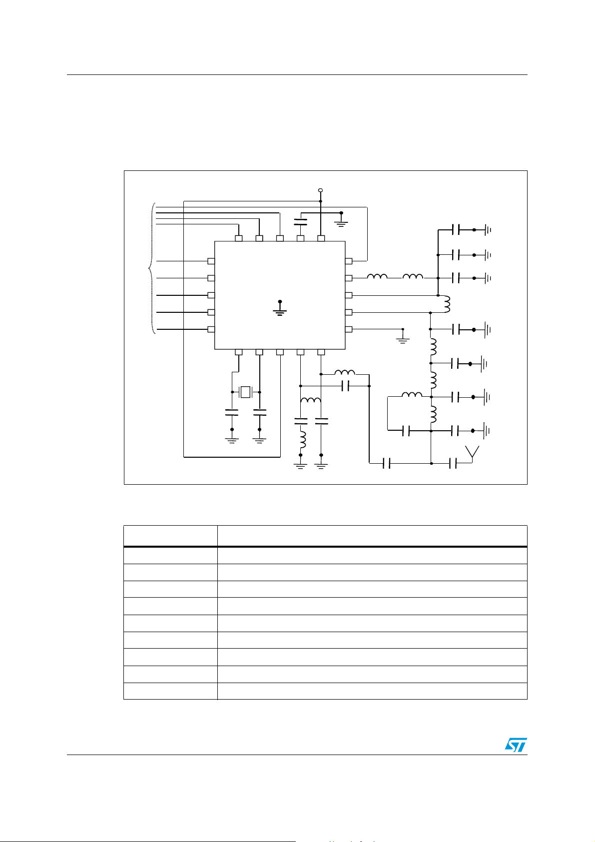
3 Typical application diagram and pin description
3.1 Typical application diagram
Figure 2. Suggested application diagram
Table 2. Description of the external components of the typical application
diagram
Components Description
C0 Decoupling capacitor for on-chip voltage regulator to digital part
C1, C2, C3, C14, C15 RF LC filter/matching capacitors
C4, C5 RF balun/matching capacitors
C6, C7, C8 RF balun/matching DC blocking capacitors
C9, C10 Crystal loading capacitors
C11, C12, C13 SMPS LC filter capacitor
L0 RF choke inductor
L1, L2, L3, L9 RF LC filter/matching inductors
L4, L5, L6 RF balun/matching inductors
10/91 Doc ID 022758 Rev 2

SPIRIT1 Typical application diagram and pin description
Table 2. Description of the external components of the typical application diagram
(continued)
Components Description
L7, L8 SMPS LC filter inductor
XTAL 24, 26, 48, 52 MHz
Ta bl e 2 assumes to cover all the frequency bands using only four sets of external
components.
Doc ID 022758 Rev 2 11/91

Pinout SPIRIT1
4 Pinout
Table 3. Pinout description
Pin Name I/O Description
1 GPIO_0 I/O See description of GPIOs below
2 MISO O SPI data output pin
3 MOSI I SPI data input pin
4 SCLK I SPI clock input pin
5 CSn I SPI chip select
6XOUTO
7XINI
8 VBAT VDD +1.8 V to +3.6 V input supply voltage
9RXpI
10 RXn I
11 GND_PA GND Ground for PA
12 TX O RF output signal
13 SMPS Ext2 I Regulated DC-DC voltage input
14 SMPS Ext1 O DC-DC output pin
15 SDN I
16 VBAT VDD +1.8 V to +3.6 V input supply voltage
17 VREG
18 GPIO3 I/O General purpose I/O that may be configured through the SPI
19 GPIO2 I/O
20 GPIO1 I/O
21 GND GND Exposed pad ground pin
(1)
VDD Regulated output voltage. A 100 nF decoupling capacitor is required
Crystal oscillator output. Connect to an external 26 MHz crystal or
leave floating if driving the XIN pin with an external signal source
Crystal oscillator input. Connect to an external 26 MHz crystal or to
an external source. If using an external clock source with no crystal,
DC coupling with a nominal 0.2 VDC level is recommended with
minimum AC amplitude of 400 mVpp
Differential RF input signal for the LNA. See application diagram for a
typical matching network
Shutdown input pin. 0-VDD V digital input. SDN should be = ‘0’ in all
modes except shutdown mode. When SDN =’1’ the SPIRIT1 is
completely shut down and the contents of the registers are lost
registers to perform various functions, including:
– MCU clock output
– FIFO status flags
– Wake-up input
– Battery level detector
– TX-RX external switch control
– Antenna diversity control
– Temperature sensor output
1. This pin is intended for use with the SPIRIT1 only. It cannot be used to provide supply voltage to other devices.
12/91 Doc ID 022758 Rev 2

SPIRIT1 Absolute maximum ratings and thermal data
5 Absolute maximum ratings and thermal data
Absolute maximum ratings are those values above which damage to the device may occur.
Functional operation under these conditions is not implied. All voltages are referred to GND.
Table 4. Absolute maximum ratings
Pin Parameter Value Unit
8,14,16 Supply voltage and SMPS output -0.3 to +3.6 V
17 DC voltage on VREG -0.3 to +1.4 V
1,3,4,5,15,18,19,20 DC voltage on digital input pins -0.3 to +3.6 V
2 DC voltage on digital output pins -0.3 to +3.6 V
11 DC voltage on analog pins -0.3 to +3.6 V
6,7,9,10 DC voltage on RX/XTAL pins -0.3 to +1.4 V
13 DC voltage on SMPS Ext2 pin -0.3 to +1.4 V
12 DC voltage on TX pin -0.3 to +3.6 V
T
STG
V
ESD-HBM
Storage temperature range -40 to +125 °C
Electrostatic discharge voltage ±1.0 KV
Table 5. Thermal data
Symbol Parameter QFN20 Unit
R
thj-amb
Thermal resistance junction-ambient 45 °C/W
Table 6. Recommended operating conditions
Symbol Parameter Min. Typ. Max. Unit
V
BAT
T
Operating battery supply voltage 1.8 3 3.6 V
Operating ambient temperature range -40 85 °C
A
Doc ID 022758 Rev 2 13/91
Characteristics SPIRIT1
6 Characteristics
6.1 General characteristics
Table 7. General characteristics
Symbol Parameter Min. Typ. Max. Unit
FREQ Frequency range
Air data rate for each modulation scheme
Optional Manchester and 3 out of 6 encoding/decoding can be selected
2-FSK 1
DR
GMSK (BT=1, BT=0.5) 1 500 kBaud
GFSK (BT=1, BT=0.5) 1 500 kBaud
MSK 1 500 kBaud
OOK/ASK 1 250 kBaud
6.2 Electrical specifications
6.2.1 Electrical characteristics
Characteristics measured over recommended operating conditions unless otherwise
specified. Typical values are referred to T
to a 50 Ohm antenna connector, via the reference design.
= 25 °C, V
A
150
300 348 MHz
387 470 MHz
779 956 MHz
= 3.0 V. All performance is referred
BAT
174 MHz
-
500 kBaud
-
14/91 Doc ID 022758 Rev 2

SPIRIT1 Characteristics
Table 8. Power consumption
Symbol Parameter Test conditions Min. Typ. Max. Unit
RX
(1)
(1)
(1)
(1)
(1)
(1)
2.5
650 nA
950 nA
400 µA
4.5 mA
9mA
21
22
19.5
21
6
6.5
7
7
nA
-
mA
I
BAT
1. See Table 17.
Supply current
Shutdown
Standby
Sleep
Ready (default mode)
Tu ni n g
(1)
TX
+11 dBm 169 MHz
(1)
TX
+11 dBm 315 MHz
(1)
TX
+11 dBm 433 MHz
(1)
TX
+11 dBm 868 MHz
(1)
TX
-8 dBm 169 MHz
(1)
TX
-8 dBm 315 MHz
(1)
TX
-7 dBm 433 MHz
(1)
TX
-7 dBm 868 MHz
6.2.2 Digital SPI
Table 9. Digital SPI input and output (SDO, SDI, SCLK, CSn, and SDN) and GPIO
Symbol Parameter Test condition Min. Typ. Max. Unit
Clock frequency 10 MHz
clk
Port I/O capacitance 1.4 pF
IN
Rise time
Fall time
Logic high level input
IH
voltage
T
T
f
C
RISE
FAL L
V
specification (GPIO_1-4)
0.1*VDD to 0.9*VDD,
CL=20 pF (low output
current programming)
0.1*VDD to 0.9*VDD,
CL=20 pF (high output
current programming)
0.1*VDD to 0.9*VDD,
CL=20 pF (low output
current programming)
0.1*VDD to 0.9*VDD,
CL=20 pF (high output
current programming)
VDD/2
+0.3
3.5
ns
2
5.5
ns
2.8
V
V
Logic low level input
IL
voltage
VDD/8
+0.3
V
Doc ID 022758 Rev 2 15/91

Characteristics SPIRIT1
Table 9. Digital SPI input and output (SDO, SDI, SCLK, CSn, and SDN) and GPIO
specification (GPIO_1-4) (continued)
Symbol Parameter Test condition Min. Typ. Max. Unit
IOH = -2.4 mA (-4.2 mA if
V
V
High level output voltage
OH
Low level output voltage
OL
high output current
capability is
programmed).
IOL = +2.4 mA (+4 mA if
high output current
capability is
programmed).
(5/8)*
VDD+
0.1
0.5 V
6.2.3 RF receiver
Characteristics measured over recommended operating conditions unless otherwise
specified. All typical values are referred to T
= 25 °C, V
A
the RX signal. All performance is referred to a 50 Ohm antenna connector, via the reference
design.
Table 10. RF receiver characteristics
Symbol Parameter Test condition Min. Typ. Max. Unit
169.4-169.475 MHz, 433-435
RL Return loss
CH
BW
Receiver channel bandwidth 6 800 kHz
MHz, 868-868.6 MHz, 310-320
MHz, 902-928 MHz
169MHz 2-FSK 1.2Kbps
(4 kHz dev. CH Filter=10kHz)
(1)
= 3.0 V, no frequency offset in
BAT
-10 dB
-117 dBm
V
169MHz GFSK (BT=0.5)
Sensitivity, 1% BER (according
to W-MBUS N mode
specification)
RX
SENS
Sensitivity, 1% PER (packet
length = 20 bytes) FEC
DISABLED
16/91 Doc ID 022758 Rev 2
2.4Kbps (2.4 kHz dev. CH
Filter=7kHz)
169MHz 2-FSK 38.4Kbps (50
kHz dev. CH Filter=100 kHz)
169MHz GFSK (BT=0.5)
50Kbps (25 kHz dev. CH
Filter=100 kHz)
315 MHz 2-FSK 1.2 kbps (5.2
kHz dev. CH BW=58 kHz)
315 MHz MSK 500 kbps (RX
filter BW=812 kHz)
-115 dBm
-104 dBm
-104 dBm
-109 dBm
-88 dBm

SPIRIT1 Characteristics
Table 10. RF receiver characteristics (continued)
Symbol Parameter Test condition Min. Typ. Max. Unit
RX
SENS
Sensitivity, 1% PER (packet
length = 20 bytes) FEC
DISABLED
Sensitivity, 1% PER (packet
length = 20 bytes) FEC
DISABLED
433 MHz 2-FSK 1.2 kbps (1
kHz dev. CH BW=6 kHz)
433 MHz GFSK 1.2 kbps BT=1
(5.2 kHz dev. CH BW=58 kHz)
433 MHz GFSK 38.4 kbps
BT=1 (20 kHz dev. CH
BW=100 kHz)
433 MHz GFSK 250 kbps
BT=1 (127 kHz dev. CH
BW=540 kHz)
868 MHz 2-FSK 1.2 kbps (1
kHz dev. CH BW=6 kHz)
868 MHz GFSK 1.2 kbps BT=1
(5.2 kHz dev. CH BW=58 kHz)
868 MHz GFSK 38.4 kbps
BT=1 (20 kHz dev. CH
BW=100 kHz)
868 MHz GFSK 250 kbps
BT=1 (127 kHz dev. CH
BW=540 kHz)
868 MHz MSK 250 kbps (CH
BW=540 kHz)
-117 dBm
-103 dBm
-103 dBm
-92 dBm
-118 dBm
-109 dBm
-106 dBm
-97 dBm
-95 dBm
Sensitivity, 1% PER (packet
915 MHz 2-FSK 1.2 kbps (5.2
kHz dev. CH BW=58 kHz)
915 MHz 2-FSK 38.4 kbps (20
kHz dev. CH BW=100 kHz)
-107 dBm
-105 dBm
length = 20 bytes) FEC
DISABLED
915 MHz 2-FSK 250 kbps (127
kHz dev. CH BW=540 kHz)
915 MHz MSK 500 kbps (RX
filter BW=812 kHz)
-98 dBm
-96 dBm
433 MHz OOK 1.2 kbps -116 dBm
Sensitivity, 1% PER (packet
length = 20 bytes) FEC
DISABLED
(2)
433 MHz OOK 2.4 kbps -113 dBm
433 MHz OOK 38.4 kbps -99 dBm
433 MHz OOK 250 kbps -87 dBm
868 MHz OOK 1.2 kbps -116 dBm
Sensitivity, 1% PER (packet
length = 20 bytes) FEC
DISABLED
(2)
868 MHz OOK 2.4 kbps -113 dBm
868 MHz OOK 38.4 kbps -100 dBm
868 MHz OOK 250 kbps -90 dBm
Saturation 1% PER (packet
P
SAT
length = 20 bytes) FEC
868 MHz GFSK 38.4 kbps -5 dBm
DISABLED
Doc ID 022758 Rev 2 17/91

Characteristics SPIRIT1
Table 10. RF receiver characteristics (continued)
Symbol Parameter Test condition Min. Typ. Max. Unit
IIP3 Input third order intercept Input power -50 dBm 915 MHz -31 dBm
Desired channel 3 dB above
C/I
1-CH
Adjacent channel rejection,
1% PER (packet length = 20
(3)
bytes) FEC DISABLED 868
MHz
sensitivity level. 12.5 kHz
channel spacing, 2-FSK 1.2
kbps, (RX filter BW=6 kHz)
Desired channel 3 dB above
sensitivity level. 100 kHz
channel spacing, 2-FSK 1.2
kbps, (RX filter BW=58 kHz)
Desired channel 3 dB above
sensitivity level. 200 kHz
channel spacing, GFSK 38
kbps
Desired channel 3 dB above
sensitivity level. 750 kHz
channel spacing, MSK 250
kbps
Desired channel 3 dB above
sensitivity level. 12.5 kHz
channel spacing, 2-FSK 1.2
kbps, (RX filter BW=6 kHz)
55 dB
47 dB
36 dB
41 dB
57 dB
C/I
IM
RX
2-CH
REJ
BLK
Alternate channel rejection,
1% PER (packet length = 20
(3)
bytes)
FEC DISABLED
868 MHz
Image rejection, 1% PER
(packet length = 20 bytes) 1%
(3)
PER (packet length = 20 bytes)
FEC DISABLED
Blocking at offset above the
(4)
upper band edge and below the
lower band edge 1% BER
Desired channel 3 dB above
sensitivity level. 100 kHz
channel spacing, 2-FSK 1.2
kbps, (RX filter BW=58 kHz)
Desired channel 3 dB above
sensitivity level. 200 kHz
channel spacing, GFSK 38
kbps
Desired channel 3 dB above
sensitivity level. 750 kHz
channel spacing, MSK 250
kbps
868 MHz GFSK 38.4 kbps
BT=1 (20kHz dev. CH BW=100
kHz), desired channel 3 dB
above the sensitivity limit, with
IQC correction.
@ 2 MHz offset, 868 MHz
GFSK 38.4kbps, desired
channel 3 dB above the
sensitivity limit
@ 10 MHz offset, 868 MHz
GFSK 38.4kbps, desired
channel 3 dB above the
sensitivity limit.
47 dB
41 dB
56 dB
48 dB
-42 dBm
-40 dBm
18/91 Doc ID 022758 Rev 2

SPIRIT1 Characteristics
Table 10. RF receiver characteristics (continued)
Symbol Parameter Test condition Min. Typ. Max. Unit
Below 1 GHz -58 dBm
RX
SPUR
Spurious emissions (maximum
values according to ETSI EN
300 220-1)
Above 1 GHz up to 4 GHz for
frequency band < 470 MHz, up
to 6 GHz for frequency band >
-61 dBm
470 MHz
1. Guaranteed in an entire single sub band. Reference design can be different for different application bands.
2. In OOK modulation, indicated value represents mean power.
3. Interferer is CW signal (as specified by ETSI EN 300 220 v1).
4. Blocker is CW signal (as specified by ETSI EN 300 220 v1)
6.2.4 RF transmitter
Characteristics measured over recommended operating conditions unless otherwise
specified. All typical values are referred to T
referred to a 50 Ohm antenna connector, via the reference design.
Table 11. RF transmitter characteristics
= 25 °C, V
A
= 3.0 V. All performance is
BAT
Symbol Parameter Test conditions Min. Typ. Max. Unit
Delivered to a 50 Ohm single-
ended load via reference
design
11 dBm
P
MAX
Maximum output
power
(1)
Delivered to a 50 Ohm single-
P
MIN
Minimum output power
ended load via reference
-36 dBm
design
P
STEP
Output power step 0.5 dB
Doc ID 022758 Rev 2 19/91

Characteristics SPIRIT1
Table 11. RF transmitter characteristics (continued)
Symbol Parameter Test conditions Min. Typ. Max. Unit
P
SPUR,ETSI
Unwanted emissions
according to ETSI
EN300 220-1(harmonic
included, using
reference design)
RF = 170 MHz, frequencies
below 1 GHz
RF = 170 MHz, Frequencies
above 1 GHz
RF = 170 MHz, frequencies
within 47-74, 87.5-108,174-
230,470-862 MHz
RF = 434 MHz, frequencies
below 1 GHz
RF = 434 MHz, Frequencies
above 1 GHz
RF = 434 MHz, frequencies
within 47-74, 87.5-108,174-
230,470-862 MHz
RF = 868 MHz, frequencies
below 1 GHz
RF = 868 MHz, Frequencies
above 1 GHz
RF = 868 MHz, frequencies
within 47-74, 87.5-108,174-
230,470-862 MHz
-36 dBm
< -60 dBm
-55 dBm
-42 dBm
-46 dBm
-61 dBm
-51 dBm
-40 dBm
-54 dBm
20/91 Doc ID 022758 Rev 2

SPIRIT1 Characteristics
Table 11. RF transmitter characteristics (continued)
Symbol Parameter Test conditions Min. Typ. Max. Unit
RF = 310-320 MHz,
harmonics (measured with
max output power)
-37 dBm
P
SPUR,FCC
Unwanted emissions
according to FCC part
15(harmonic included,
using reference design)
RF = 310-320 MHz, 1.705
MHz <f< 30 MHz
RF = 310-320 MHz, 30 MHz
<f< 88 MHz
RF = 310-320 MHz, 88 MHz
<f< 216 MHz
RF = 310-320 MHz, 216 MHz
<f< 960 MHz
RF = 310-320 MHz, 960 MHz
<f
RF = 902-928 MHz, 1.705
MHz <f< 30 MHz (@ max
output power)
RF = 902-928 MHz, 30 MHz
<f< 88 MHz (@ max output
power)
RF = 902-928 MHz, 88 MHz
<f< 216 MHz (@ max output
power)
RF = 902-928 MHz, 216 MHz
<f< 960 MHz (@ max output
power)
<-60 dBm
<-60 dBm
<-60 dBm
<-60 dBm
<-60 dBm
<-70 dBm
<-70 dBm
<-70 dBm
-52 dBm
RF = 902-928 MHz, 960 MHz
<f (@ max output power)
nd
and 7th harmonics -25 dBc
2
-41 dBm
Doc ID 022758 Rev 2 21/91

Characteristics SPIRIT1
Table 11. RF transmitter characteristics (continued)
Symbol Parameter Test conditions Min. Typ. Max. Unit
RF = 312-315 MHz, frequency
below 1 GHz (@ max output
power, according to ARIB
STD-T93)
RF = 312-315 MHz, frequency
above 1 GHz (@ max output
power, according to ARIB
STD-T93)
RF = 426-470 MHz (@ max
output power, according to
ARIB STD-T67)
RF = 920-924 MHz, f< 710
MHz (@ max output power,
according to ARIB STD-T108)
RF = 920-924 MHz, 710 MHz
<f< 915 MHz (@ max output
power, according to ARIB
STD-T108)
-41 dBm
-48 dBm
<-40 dBm
<-55 dBm
-55 dBm
P
SPUR,ARIB
Unwanted emissions
according to ARIB
RF = 920-924 MHz, 915 MHz
<f< 920 MHz (@ max output
power, according to ARIB
STD-T108)
RF = 920-924 MHz, 920 MHz
<f< 924 MHz (@ max output
power, according to ARIB
STD-T108)
RF = 920-924 MHz, 924 MHz
<f< 930 MHz (@ max output
power, according to ARIB
STD-T108)
RF = 920-924 MHz, 930 MHz
<f< 1000 MHz (@ max output
power, according to ARIB
STD-T108)
RF = 920-924 MHz, 1000
MHz <f< 1215 MHz (@ max
output power, according to
ARIB STD-T108)
RF = 920-924 MHz, 1215
MHz <f (@ max output power,
according to ARIB STD-T108)
-46 dBm
<-60 dBm
-47 dBm
-55 dBm
<-60 dBm
-38 dBm
22/91 Doc ID 022758 Rev 2

SPIRIT1 Characteristics
Table 11. RF transmitter characteristics (continued)
Symbol Parameter Test conditions Min. Typ. Max. Unit
170 MHz, using reference
design
315 MHz, using reference
design
433 MHz, using reference
PA
LOAD
Optimum load
impedance (simulated
v a l u e s )
868 MHz, using reference
design
design
915 MHz, using reference
design
922 MHz, using reference
design
1. In ASK/OOK modulation, indicated value represents peak power.
46 + j36 Ohm
25 + j27 Ohm
29 + j19 Ohm
34 - j7 Ohm
15 + j28 Ohm
42 - j15 Ohm
6.2.5 Crystal oscillator
Characteristics measured over recommended operating conditions unless otherwise
specified. All typical values are referred to T
= 25 °C, V
A
characteristics are referred to 915 MHz band.
Table 12. Crystal oscillator characteristics
Symbol Parameter Test conditions Min. Typ. Max. Unit
= 3.0 V. Frequency synthesizer
BAT
XTAL
F
TOL
Crystal frequency 26 MHz
F
Frequency tolerance
(1)
± 40 ppm
100 Hz -90 dBc/Hz
PN
XTAL
Minimum requirement on
external reference phase noise
mask (Fxo=26 MHz), to avoid
degradation on synthesizer
phase/noise
1 kHz -120 dBc/Hz
10 kHz -135 dBc/Hz
100 kHz -140 dBc/Hz
1 MHz -140 dBc/Hz
T
START
1. Including initial tolerance, crystal loading, aging, and temperature dependence. The acceptable crystal tolerance depends
on RF frequency and channel spacing/bandwidth.
2. Startup times are crystal dependent. The crystal oscillator transconductance can be tuned to compensate the variation of
crystal oscillator series resistance.
Startup time
(2)
V
=1.8 V 100 280 300 µs
BAT
Doc ID 022758 Rev 2 23/91

Characteristics SPIRIT1
Table 13. Ultra low power RC oscillator
Symbol Parameter Test conditions Min. Typ. Max. Unit
Calibrated RC oscillator
RC
Calibrated frequency
F
frequency is derived from
crystal oscillator frequency.
Digital clock domain 26 MHz
34.7 kHz
-
RC
TOL
Frequency accuracy after
calibration
±1 %
Table 14. N-Fractional ΣΔ frequency synthesizer characteristics
Symbol Parameter Test conditions Min. Typ. Max. Unit
F
RES
Frequency resolution - 100 Hz
10 kHz -100 -97 -94 dBc/Hz
100 kHz -104 -101 -99 dBc/Hz
PN
SYNTH
RF carrier phase noise
(915 MHz band)
200 kHz -105 -102 -100 dBc/Hz
500 kHz -112 -110 -107 dBc/Hz
1 MHz -120 -118 -116 dBc/Hz
2 MHz -123 -121 -119 dBc/Hz
TO
SET
CAL
TIME
PLL turn-on/hop time 60 80 µs
PLL RX/TX settling time
TIME
PLL calibration time 54 µs
TIME
Settling time from RX to TX
and from TX to RX
8.5 µs
6.2.6 Sensors
Characteristics measured over recommended operating conditions unless otherwise
specified. All typical values are referred to T
Table 15. Analog temperature sensor characteristics
= 25 °C, V
A
(1)
Symbol Parameter Test conditions Min. Typ. Max. Unit
T
T
SLOPE
V
TS-OUT
Error in temperature Across all the temperature range ±2.5 °C
ERR
Temperature coefficient 2.5
Output voltage level 0.92 V
Buffered output (low output
impedance, about 400 Ohm)
T
Current consumption
ICC
Not buffered output (high output
impedance, about 100 kΩ)
1. The temperature readout is a trigger based function. Some processing time is allowed. So, start of conversion trigger ->
end of conversion status + read out register.
24/91 Doc ID 022758 Rev 2
BAT
= 3.0 V.
600 µA
10 µA
mV/
°C

SPIRIT1 Characteristics
Table 16. Battery indicator and low battery detector
(1)
Symbol Parameter Test conditions Min. Typ. Max. Unit
V
Battery level thresholds 2.1 2.7 V
BLT
Measured in slow battery
variation (static) conditions
1.535 V
(inaccurate)
V
Brownout threshold
BOT
Measured in slow battery
variation (static) conditions
1.684 V
(accurate)
BOT
1. For battery powered equipment, the TX does not transmit at a wrong frequency under low battery voltage conditions. It
either remains on channel or stops transmitting. The latter can of course be realized by using a lock detect and/or by
switching off the PA under control of the battery monitor. For testing reasons this control is enabled/disabled by SPI.
Brownout threshold hysteresis 70 mV
hyst
Doc ID 022758 Rev 2 25/91
Operating modes SPIRIT1
2%!$9
34!.$"9
3,%%0
2848,/#+
3(54$/7.
!-6
7 Operating modes
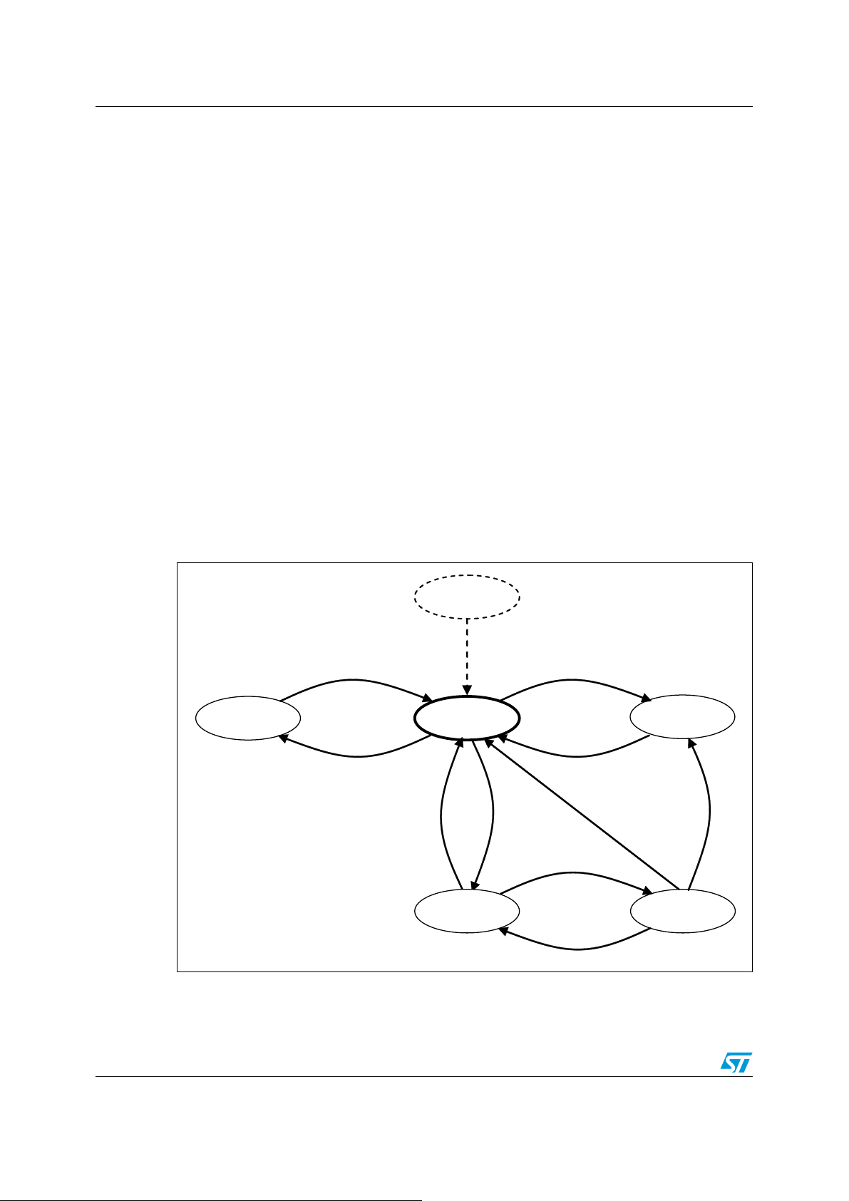
The SPIRIT1 is provided with a built-in main controller which controls the switching between
the two main operating modes: transmit (TX) and receive (RX).
In shutdown condition (the SPIRIT1 can be switched on/off with the external pin SDN, all
other functions/registers/commands are available through the SPI interface and GPIOs), no
internal supply is generated (in order to have minimum battery leakage), and hence, all
stored data and configurations are lost. From shutdown, the SPIRIT1 can be switched on
from the SDN pin and goes into READY state, which is the default, where the reference
signal from XO is available.
From READY state, the SPIRIT1 can be moved to LOCK state to generate the high
precision LO signal and/or TX or RX modes. Switching from RX to TX and vice versa can
happen only by passing through the LOCK state. This operation is normally managed by
radio control with a single user command (TX or RX). At the end of the operations above,
the SPIRIT1 can return to its default state (READY) and can then be put into a sleeping
condition (SLEEP state), having very low power consumption. If no timeout is required, the
SPIRIT1 can be moved from READY to STANDBY state, which has the lowest possible
current consumption while retaining FIFO, status and configuration registers. To manage the
transitions towards and between these operating modes, the controller works as a statemachine, whose state switching is driven by SPI commands. See Figure 3 for state diagram
and transition time between states.
Figure 3. Diagram and transition
The SPIRIT1 radio control has three stable states (READY, STANDBY, LOCK) which may be
defined stable, and they are accessed by the specific commands (respectively READY,
26/91 Doc ID 022758 Rev 2

SPIRIT1 Operating modes
STANDBY, and LOCKRX/LOCKTX), which can be left only if any other command is used. All
other states are transient, which means that, in a typical configuration, the controller
remains in those states, at most for any timeout timer duration. Also the READY and LOCK
states behave as transients when they are not directly accessed with the specific commands
(for example, when LOCK is temporarily used before reaching the TX or RX states).
Table 17. States
State/mode Digital LDO SPI Xtal RF Synth.
SHUTDOWN
STANDBY
SLEEP On Off Off On 350 µs 350 µs
READY (Default) On On Off Don’t care 110 µs 110 µs
LOCK On On On Don’t care NA NA
RX On On On Don’t care 20 µs NA
TX On On On Don’t care NA 20 µs
OFF (register
contents lost)
ON (FIFO and
register
contents
retained)
Off Off Off Off NA NA
On Off Off Off 320 µs 320 µs
Wake-up
timer
Response time to
TX RX
Note: Response time SHUTDOWN to READY is ~1 ms.
READY state is the default state after the power-on reset event. In the steady condition, the
XO is settled and usable as the time reference for RCO calibration, for frequency synthesis,
and as the system clock for the digital circuits.
The TX and RX modes can be activated directly by the MCU using the TX and RX
commands, or automatically if the state machine wakes up from SLEEP mode and some
previous TX or RX is pending.
(a)
In LOCK state the synthesizer is in a locking condition
. If LOCK state is reached using
either one of the two specific commands (LOCKTX or LOCKRX), the state machine remains
in LOCK state and waits for the next command. This feature can be used by the MCU to
perform preliminary calibrations, as the MCU can read the calibration word in the
RCO_VCO_CALIBR_OUT register and store it in a non-volatile memory, and after that it
requires a further tuning cycle.
When TX is activated by the TX command, the state machine goes into TX state and
remains there until the current packet is fully transmitted or, in the case of direct mode TX,
TXFIFO underflow condition is reached or the SABORT command is applied.
a. LOCK state is reached when one of the following events occurs first: lock detector assertion or locking timeout
expiration.
Doc ID 022758 Rev 2 27/91

Operating modes SPIRIT1
After TX completion, the possible destinations are:
● TX, if the persistent-TX option is enabled in the PROTOCOL configuration registers
● PROTOCOL, if some protocol option (e.g. automatic re-transmission) is enabled
● READY, if TX is completed and no protocol option is in progress.
Similarly, when RX is activated by the RX command, the state machine goes into RX state
and remains there until the packet is successfully received or the RX timeout expires. In
case of direct mode RX, the RX stops when the RXFIFO overflow condition is reached or
the SABORT command is applied. After RX completion, the possible destinations are:
● RX, if the persistent-RX option is enabled in the PROTOCOL configuration registers
● PROTOCOL, if some protocol option (e.g. automatic acknowledgement) is enabled
● READY, if RX is completed and the LDCR mode is not active
● SLEEP, if RX is completed and the LDCR mode is active.
The SABORT command can always be used in TX or RX state to break any deadlock
condition and the subsequent destination depends on SPIRIT1 programming according to
the description above.
Commands are used in the SPIRIT1 to change the operating mode, to enable/disable
functions, and so on. A command is sent on the SPI interface and may be followed by any
other SPI access without pulling CSn high.
The complete list of commands is reported in Ta bl e 18 . Note that the command code is the
second byte to be sent on the MOSI pin (the first byte must be 0x80).
Table 18. Commands list
Command
code
0x60 TX READY Start to transmit
0x61 RX READY Start to receive
0x62 READY
0x63 STANDBY READY Go to STANDBY
0x64 SLEEP READY Go to SLEEP
0x65 LOCKRX READY
0x66 LOCKTX READY
0x67 SABORT TX, RX Exit from TX or RX states and go to READY state
0x68 LDC_RELOAD All
0x69
Command name Execution state Description
SEQUENCE_UPDA
TE
STANDBY, SLEEP,
LOCK
All
Go to READY
Go to LOCK state by using the RX configuration of the
synthesizer
Go to LOCK state by using the TX configuration of the
synthesizer
Reload the LDC timer with the value stored in the
LDC_PRESCALER/COUNTER registers
Reload the packet sequence counter with the value
stored in the PROTOCOL[2] register.
0x6A AES Enc All Start the encryption routine
0x6B AES Key All Start the procedure to compute the key for decryption
0x6C AES Dec All Start decryption using the current key
28/91 Doc ID 022758 Rev 2

SPIRIT1 Operating modes
!-6
Table 18. Commands list (continued)
Command
code
0x6D AES KeyDec All Compute the key and start decryption
0x70 SRES All Reset
0x71 FLUSHRXFIFO All Clean the RX FIFO
0x72 FLUSHTXFIFO All Clean the TX FIFO
Command name Execution state Description
The commands are immediately valid after SPI transfer completion (i.e. no need for any CSn
positive edge).
7.1 Reset sequence
SPIRIT1 is provided with an automatic power-on reset (POR) circuit which generates an
internal RESETN active (low) level for a time T
release threshold voltage V
(provided that SDN is low), as shown below. The same reset
RRT
pulse is generated after a step-down on the input pin SDN (provided that VDD>V
Figure 4. Power-on reset timing and limits
after the VDD reaches the reset
RESET
6$$NOMINAL
RRT
).
6
2%3%4.
3
6$$
T
The parameters V
RRT
and T
4
are fixed by design. At RESET, all the registers are
RESET
initialized to their default values. Typical and extreme values are reported in the following
table.
Doc ID 022758 Rev 2 29/91

Operating modes SPIRIT1
Table 1 9. POR param e ters
Symbol Parameter Comment Min. Typ. Max. Unit
V
T
RESET
RRT
Reset startup threshold
voltage
Reset pulse width 0.5 1.0 1.5 ms
0.5 V
Note: An SRES command is also available which generates an internal RESET of the SPIRIT1.
7.2 Timer usage
Most of the timers are programmable via R/W registers. All timer registers are made up of
two bytes: the first byte is a multiplier factor (prescaler); the second byte is a counter value.
MSB LSB
15 PRESCALER 8 7 COUNTER 0
Timer period= PRESCALER x CONTER x Tclk
For example, using a 26 MHz crystal oscillator (Tclk = 38 ns) and a PRESCALER of 27
(decimal), the COUNTER time base is about 1 µs.
Note: If the counter register value (prescaler register value) is 0, the related timer never stops
(infinite timeout), despite the value written in the prescaler register (counter register).
The available timers and their features are listed in the following table.
Table 20. SPIRIT1 timers description and duration
No. Register name Description Source
1 RX_TIMEOUT_PRESCALER RX operation timeout XTAL ~46μs ~3s
2 RX_TIMEOUT_COUNTER
3 LDCR_PRESCALER Wake-up period RCO ~29μs ~2s
4 LDCR_COUNTER
Time
step
Max. time
Note: For LDCR_COUNTER and LDCR_PRESCALER only, the effective number of cycles
counted is given by the value + 1 (e.g. counter=1 and prescaler=1 produces 2 x 2=4 counts,
counter=1 and prescaler=2 produces 2 x 3=6 counts, etc.).
7.3 Low duty cycle reception mode
The SPIRIT1 provides an operating mode, low duty cycle reception (LDCR), which is an
operating mode that allows operation with very low power consumption, while at the same
time keeping an efficient communication link. The LDCR mode is enabled by setting the
LDCR_MODE bit in the PROTOCOL registers.
30/91 Doc ID 022758 Rev 2

SPIRIT1 Operating modes
!#4)6% 3,%%0).' )$,%
475
4
)$,%
7AKE 5P
)NTERRUPT
39.#RECEIVED
)NTERRUPT
!-6
This mode is available for both the transmitter and receiver and it is designed to allow for at
most one sequence RX+TX or TX+RX.
The device provides a set of timers to efficiently handle low duty cycle reception (LDCR).
When LDCR is enabled the device runs on the 34.7 kHz RC oscillator keeping unused
blocks off.
LDCR is controlled essentially by the wake-up period (T
), which periodically wakes up
WU
the SPIRIT1 to perform a transmission or a reception.
In reception mode, it is also relevant to set up the RX timeout in order to minimize the
amount of time the SPIRIT1 waits for a packet during T
When setting T
, care should be taken when considering the analog settling time which is
WU
required before the radio becomes fully operative for transmission or reception (T
WU
.
in
IDLE
Figure 5).
Figure 5. LDCR mode timing
The T
this causes power waste. In order to minimize T
time can be longer than the minimum required to get analog circuits settling, and
IDLE
, the SPIRIT1 supports the runtime
IDLE
phasing of the internal wake-up timer, as follows:
● The value of the wake-up timer can be reloaded during runtime using the
LDCR_RELOAD command with the values written in the
LDCR_RELOAD_PRESCALER/COUNTER registers. In doing so, the counting can be
delayed or anticipated
● Alternatively, the wake-up timer can be automatically reloaded at the time the SYNC is
received. This option must be enabled on the PROTOCOL register and it is available
only for LDC mode in reception.
7.4 CSMA/CA engine
The CSMA/CA engine is a channel access mechanism based on the rule of sensing the
channel before transmitting. This avoids the simultaneous use of the channel by different
transmitters and increases the probability of correct reception of data being transmitted.
CSMA is an optional feature that can be enabled on the basis of user needs.
When CSMA is enabled, the device performs a clear channel assessment (CCA) before
transmitting any data. In SPIRIT1 implementation, CCA is based on a comparison of the
channel RSSI with a programmable static carrier sense threshold.
If the CCA finds the channel busy, a backoff procedure may be activated to repeat the CCA
process a certain number of times, until the channel is found to be idle. Each time that CCA
is retried, a counter (NB) is incremented by one, up to the upper limit (NB
).
max
Doc ID 022758 Rev 2 31/91

Operating modes SPIRIT1
When the limit is reached, an NBACKOFF_MAX interrupt request is raised towards the
MCU, to notify that the channel has been repeatedly found busy and so the transmission
has not been performed.
While in backoff, the device stays in SLEEP/READY state in order to reduce power
consumption.
CCA may optionally be persistent, i.e., rather than entering backoff when the channel is
found busy, CCA continues until the channel becomes idle or until the MCU stops it.
The thinking behind using this option is to give the MCU the possibility of managing the CCA
by itself, for instance, with the allocation of a transmission timer: this timer would start when
MCU finishes sending out data to be transmitted, and would end when MCU expects that its
transmission takes place, which would occur after a period of CCA.
The choice of making CCA persistent should come from trading off transmission latency,
under the direct control of the MCU, and power consumption, which would be greater due to
a busy wait in reception mode.
The overall CSMA/CA flowchart is shown in Figure 6, where T
cca
and T
are two of the
listen
parameters controlling the clear channel assessment procedure. Design practice
recommends that these parameters average the channel energy over a certain period
expressed as a multiple of the bit period (T
covering longer periods (T
). The measurement is performed directly by checking the
listen
) and repeat such measurement several times
cca
carrier sense (CS) generated by the receiver module.
32/91 Doc ID 022758 Rev 2

30)COMMAND
48
."
3EEDRELOAD
#3-!?/.
3$.
3(54$/7.
2%!$9
3$.INTERNAL0/2
3ETTLING
ON2ESET
48SETTLING
48MODE
TRANSMITAPACKET
PERSISTENT
#3-!?0%23?/.
28MODE
CHANNELBUSY
#3
#3TIMEOUT
4
LISTEN
EXPIRATION
.O
9ES
9ES
2ESTART#ARRIER
3ENSETIMERS
9ES
NUMBEROFRETRIES
."."
MAX
3,%%0
.O
(AS"/WAIT
ELAPSED
"/RAND
."
§"5
."."
#3- !MODE
ENABLED
9ES
#3PERIOD
.O
4
CCA
EXPIRATION
.O
9ES
.O
9ES
.O
.O
9ES
#3-!
#3-!
2%!$9
!-6
SPIRIT1 Operating modes
Figure 6. CSMA flowchart
To avoid any wait synchronization between different channel contenders, which may cause
successive failing CCA operations, the backoff wait time is calculated randomly between 0
and a contention window. The backoff time BO is expressed as a multiple of backoff time
units (BU). The contention window is calculated on the basis of the binary exponential
Doc ID 022758 Rev 2 33/91

Operating modes SPIRIT1
backoff (BEB) technique, which doubles the size of the window at each backoff retry (stored
in the NB counter):
BO= rand(0,2
NB
)×BU
The CSMA procedure is then controlled by the following parameters:
SEED_RELOAD: enables/disables the reload of the seed used by the backoff random
generator at the start of each CSMA procedure (at the time when the counter is reset, i.e.
NB=0). If this functionality is not enabled, the seed is automatically generated and updated
by the generator circuit itself.
CSMA_ON: enables/disables the CSMA procedure (11
th
bit of the PROTOCOL[1] register);
this bit is checked at each packet transmission.
CSMA_PERS_ON: makes the carrier sense persistent, i.e. the channel is continuously
th
monitored until it becomes free again, skipping the backoff waiting steps (9
bit of the
PROTOCOL[1] register); the MCU can stop the procedure with an SABORT command.
BU_COUNTER_SEED_MSByte/LSByte: these bytes are used to set the seed of the
pseudo-random number generator when the CSMA cycle starts (CSMA_CONFIG[3:2]
registers), provided that the SEED_RELOAD bit is enabled. Value 0 is not allowed, because
the pseudo-random generator does not work in that case.
(b)
BU_PRESCALER[5:0]: prescaler which is used to configure the backoff time unit
BU=BU_PRESCALER in Figure 6 (field of the CSMA_CONFIG[1] register).
CCA_PERIOD[1:0]: code which programs the T
time (expressed as a multiple of Tbit
cca
samples) between two successive CS samplings (field of the CSMA_CONFIG[1] register),
as follows:
● 00 64×Tbit
● 01 128×Tbit
● 10 256×Tbit
● 11 512×Tbit.
CCA_LENGTH[3:0]: configuration of T
= [1..15] x T
listen
cca
NBACKOFF_MAX[2:0]: max. number of backoff cycles.
b. Note that the backoff timer is clocked on the 34.7 kHz clock, because, in this case, the SPIRIT1 is in SLEEP
state, in order to reduce power consumption.
34/91 Doc ID 022758 Rev 2

SPIRIT1 Block description
8 Block description
8.1 Power management
The SPIRIT1 integrates a high efficiency step-down converter cascaded with LDOs meant
to supply both analog and digital parts. However, an LDO directly fed by the external battery
provides a controlled voltage to the data interface block.
8.2 Power-on-reset (POR)
The power-on-reset circuit generates a reset pulse upon power-up which is used to initialize
the entire digital logic. Power-on-reset senses V
8.3 Low battery indicator
The battery indicator can provide the user with an indication of the battery voltage level.
There are two blocks to detect battery level:
● Brownout with a fixed threshold as defined inTable 16: Battery indicator and low battery
detector
● Battery level detector with a programmable threshold as defined in Table 16: Battery
indicator and low battery detector.
BAT
voltage.
Both blocks can be optionally activated to provide the MCU with an early warning of
impending power failure. It does not reset the system, but gives the MCU time to prepare for
an orderly power-down and provides hardware protection of data stored in the program
memory, by preventing write instructions being executed.
The low battery indicatorr function is available in any of the SPIRIT1 operation modes. As
this function requires the internal bias circuit operation, the overall current consumption in
STANDBY, SLEEP, and READY modes is increased by 400 µA.
8.4 Voltage reference
This block provides the precise reference voltage needed by the internal circuit.
8.5 Oscillator and RF synthesizer
A crystal connected to XIN and XOUT is used to provide a clock signal to the frequency
synthesizer. The allowed clock signal frequency is either 24, 26, 48, or 52 MHz. As an
alternative, an external clock signal can be used to feed XIN for proper operation. In this
option, XOUT can be left either floating or tied to ground.
Since the digital macro cannot be clocked at that double frequency (48 MHz or 52 MHz), a
divided clock is used in this case. To enable the synthesizer reference signal divider by 2,
the bit-field REFDIV in the SYNTH_CONFIG register must be set.
The digital clock divider is enabled by default and must be kept enabled if the crystal is in the
(48 - 52) MHz range; if the crystal is in the (24 - 26) MHz range, then the divider must be
Doc ID 022758 Rev 2 35/91

Block description SPIRIT1
disabled before starting any TX/RX operation. The safest procedure to disable the divider
without any risk of glitches in the digital clock is to switch into STANDBY mode, hence, reset
the bit-field PD_CLKDIV in the XO_RCO_TEST register, and then come back to the READY
state.
The integrated phase locked loop (PLL) is capable of synthesizing the frequencies in the
bands from 169.1 to 169.5, from 300 to 348 MHz, from 387 to 470 MHz, or from 779 to 956
MHz, providing the LO signal for the RX chain and the input signal for the PA in the TX
chain.
Frequency tolerance and startup times depend on the crystal used, although some tuning of
the latter parameter is possible through the GM_CONF field of the ANA_FUNC_CONF
registers.
Table 21. Programmability of trans-conductance at startup
GM_CONF[2:0] Gm at startup [ms]
000 13.2
001 18.2
010 21.5
011 25.6
100 28.8
101 33.9
110 38.5
111 43.0
Depending on the RF frequency and channel spacing, a very high accurate crystal or TCXO
can be required.
The RF synthesizer implements fractional sigma delta architecture to allow fast settling and
narrow channel spacing. It is fully integrated and uses a multi-band VCO to cover the whole
frequency range. All internal calibrations are performed automatically.
The PLL output frequency can be configured by programming the SYNT field of the SYNT3,
SYNT2, SYNT1, and SYNT0 registers and BS field of the SYNT0 register (see
Section 9.5.2). The user must configure these registers according to the effective reference
frequency in use (24 MHz, 26 MHz, 48 MHz, or 52 MHz). In the latter two cases, the user
must enable the frequency divider by 2 for the digital clock, in order to run the digital macro
at a lower frequency. The configuration bit for the digital clock divider is inside the
XO_RCO_TEST register (default case is divider enabled). In addition, the user can also
enable a divider by 2 applied to the reference clock. The configuration bit for the reference
clock divider is inside the SYNTH_CONFIG[1] register. The user must select a 3-bit word in
order to set the charge pump current according to the LO frequency variations, in order to
have a constant loop bandwidth. This can be done by writing the WCP field of the SYNT3
register, according to the following table:
36/91 Doc ID 022758 Rev 2

SPIRIT1 Block description
Table 2 2. CP word l ook-u p
Channel frequency WCP [2:0]
169.1 169.5 011
290.3 294 000
294.3 298.3 001
298.3 302.3 010
302.4 306.4 011
306.4 310.4 100
310.4 314.4 101
314.4 318.4 110
318.4 322.6 111
322.6 327.0 000
327.0 331.4 001
331.4 335.9 010
335.9 340.5 011
340.5 344.9 100
344.9 349.5 101
349.5 353.9 110
353.9 358.5 111
387.0 392.3 000
392.3 397.7 001
397.7 403.0 010
403.0 408.5 011
413.8 419.2 101
419.2 424.6 110
424.6 430.1 111
430.1 436.0 000
436.0 441.9 001
441.9 447.9 010
447.9 454.0 011
454.0 459.9 100
459.9 466.0 101
466.0 471.9 110
471.9 478.0 111
774.0 784.7 000
784.7 795.3 001
Doc ID 022758 Rev 2 37/91

Block description SPIRIT1
Table 22. CP word look-up (continued)
Channel frequency WCP [2:0]
795.3 806.0 010
806.0 817.0 011
817.0 827.7 100
827.7 838.3 101
838.3 849.2 110
849.2 860.2 111
860.2 872.0 000
872.0 883.8 001
883.8 895.8 010
908.0 919.8 100
919.8 932.0 101
932.0 943.8 110
943.8 956.0 111
The SPIRIT1 is provided with an automatic and very fast calibration procedure for the
frequency synthesizer. If not disabled, it is performed each time the SYNTH is required to
lock to the programmed RF channel frequency (i.e. from READY to LOCK/TX/RX or from
RX to TX and vice versa). Calibration time is 54 µs.
After completion, the calibration word is used automatically by the SPIRIT1 and is stored in
the RCO_VCO_CALIBR_OUT[1:0] registers.
In order to get the synthesizer locked when the calibration procedure is not enabled, the
correct calibration words to be used must be previously stored in the
RCO_VCO_CALIBR_IN[2:0] registers using VCO_CALIBR_TX and VCO_CALIBR_RX
fields for TX and RX modes respectively.
The advantage of performing an offline calibration is that the LOCK/setting time is roughly
20 µs (using proper VCO_CALIBR_TX/RX register values).
If calibration is enabled, the LOCK/setting time is approximately 80 µs.
8.6 RCO: features and calibration
The SPIRIT1 contains a low power RC oscillator capable of generating 34.7 kHz with both
24 MHz and 26 MHz; the RC oscillator frequency is calibrated comparing it against the
digital domain clock divided by 692 or 750, respectively. The configuration bit, called 24_26
MHz_SELECT in the ANA_FUNC_CONF register, contains the information of the calibrator
about the frequency of the crystal under operation. If the digital domain clock is 25 MHz, the
setting of the configuration bit 24_26 MHz_SELECTwill calibrate the low power RC oscillator
according to the following table:
38/91 Doc ID 022758 Rev 2

SPIRIT1 Block description
Table 23. RC calibrated speed
Digital domain clock 24_26MHz_SELECT RC calibrated speed
24 MHz 0 34.7 kHz
26 MHz 1 34.7 kHz
25 MHz 0 36.1 kHz
25 MHz 1 33.3 kHz
8.6.1 RC oscillator calibration
RC oscillator calibration is enabled when bit RCO_CALIBRATION is set in the
PROTOCOL[2] register (by default the calibration is enabled). The calibration words found
by the calibration algorithm are accessible in the RCO_VCO_CALIBR_OUT[1:0] registers
(fields RWT_OUT[3:0] and RFB_OUT[4:0],).
When the calibration is disabled, the frequency of the RC oscillator is set by a couple of
configuration words, namely RWT_IN[3:0] and RFB_IN[4:0], in the
RCO_VCO_CALIBR_IN[2:0] registers (fields RWT_IN[3:0] and RFB_IN[4:0]). RWT_IN[3:0]
can range from 0 up to 13 (decimal value) affecting the raw value of the frequency, while the
more accurate and fine control is up to RFB_IN[4:0] (ranging from 1 up to 31).
8.7 AFC
The SPIRIT1 implements an automatic frequency compensation algorithm to balance
TX/RX crystal frequency inaccuracies. The receiver demodulator estimates the centre of the
received data and compensates the offset between nominal and receiver frequency.
The tracking range of the algorithm is programmable and is a fraction of the receive channel
bandwidth. Frequency offset compensation is supported for 2-FSK, GFSK, and MSK
modulation.
When the relative frequency error between transmitter and receiver is less than half the
modulation bandwidth, the AFC corrects the frequency error without needing extra
bandwidth. When the frequency error exceeds BWmod/2, some extra bandwidth is needed
to assure proper AFC operation under worst-case conditions. The AFC can be disabled if
the TX/RX frequency misalignment is negligible with respect to the receiver bandwidth, for
example, when using a TCXO.
8.8 Receiver
The SPIRIT1 contains a low-power low-IF receiver which is able to amplify the input signal
and provide it to the ADC with a proper signal to noise ratio. The RF antenna signal is
converted to a differential one by an external balun, which performs an impedance
transformation also. The receiver gain can be programmed to accommodate the ADC input
signal within its dynamic range. After the down-conversion at IF, a first order filter is
implemented to attenuate the out-of-band blockers.
Doc ID 022758 Rev 2 39/91

Block description SPIRIT1
/UTPUT0OWER
,EVELS
"ITSEQUENCE
4IME
0!? ,%6%,?-!8?).$%8
0! ? ,%6%,?-!8?).$%8
0!?,%6%,?
0!?,%6%,?
0!?,%6%,?
0!?,%6%,?
0!?,%6%,?
0!?,%6%,?
0!?,%6%,?
0!?,%6%,?
!-6
T400V
tempV0
–()T03.75+()+⋅= ° C()
8.9 Transmitter
The SPIRIT1 contains an integrated PA capable of transmitting at output levels between -30
dBm to +11 dBm. The PA is single-ended and has a dedicated pin (TXOUT). The PA output
is ramped up and down to prevent unwanted spectral splatter. In TX mode the PA drives the
signal generated by the frequency synthesizer out to the antenna terminal. The output
power of the PA is programmable via SPI. Delivered power, as well as harmonic content,
depends on the external impedance seen by the PA. To obtain approval on ETSI EN 300
220, it is possible to program TX to send an unmodulated carrier.
The output stage is supplied from the SMPS through an external choke and is loaded with a
LC-type network which has the function of transforming the impedance of the antenna and
filter out the harmonics. The TX and RX pins are tied directly to share the antenna. During
TX, the LNA inputs are internally shorted to ground to allow for the external network
resonance, so minimizing the power loss due to the RX.
Figure 7. Shaping of ASK signal
8.10 Temperature sensors (TS)
The SPIRIT1 can provide an analog temperature indication as a voltage level, which is
available at the GPIO_0 pin. The voltage level V0 at room temperature (or any other useful
reference temperature) should be acquired and stored by the MCU in order to compensate
for the offset. The relationship between temperature and voltage is the following:
Equation 1
where V
Two output modes are available: buffered or not buffered (high output impedance, about 100
kΩ). The latter mode is the default one.
The TS function is available in every operating mode. When enabled, the internal logic
allows the switching on of all the necessary circuitry.
40/91 Doc ID 022758 Rev 2
is the voltage at temperature T0.
0

SPIRIT1 Block description
To enable the TS function, the user must perform the following operations:
● Set to 1 the TS bit in the ANA_FUNC_CONF[0] register
● Program as “Analog” (00) the GPIO_MODE field in the GPIO0_CONF register (other
fields are neglected)
● Optionally, enable the buffered mode (the EN_TS_BUFFER bit in the PM_CONFIG[2]
register).
As the TS function requires the internal bias circuit operation, the overall current
consumption in STANDBY, SLEEP, and READY modes is increased by 400 µA.
8.11 AES encryption co-processor
The SPIRIT1 provides data security support as it embeds an advanced encryption standard
(AES) core which implements a cryptographic algorithm in compliance with NIST FIPS 197.
Three registers are available to use the AES engine of SPIRIT1:
● AES_KEY_IN [15:0]: R/W type register (128-bit), used to provide the key to use
● AES_DATA_IN [15:0]: R/W type register (128-bit), used to provide the input to the AES
engine
● AES_DATA_OUT [15:0]: R type register (128-bit), used to retrieve the output of the AES
operation.
The core processes 128-bit data blocks using 128-bit keys.
The AES can be accessed in any of the SPIRIT1 operation modes.
To turn on the AES engine, the AES_ON bit in the ANA_FUNC_CONF[0] register must be
set.
Once the AES engine is on, it processes the operations according to the commands sent.
The SPIRIT1 engine provides 4 different operations:
1. Encryption using a given encryption key (AES Enc command). In this operation, the
MCU puts the encryption key into the AES_KEY_IN[15:0] register and the data to
encrypt into the AES_DATA_IN[15:0]. The MCU sends the AES Enc command and
when the AES_EOP (end of operation) is issued, the MCU can retrieve the data
encrypted from AES_DATA_OUT[15:0]
2. Decryption key derivation starting from an encryption key (AES Key command). In this
operation, the MCU puts the encryption key into AES_DATA_IN[15:0]. The MCU sends
the AES Key command and when the AES_EOP (end of operation) is issued, the MCU
can retrieve the decryption key from AES_DATA_OUT[15:0]
3. Data decryption using a decryption key (AES Dec command). In this operation, the
MCU puts the decryption key into the AES_KEY_IN[15:0] register and the data to
decrypt into AES_DATA_IN[15:0]. The MCU sends the AES Enc command and when
the AES_EOP (end of operation) is issued, the MCU can retrieve the data decrypted
from AES_DATA_OUT[15:0].
Data decryption using a decryption key (AES KeyDec command). In this operation, the MCU
puts the encryption key into the AES_KEY_IN[15:0] register and the data to decrypt into
AES_DATA_IN[15:0]. The MCU sends the AES Enc command and when the AES_EOP
(end of operation) is issued, the MCU can retrieve the data decrypted from
AES_DATA_OUT[15:0].
Doc ID 022758 Rev 2 41/91

Transmission and reception SPIRIT1
9 Transmission and reception
9.1 PA configuration
The PA output power level can be configured by programming the PA_POWER[8:0] register
bank. The user can store up to eight output levels to provide flexible PA power ramp-up and
ramp-down at the start and end of a frequency modulation transmission as well as ASK
modulation shaping.
The power levels of the ramp are controlled by 7-bit words (PA_LEVEL_x, x=0÷7), according
to the following table:
Table 24. PA_level
[dBm]
P
PA_LEVEL_x Comment
OUT
(170MHz)
0
1 Maximum output power 11
…
30 0
…
42 -6
…
90 Minimum level -34
91-127 Reserved N/A
No output power: output stage in high impedance
mode and all circuits switched off.
-
The power ramping is enabled by the PA_RAMP_ENABLE bit. If enabled, the ramp starts
from the level defined by the word PA_LEVEL_0 and stops at the level defined by the word
PA_LEVEL_x, where x is the value of the 3-bit field PA_LEVEL_MAX_INDEX. So, a
maximum of 8 steps can be set up. Figure 8 describes the levels table and shows some
examples.
Each step is held for a time interval defined by the 2-bit field PA_RAMP_STEP_WIDTH. The
step width is expressed in terms of bit period units (T
/8=Tb/2). Therefore the PA ramp may last up to 4 Tb (about 3.3 ms if the bit rate is 1.2
4×T
b
/8), maximum value is 3 (which means
b
kbit/s).
42/91 Doc ID 022758 Rev 2

SPIRIT1 Transmission and reception
3$B/(9(/B
3$B/(9(/B
3$B/(9(/B
3$B/(9(/B
3$B/(9(/B
3$B/(9(/B
3$B/(9(/B
3$B/(9(/B
3$B/(9(/B0$;B,1'(;
HJ
7KH3$XVHVWKLVVHWWLQJVWHDG\VWDWHOHYHO
6HWWLQJV3$B/(9(/B WR3$B/(9(/B
DUH XVHG GXULQJ UDPSXS DW VWDUW RI
WUDQVPLVVLRQ DQG UDPSGRZQ DW HQG RI
WUDQVPLVVLRQ DQG IRU $6. PRGXODWLRQ
DOVR
3$B5$03B67(3B:,'7+
2XWSXW3RZHU
/HYHOV
7LPH
3$B/(9(/B0$;B,1'(; 3$ B5$03B67(3B:,'7+
3$B /(9(/B0$;B,1'(; 3$B5$03B67(3B:,'7+
3$B/(9(/B
3$B/(9(/B
3$B/(9(/B
3$B/(9(/B
3$B/(9(/B
3$B/(9(/B
3$B/(9(/B
3$B/(9(/B
6WDUW7; 6WRS7;
!-6
Figure 8. Output power ramping configuration
The set of 8 levels is used to shape the ASK signal. In this case, the modulator works as a
counter that counts up when transmitting a one and down when transmitting a zero. The
counter counts at a rate equal to 8 times the symbol rate (in this case, the field
PA_RAMP_STEP_WIDTH is not used). The counter saturates at PA_LEVEL_MAX_INDEX
and 0 respectively. This counter value is used as an index of the Tab le 2 8 PA level to
associate the relevant POUT value. Therefore, in order to utilize the whole table,
PA_LEVEL_MAX_INDEX should be 7 when ASK is active. The real shaping of the ASK
signal is dependent on the configuration of the PA_LEVEL_x registers. Figure 8 shows
some examples of ASK shaping.
For OOK modulation, the signal is abruptly switched between two levels only, these are
PA_LEVEL_0 and PA_LEVEL_x, with x=PA_LEVEL_MAX INDEX.
The 2-bit CWC field in the PA_POWER register bank can be used to tune the internal
capacitive load of the PA (up to 3.6 pF in steps of 1.2 pF) in order to optimize the
performance at different frequencies.
9.2 RF channel frequency settings
RF channels can be defined using the CHSPACE and CHNUM registers.
Doc ID 022758 Rev 2 43/91

Transmission and reception SPIRIT1
CHNUMCHSPACE
2
f
fff
15
XO
offsetbasec
⋅
⎟
⎠
⎞
⎜
⎝
⎛
⋅++=
18
XO
base
2
SYNT
2
D)*(B
f
=f
=
=
=
=
=
23rofeht woldnab (961zHM,SB5)
61rof eht wol dnab zHM003( ot ,zHM843 SB )4
21rof eht elddim dnab zHM783( ot ,zHM074 SB )3
6rof eht hgih dnab morf( zHM977 ot ,zHM659 SB )1
B
very
{{
D
1 if REFDIV 0 (internal reference divider is disabled)
2 if REFDIV 1 (internal reference divider is enabled)
⎩
⎨
⎧
=
OFFSET_FC
2
f
f
18
XO
offset
⋅=
The channel center frequency can be programmed as:
Equation 2
This allows the setting of up to 256 channels with a programmable raster. The raster
granularity is about 793 Hz at 26 MHz and becomes about 1587 Hz at 52 MHz.
The actual channel spacing is from 793 Hz to 202342 Hz in 793 Hz steps for the 26 MHz
configuration and from 1587 to 404685 Hz in 1587 Hz steps for the 52 MHz configuration.
The base carrier frequency, i.e. the carrier frequency of channel #0, is controlled by the
SYNT0, SYNT1, SYNT2, and SYNT3 registers according to the following formula:
Equation 3
where:
● f
is the frequency of the XTAL oscillator (typically 24 MHz, 26 MHz, 48 MHz, or 52
XO
MHz)
● SYNT is a programmable 26-bit integer.
Equation 4
Equation 5
The offset frequency is a correction term which can be set to compensate the crystal
inaccuracy after e.g. lab calibration.
Equation 6
where:
● FC_OFFSET is a 12-bit integer (expressed as 2's complement number) set by the
FC_OFFSET[1:0] registers
Furthermore, the selection between VCOH (“high”) and VCOL (“low”) in the frequency
synthesizer according to the band selected and the VCO threshold is required.
44/91 Doc ID 022758 Rev 2

SPIRIT1 Transmission and reception
If the center frequency is below the frequency threshold for that frequency band, the VCO_L
must be selected by setting the bit 2 VCO_L_SEL field in the SYNTH_CONFIG register.
If the center frequency is above the frequency threshold for that frequency band, VCO_H
must be selected by setting the bit 1 VCO_ H _SEL field in the SYNTH_CONFIG register.
Table 25. Frequency threshold
Frequency threshold for each band (MHz)
Very low band Low band Middle band High band
161281250 322562500 430083334 860166667
1. By default, the VCO_H is selected.
(1)
The user must make sure that actual frequency programming is inside the specified
frequency range. The accuracy of the offset is about 99 Hz for the 26 MHz reference and
about 198 Hz for the 52 MHz reference.
9.3 RX timeout management
In SPIRIT1, the RX state is specifically time monitored in order to minimize power
consumption. This is done by a RX timeout approach, which aborts the reception after T
timeout expiration. The timer used to control RX timeout is controlled by the registers
RX_TIMEOUT_PRESCALER and RX_TIMEOUT_COUNTER . However, to avoid the
reception to be interrupted during a valid packet, a number of options to stop the timeout
timer are available for the user. They are based on the received signal quality indicators (see
Section 9.7 for a full description of them):
● CS valid
● SQI valid
● PQI valid
RX
More specifically, both 'AND' or 'OR' boolean relationships among any of them can be
configured. This is done using the selection bit RX_TIMEOUT_AND_OR_SELECT in
PCKT_FLT_OPTIONS register. To choose which of the quality indicators should be taken
into account in the AND/OR Boolean relationship, the user should use the mask bits
available in the PROTOCOL[2] register.
The full true-table including any logical AND/OR among such conditions is reported in
Ta bl e 2 6.
Table 26. RX timeout stop condition configuration
RX_TIMEOUT_
AND_OR_SELECT
0 0 0 0 No timeout stop
1000
X 1 0 0 RSSI above threshold
X 0 1 0 SQI above threshold
X 0 0 1 PQI above threshold
CS_TIMEOUT_MASK
SQI_TIMEOUT
_MASK
Doc ID 022758 Rev 2 45/91
PQI_TIMEOUT_M
ASK
Description
Timeout always stopped
(default)

Transmission and reception SPIRIT1
f
IF
f
clk
12
--------
IF_OFFSET 64+()
2
10
------------------------------------------------- -
⋅=
Table 26. RX timeout stop condition configuration (continued)
RX_TIMEOUT_
AND_OR_SELECT
0110
0101
0011
0 1 1 1 ALL above threshold
1110
1101
1011
1 1 1 1 ANY above threshold
When reception is aborted on timeout expiration, the packet is considered not valid and will
be discarded.
It is responsibility of the user to choose the proper boolean condition that suit its application.
In particular, it is required to include always SQI valid check, to avoid to stay in RX state for
unlimited time, if timeout is stopped but no valid SQI is detected (in such cases, the RX state
can be left using a SABORT command).
CS_TIMEOUT_MASK
SQI_TIMEOUT
_MASK
PQI_TIMEOUT_M
ASK
Description
Both RSSI AND SQI above
threshold
Both RSSI AND PQI above
threshold
Both SQI AND PQI above
threshold
RSSI OR SQI above
threshold
RSSI OR PQI above
threshold
SQI OR PQI above
threshold
It is also important to notice that, in case a packet is received, that the timeout is stopped by
some of the conditions in order to get an RX data ready interrupt, otherwise SPIRIT1 will
wait in RX mode for the RX timeout to expire anyway.
9.4 Intermediate frequency setting
The intermediate frequency (IF) is controlled by the register IF_OFFSET and can be set as
follow:
Equation 7
where f
The recommended IF value is 480 kHz resulting in IF_OFFSET setting as in the following
table:
is the digital domain clock frequency in hertz.
clk
46/91 Doc ID 022758 Rev 2

SPIRIT1 Transmission and reception
f
devfxo
floor 8(( FDEV_M )+ 2
FDEV_E 1–
)⋅
2
18
-----------------------------------------------------------------------------------------------
=
Table 27. IF_OFFSET settings
Digital domain clock IF_OFFSET IF frequency
24 MHz 182 480.5 kHz
25 MHz 172 480.1 kHz
26 MHz 163 480.3 kHz
9.5 Modulation scheme
The following modulation formats are supported: 2-FSK, GFSK, MSK, OOK, and ASK. The
actual modulation format used is controlled by the MOD_TYPE field of the MOD0 register:
● MOD_TYPE =
– 0 (00): 2-FSK
– 1 (01): GFSK
– 2 (10): ASK/OOK
– 3 (11): MSK
In 2-FSK and GFSK modes, the frequency deviation is controlled by the FDEV register
according to the following formula:
Equation 8
where:
● f
● FDEV_M is a 3-bit integer ranging from 0 to 7
● FDEV_E is a 4-bit integer ranging from 0 to 9.
The f
For f
E/M01234567
0 793.5 793.5 991.8 991.8 1190.2 1190.2 1388.5 1388.5
1 1586.9 1785.3 1983.6 2182.0 2380.4 2578.7 2777.1 2975.5
2 3173.8 3570.6 3967.3 4364.0 4760.7 5157.5 5554.2 5950.9
3 6347.7 7141.1 7934.6 8728.0 9521.5 10314.9 11108.4 11901.9
4 12695.3 14282.2 15869.1 17456.1 19043.0 20629.9 22216.8 23803.7
5 25390.6 28564.5 31738.3 34912.1 38085.9 41259.8 44433.6 47607.4
is the XTAL oscillator frequency (typically 26 MHz or 52 MHz).
XO
values obtainable are then:
dev
= 52 MHz
XO
6 50781.3 57128.9 63476.6 69824.2 76171.9 82519.5 88867.2 95214.8
7 101562.5 114257.8 126953.1 139648.4 152343.8 165039.1 177734.4 190429.7
8 203125.0 228515.6 253906.3 279296.9 304687.5 330078.1 355468.8 380859.4
Doc ID 022758 Rev 2 47/91

Transmission and reception SPIRIT1
9 406250.0 457031.3 507812.5 558593.8 609375.0 660156.3 710937.5 761718.8
For fXO = 26 MHz
E/M01234567
0 396.7 396.7 495.9 495.9 595.1 595.1 694.3 694.3
1 793.5 892.6 991.8 1091.0 1190.2 1289.4 1388.5 1487.7
2 1586.9 1785.3 1983.6 2182.0 2380.4 2578.7 2777.1 2975.5
3 3173.8 3570.6 3967.3 4364.0 4760.7 5157.5 5554.2 5950.9
4 6347.7 7141.1 7934.6 8728.0 9521.5 10314.9 11108.4 11901.9
5 12695.3 14282.2 15869.1 17456.1 19043.0 20629.9 22216.8 23803.7
6 25390.6 28564.5 31738.3 34912.1 38085.9 41259.8 44433.6 47607.4
7 50781.3 57128.9 63476.6 69824.2 76171.9 82519.5 88867.2 95214.8
8 101562.5 114257.8 126953.1 139648.4 152343.8 165039.1 177734.4 190429.7
9 203125.0 228515.6 253906.3 279296.9 304687.5 330078.1 355468.8 380859.4
With this solution the maximum deviation for the 26 MHz case is limited to about 355 kHz,
but this is still acceptable since the maximum useful deviation is about 125 kHz (MSK @ 500
kbps).
In GFSK mode the Gaussian filter BT product can be set to 1 or 0.5 by the field BT_SEL of
the MOD0 register.
In MSK mode, the frequency deviation is automatically set to ¼ of the data rate and the
content of the FDEV register is ignored.
The calculation done inside the modem assumes that the digital clock is equal to the
synthesizer reference. Hence, in the 52-MHz case the MSK can actually be configured by
setting the frequency deviation to ¼ of the data rate through the FDEV registers as for
normal 2-FSK. The same is true for GMSK mode, which can be configured by setting the
frequency deviation to ¼ of the data rate through the FDEV registers as for normal GFSK
with Gaussian filter BT equal to 1 or 0.5.
OOK and ASK
If MOD_TYPE = 2 and power ramping is enabled, then ASK is used; otherwise, if
MOD_TYPE = 2 and power ramping is disabled, then OOK is used.
When OOK is selected, a bit '1' is transmitted with the power specified by
PA_POWER[PA_LEVEL_MAX_INDEX], a bit '0' is transmitted with the power specified by
PA_POWER[0](normally set to PA off).
When ASK is selected, a bit '1' is transmitted with a power ramp increasing from
PA_POWER[0] to PA_POWER[PA_LEVEL_MAX_INDEX], a bit '0' is transmitted with a
power ramp decreasing from PA_POWER[PA_LEVEL_MAX_INDEX] to PA_POWER[0]. The
duration of each power step is 1/8 of the symbol time.
If more '1's are transmitted consecutively, the PA power remains at
PA_POWER[PA_LEVEL_MAX_INDEX] for all '1's following the first one; If more '0's are
transmitted consecutively, the PA power remains at PA_POWER[0] for all '0's following the
first one.
48/91 Doc ID 022758 Rev 2

SPIRIT1 Transmission and reception
DataRate f
clk
256 DATA_RATE_M+()2
DATARATE_E
⋅
2
28
----------------------------------------------------------------------------------------------------------
⋅=
CW mode
For test and measurement purposes the device can be programmed to generate a
continuous wave carrier without any modulation by setting the CW field of the MOD0
register. Be sure to use infinite timeout in RX mode to avoid the SPIRIT1 going back to
READY mode.
9.5.1 Data rate
The data rate is controlled by the MOD0 and MOD1 registers according to the following
formula:
Equation 9
where:
● DATARATE_M is an 8-bit integer ranging from 0 to 255
● DATARATE_E is a 4-bit integer ranging from 0 to 15
● f
The minimum data rate at f
MHz. Be advised that performance for such values is not guaranteed.
is the digital clock frequency (typically 26 MHz).
clk
= 26 MHz is about 25 Hz; the maximum data rate is about 1.6
clk
9.5.2 RX channel bandwidth
The bandwidth of the channel filter is controlled by the CHFLT_M and CHFLT_E fields of the
CHFLT register according to Ta bl e 2 8. The actual filter bandwidth for any digital clock
frequency can be obtained by multiplying the values in Ta bl e 2 9 by the factor f
The bandwidth values are intended as double-sided.
Table 28. CHFLT_M and CHFLT_E value for channel filter bandwidth (in kHz, for f
E=0 E=1 E=2 E=3 E=4 E=5 E=6 E=7 E=8 E=9
M=0 800.1 450.9 224.7 112.3 56.1 28.0 14.0 7.0 3.5 1.8
M=1 795.1 425.9 212.4 106.2 53.0 26.5 13.3 6.6 3.3 1.7
M=2 768.4 403.2 201.1 100.5 50.2 25.1 12.6 6.3 3.1 1.6
M=3 736.8 380.8 190.0 95.0 47.4 23.7 11.9 5.9 3.0 1.5
M=4 705.1 362.1 180.7 90.3 45.1 22.6 11.3 5.6 2.8 1.4
M=5 670.9 341.7 170.6 85.3 42.6 21.3 10.6 5.3 2.7 1.3
M=6 642.3 325.4 162.4 81.2 40.6 20.3 10.1 5.1 2.5 1.3
M=7 586.7 294.5 147.1 73.5 36.7 18.4 9.2 4.6 2.3 1.2
/26000000.
clk
= 26 MHz)
clk
M=8 541.4 270.3 135.0 67.5 33.7 16.9 8.4 4.2 2.1 1.1
Doc ID 022758 Rev 2 49/91

Transmission and reception SPIRIT1
Although the maximum TX signal BW should not exceed 750 kHz, the bandwidth of the
channel select filter in the receiver may need some extra bandwidth to cope with tolerances
in transmit and receive frequencies which depend on the tolerances of the used crystals.
9.6 Data coding and integrity check process
9.6.1 FEC
The device provides hardware support for error correction and detection.
Error correction can be either enabled or disabled according to link reliability and power
consumption needs. Convolutional coding with a rate=½ and k=4 is applied on the payload
and CRC before transmission (poly [13,17]). On the receiver side, error correction is
performed using soft Viterbi decoding.
To further improve error correction performance, a data interleaver is used when
convolutional coding is enabled. Data interleaving/de-interleaving is performed using a 4x4bit matrix interleaver.
To fill the entire matrix, at least 2 bytes of data payload are required (16 cells). In the
interleaver matrix, the encoded data bits are written along the rows and the sequence to
send to the modulator is obtained by reading the matrix elements along the columns of the
matrix. Consequently, in the de-interleaver, the received data from the demodulator are
written into the matrix along the columns, and sent to the FEC decoder reading them from
the rows of the de-interleaving matrix. Due to the size of the matrix, the overall data
transmitted must be an exact integer multiple of two, to fill the rows and columns of the
matrix. If necessary, the framer is able to add automatically extra bytes at the end of the
packet, so the number of bytes is an number.
FEC and interleaving are enabled/disabled together.
To enable FEC/INTERL, the field FEC_EN of PCKTCTRL1 must be set to ‘1’. When
FEC/INTERL is enabled, the number of transmitted bits is roughly doubled, hence the on-air
packet duration in time is roughly doubled as well. The data rate specified in Section 9.5.1
always applies to the on-air transmitted data.
A termination byte is automatically appended to set the encoder to the 0-state at the end of
the packet.
9.6.2 CRC
Error detection is implemented by means of cyclic redundancy check codes.
The length of the checksum is programmable to 8, 16, or 24 bits.
The CRC can be added at the end of the packet by the field CRC_MODE of the register
PCKCTRL1.
50/91 Doc ID 022758 Rev 2

SPIRIT1 Transmission and reception
AM03940v1
To ut
Tx
01
2
34
5
6
7
8
The following standard CRC polynomials can be selected:
● CRC mode = 1, 8 bits: the poly is (0x07) X
● CRC mode = 2, 16 bits: the poly is (0x8005) X
● CRC mode = 3, 16 bits: the poly is (0x1021) X
● CRC mode = 4, 24 bits: the poly is (0x864CFB)
24+X23+X18+X17+X14+X11+X10+X7+X6+X5+X4+X3
X
● CRC is calculated over all fields excluding preamble and synchronization word.
8+X2
16+X15+X2
16+X12+X5
+X+1
+1
+1
+X+1
9.6.3 Data whitening
To prevent short repeating sequences (e.g., runs of 0's or 1's) that create spectral lines,
which may complicate symbol tracking at the receiver or interferer with other transmissions,
the device implements a data whitening feature. Data whitening can optionally be enabled
by setting the filed WHIT_EN of the PCKTCTRL1 register to '1'. Data whitening is
implemented by a maximum length LFSR generating a pseudo-random binary sequence
used to XOR data before entering the encoding chain. The length of the LSFR is set to 9
bits. The pseudo-random sequence is initialized to all 1's.
Data whitening, if enabled, is applied on all fields excluding the preamble and the
synchronization words.
At the receiver end, the data are XOR-ed with the same pseudo-random sequence.
Whitening is applied according to the following LFSR implementation:
Figure 9. LFSR block diagram
It is recommended to always enable data whitening.
9.6.4 Data padding
If FEC is enabled then the total length of payload and CRC must be an even number (in
order to completely fill up the interleaver). If not, a proper filling byte is automatically inserted
in transmission and removed by the receiver. The total packet length is affected, and it is
configured automatically enabling the FEC.
Doc ID 022758 Rev 2 51/91

Transmission and reception SPIRIT1
9.7 Packet handler engine
Before on-the-air transmission, raw data is properly cast into a packet structure. The
SPIRIT1 offers a highly flexible and fully programmable packet; the structure of the packet,
the number, the type, and the dimension of the fields inside the packet depend on one of the
possible configuration settings. Through a suitable register the user can choose the packet
configuration from three options: STack, WM-Bus, and Basic.
The current packet format is set by the PCK_FRMT field of the PCKTCTRL3 register. In
particular:
● 0 Basic packet format
● 2 MBUS packet format
● 3 STack packet format.
The general packet parameters which can be set by the user are listed and described
hereafter. Some particular restrictions are possible depending on the selected packet
format.
9.7.1 STack packet
1-32 1-4 0-16 bit 1 1 0-4 2 bit 1 bit 0-65535 0-3
Preamble Sync Length
Dest.
address
Source
address
Control Seq. No. NO_ACK Payload CRC
Preamble (programmable field): the length of the preamble is programmable from 1 to 32
bytes by the PREAMBLE_LENGTH field of the PCKTCTRL2 register. Each preamble byte is
a '10101010' binary sequence.
Sync (programmable field): the length of the synchronization field is programmable (from 1
to 4 bytes) through dedicated registers. The synchronization word is programmable through
registers SYNC1, SYNC2, SYNC3, and SYNC4. If the programmed sync length is 1 then
only the SYNC1 word is transmitted; if the programmed sync length is 2 then only SYNC1
and SYNC2 words are transmitted and so on.
Length (programmable/optional field): the packet length field is an optional field that is
defined as the cumulative length of Address (2 bytes always), Control, and Payload fields. It
is possible to support fixed and variable packet length. In fixed mode, the field length is not
used.
Destination address (programmable field): When the destination address filtering is
enabled in the receiver, the packet handler engine compares the destination address field of
the packet received with the value of register TX_SOURCE_ADDR. If broadcast address
and/or multicast address filtering are enabled the packet handler engine compares the
destination address with the programmed broadcast and/or multicast address.
Source address (programmable field): is filled with the value of register
TX_SOURCE_ADDR. When source address filtering is enabled in the receiver, the packet
handler engine compares the source address received with the programmed source
address reference using the source mask address programmed.
The field ADDRESS_LEN of the PCKTCTRL4 register must be set always to 2.
52/91 Doc ID 022758 Rev 2

SPIRIT1 Transmission and reception
Control (programmable/optional field): is programmable from 0 to 4 bytes through the
CONTROL_LEN field of the PCKTCTRL4 register. Control fields of the packet can be set
using the TX_CTRL_FIELD[3:0] register.
Sequence number (programmable field): is a 2-bit field and contains the sequence number
of the transmitted packet. It is incremented automatically every time a new packet is
transmitted. In the receiver it is used (together with the CRC field) to detect if the received
packet is new or retransmitted. It can be re-loaded with the value in the
TX_SEQ_NUM_RELOAD[1:0] field of the PROTOCOL[2] register, by using the
SEQUENCE_UPDATE command.
NO_ACK (programmable field): 1 means for the receiver that the packet is not to be autoacknowledged. It is programmed by the bit field NACK_TX of the register PROTOCOL[2]. It
is important set to 0 this bit field in any other packet format.
Payload (programmable/optional field): the device supports both fixed and variable payload
length transmission from 0 to 65535 bytes.
On the transmitter, the payload length is always set as: PCKTLEN1 × 256 + PCKTLEN0.
On the receiver, if the field FIX_VAR_LEN of the PCKTCTRL2 register is set to 1, the
payload length is directly extracted from the received packet itself; if FIX_VAR_LEN is set to
0, the payload length is controlled by the PCKTLEN0 and PCKTLEN1 registers as the
transmitter.
In variable length mode, the width of the binary field transmitted, where the actual length of
payload is written, can be configured through the field LEN_WIDTH of the PCKTCTRL3
register according to the maximum length expected in the specific application.
Example 1
● If the variable payload length is from 0 to 31 bytes, then LEN_WIDTH = 5
● If the variable payload length is from 0 to 255 bytes, then LEN_WIDTH = 8
● If the variable payload length is from 0 to 65535 bytes, then LEN_WIDTH = 16.
CRC (programmable/optional field): There are different polynomials CRC: 8 bits, 16 bits (2
polynomials are available) and 24 bits. When CRC automatic filtering is enabled, the
received packet is discarded automatically when CRC check fails.
9.7.2 Wireless M-Bus packet (W M-BUS, EN13757-4)
The WM-BUS packet structure is shown in the figure below (refer to EN13757 for details
about sub-mode specific radio setting).
Bytes nx(01) nx(01)
Preamble Sync 1st block 2nd block Opt. blocks Postamble
Manchester or 3 out of 6 encoding
The preamble consists of a number of chip sequences '01' whose length depends on the
chosen sub-mode according to EN13757-4. The length can be programmed using the
MBUS_PRMBL_CTRL, from a minimum to a maximum dictated from the standard
specification.
Doc ID 022758 Rev 2 53/91

Transmission and reception SPIRIT1
1st block, 2nd block, and optional blocks: can be defined by the user. The packet handler
engine uses the Manchester or the “3 out of 6” encoding for all the blocks according to the
defined sub-mode.
The postamble consists of a number of chip sequences '01' whose length depends on the
chosen sub-mode according to EN13757-4. The length can be programmed using the
MBUS_PSTMBL_CTRL, from a minimum to a maximum dictated from the standard
specification.
The sub-mode can be chosen setting the MBUS_SUBMODE[2:0] field of the MBUS_CTRL
register. There are 5 possible cases:
● Submode S1, S2 (long header) (MBUS_SUBMODE=0):
– Header length = MBUS_PRMBL_CTRL + 279 (in '01' bit pairs)
– Sync word = 0x7696 (length 18 bits)
● Submode S1-m, S2, T2 (other to meter) (MBUS_SUBMODE =1):
– Header length = MBUS_PRMBL_CTRL + 15 (in '01' bit pairs)
– Sync word = 0x7696 (length 18 bits)
● Submode T1, T2 (meter to other) (MBUS_SUBMODE =3):
– Header length = MBUS_PRMBL_CTRL + 19 (in '01' bit pairs)
– Sync word = 0x3D (length 10 bits)
● Submode R2, short header (MBUS_SUBMODE =5):
– Header length = MBUS_PRMBL_CTRL + 39 (in '01' bit pairs)
– Sync word = 0x7696 (length 18 bits).
● Submode N1, N2, short header:
– Header length = 8 (in '01' bit pairs)
– Sync word = 0xF68D (length 18 bits).
9.7.3 Basic packet
1-32 1-4 0-16 bit 0-1 0-4 0-65535 0-3
Preamble Sync Length Address Control Payload CRC
Preamble (programmable field): the length of the preamble is programmable from 1 to 32
bytes by the PREAMBLE_LENGTH field of the PCKTCTRL2 register. Each preamble byte is
a '10101010' binary sequence.
Sync (programmable field): the length of the synchronization field is programmable (from 1
to 4 bytes) through dedicated registers. The synchronization word is programmable through
registers SYNC1, SYNC2, SYNC3, and SYNC4. If the programmed sync length is 1, then
only SYNC word is transmitted; if the programmed sync length is 2 then only SYNC1 and
SYNC2 words are transmitted and so on.
Length (programmable/optional field): the packet length field is an optional field that is
defined as the cumulative length of Address, Control, and Payload fields. It is possible to
support fixed and variable packet length. In fixed mode, the field length is not used.
Destination address (programmable/optional field): when the destination address filtering
is enabled in the receiver, the packet handler engine compares the destination address field
of the packet received with the value of register TX_SOURCE_ADDR. If broadcast address
54/91 Doc ID 022758 Rev 2

SPIRIT1 Transmission and reception
and/or multicast address filtering are enabled, the packet handler engine compares the
destination address with the programmed broadcast and/or multicast address.
Control (programmable/optional field): is programmable from 0 to 4 bytes through the
CONTROL_LEN field of the PCKTCTRL4 register. Control fields of the packet can be set
using the TX_CTRL_FIELD[3:0] register.
Payload (programmable/optional field): the device supports both fixed and variable payload
length transmission from 0 to 65535 bytes.
On the transmitter, the payload length is always set as: PCKTLEN1 × 256 + PCKTLEN0.
On the receiver, if the field FIX_VAR_LEN of PCKTCTRL2 register is set to 1, the payload
length is directly extracted from the received packet itself; if FIX_VAR_LEN is set to 0, the
payload length is controlled by the PCKTLEN0 and PCKTLEN1 registers as the transmitter.
Furthermore, in variable length mode, the width of the binary field transmitted, where the
actual length of payload is written, must be configured through the field LEN_WIDTH of the
PCKTCTRL3 register according to the maximum length expected in the specific application.
Example 1
● If the variable payload length is from 0 to 31 bytes, then LEN_WIDTH = 5
● If the variable payload length is from 0 to 255 bytes, then LEN_WIDTH = 8
● If the variable payload length is from 0 to 65535 bytes, then LEN_WIDTH = 16.
CRC (programmable/optional field): There are different polynomials CRC: 8 bits, 16 bits (2
polynomials are available) and 24 bits. When the CRC automatic filtering is enabled, the
received packet is discarded automatically when the CRC check fails.
9.7.4 Automatic packet filtering
The following filtering criteria to automatically reject a received packet are supported:
● CRC filtering
● Destination address filtering
● Source address filtering
● Control field filtering.
Packet filtering is enabled by the AUTO_PCKT_FLT field of the PROTOCOL register and the
filtering criteria can be controlled by the PCK_FLT_OPT and PCK_FLT_GOALS registers.
Each filtering option works on the correct packet format according to Ta bl e 2 9.
● CRC: the received packet is discarded if CRC is not passed. To enable this automatic
filtering feature the bit field CRC_CHECK of the PCK_FLT_OPT register must be set.
● Destination address: this automatic filtering feature works on my address, broadcast
address and/or multicast address of the receiver.
– Destination vs. my address: the received packet is discarded if the destination
address received does not match the programmed my address of the receiver. My
address can be programmed for the receiver in the TX_SOURCE_ADDR register.
To enable this automatic filtering option the bitfield DEST_VS_SOURCE_ADDR of
the PCKT_FLT_OPTIONS register must be set.
– Destination vs. broadcast address: the received packet is discarded if the
destination address received does not match the programmed broadcast address
of the receiver. The broadcast address can be programmed for the receiver in the
BROADCAST register. To enable this automatic filtering option the bitfield
Doc ID 022758 Rev 2 55/91

Transmission and reception SPIRIT1
DEST_VS_BROADCAST_ADDR of the PCKT_FLT_OPTIONS register must be
set.
– Destination vs. multicast address: the received packet is discarded if the
destination address received does not match the programmed multicast address
of the receiver. The multicast address can be programmed for the receiver in the
MULTICAST register. To enable this automatic filtering option the bitfield
DEST_VS_MULTICAST_ADDR of the PCKT_FLT_OPTIONS register must be
set.
More than one automatic filtering option can be enabled at the same time.
Source address: the received packet is discarded if the source address received does not
match the programmed source address reference through the source mask address (the
reference value used for the comparison is the reference one in AND bitwise with the source
mask). The source address reference can be programmed for the receiver in the
RX_SOURCE_ADDR register and the source address mask in the RX_SOURCE_MASK
register. To enable this automatic filtering option the bitfield SOURCE_FILTERING of the
PCKT_FLT_OPTIONS register must be set.
Control: the received packet is discarded if the control field received does not match the
programmed control reference through the control mask (the reference value used for the
comparison is the reference one in AND bitwise with the control mask). The control
reference can be programmed for the receiver in the CONTROLx_FIELD registers and the
control field mask in the CONTROLx_MASK registers. To enable this automatic filtering
option the bitfield CONTROL_FILTERING of the PCKT_FLT_OPTIONS register must be
set.
Table 29. Packet configuration
Destination address filtering Optional No Optional
Broadcast and multicast
addressing
Source address filtering Optional No No
Custom filtering Optional No Optional
CRC filtering Optional No Optional
When a filtering mechanism is enabled the packet is signaled to the MCU only if the check is
positive, otherwise the packet is automatically discarded.
9.7.5 Link layer protocol
SPIRIT1 has an embedded auto-ACK and auto-retransmission available through the STack
packet format.
Automatic acknowledgment
Automatic acknowledgment is enabled on the receiver by setting the bitfield AUTO_ACK of
the PROTOCOL register. In this way, after the receiver receives a packet with success, it
sends an ACK packet only if the NO_ACK bit of the received packet is 1. This gives an
STack MBUS Basic
Optional No Optional
56/91 Doc ID 022758 Rev 2

SPIRIT1 Transmission and reception
opportunity for the transmitter to tell the receiver if the packet sent must be acknowledged or
not. The ACK request can be put in the packet (NO_ACK packet's bitfield at 1) by setting the
NACK_TX field of the PROTOCOL[2] register.
If the ACK request is ON (NO_ACK packet's bitfield at 1), the transmitter stays in RX state to
receive an ACK packet until the RX timeout, programmed with the
RX_TIMEOUT_PRESCALER and RX_TIMEOUT_COUNTER, expires.
If the transmitter does not receive any ACK packet when it must, the packet transmitted is
considered lost, and the TX_DATA_SENT in the IRQ_STATUS register remains at 0.
Automatic acknowledgment with piggybacking
The receiver can fill the ACK packet with data. To do so, the receiver must fill the TX FIFO
with the payload it must transmit and the bitfield PIGGYBACKING of PROTOCOL[1] register
must be set.
Automatic retransmission
If the transmitter does not receive the ACK packet, it can be configured to do another
transmission. This operation can be repeated up to 15 times. To configure how many times
this operation must be performed, the field NMAX_RETX of the PROTOCOL[2] register is
used.
9.8 Data modes
Direct modes are primarily intended to completely bypass all the framer/deframer
operations, in order to give the user maximum flexibility in the choice of frame formats,
controlled by the field TXSOURCE of the PCKTCTRL1 register. In particular:
TXSOURCE =
● 0 - normal modes
● 1 - direct through FIFO: payload bytes are continuously read from the TX FIFO and
transmitted without any processing (no preamble, no sync, no coding, etc.). It is the
responsibility of the microcontroller to avoid any underflow conditions on the TX FIFO.
● 2 - direct through GPIO: payload bits are continuously read from one of the GPIO ports
and transmitted without any processing (no preamble, no sync, no coding, etc.). To
allow the synchronization of an external data source, a data clock signal is also
provided on one of the GPIO ports. Data are sampled by the device on the rising edge
of such clock signal; it is the responsibility of the external data source to provide a
stable input at this edge.
● 3 - PN9 mode: a pseudo-random binary sequence is generated internally. This mode is
provided for test purposes only.
To improve flexibility, the entire packet related functions can be bypassed and the device can
operate in one of the following direct modes, controlled by the field RXMODE of
PCKTCTRL3. In particular:
Doc ID 022758 Rev 2 57/91

Transmission and reception SPIRIT1
RXMODE =
● 0 - normal modes
● 1 - direct through FIFO: payload bytes are continuously received and written to the RX
FIFO without any processing (no preamble search, no sync, no decoding, etc.). It is the
responsibility of the microcontroller to avoid any overflow conditions on the RX FIFO.
● 2 - direct through GPIO: payload bits are continuously written to one of the GPIO ports
without any processing (no preamble search, no sync, no decoding, etc.). To allow the
synchronization of an external data sink, a data clock signal is also provided on one of
the GPIO ports. Data are updated by the device on the rising edge of such clock signal
so the MCU must read it during falling edge of CLK.
9.9 Data FIFO
In the SPIRIT1 there are two data FIFOs, a TX FIFO for data to be transmitted and an RX
FIFO for the received data.
The length of both FIFOs is 96 bytes.
The SPI interface is used to read from the RX FIFO and write to the TX FIFO (see
Figure 10) starting from the address 0xFF.
58/91 Doc ID 022758 Rev 2

SPIRIT1 Transmission and reception
&)&/
&)&/ALMOSTFULL
THRESHOLD
&)&/ALMOSTEMPTY
THRESHOLD
!-6
Figure 10. Threshold of the linear FIFO
The FIFO has two programmable thresholds: FIFO almost full and FIFO almost empty.
The FIFO almost full event occurs when the data crosses the threshold from below to above.
The TX FIFO almost empty threshold can be configured using the field txaethr in the
FIFO_CONFIG[0] register. The RX FIFO almost empty threshold can be configured using
the field rxaethr in the FIFO_CONFIG[2] register.
The FIFO almost empty event occurs when the data crosses the threshold from above to
below. The TX FIFO almost full threshold can be configured using the field txafthr in the
FIFO_CONFIG[1] register. The RX FIFO almost full threshold can be configured using the
field rxafthr in the FIFO_CONFIG[3] register.
Another event occurs when the FIFO goes into overflow or underflow.
The overflow happens when the data in the FIFO are more than 96 bytes. The underflow
happens when the SPIRIT1 accesses the FIFO locations to read data, but there is no data
present.
Doc ID 022758 Rev 2 59/91

Transmission and reception SPIRIT1
For example:
● If it reads from the RX FIFO more data than the actual number of bytes in it, the RX
FIFO underflow/overflow error occurs for an underflow event.
● If the SPIRIT1 receives a lot of data to fill the RX FIFO and exceeds the 96 bytes limit,
an RX FIFO underflow/overflow error occurs for an overflow event.
● If it sends more data than the actual number of bytes in the TX FIFO, the TX FIFO
underflow/overflow error occurs for an underflow event.
● If it writes more than 96 bytes in the TX FIFO, a TX FIFO underflow/overflow error
occurs for an overflow event.
An easy way to clean the FIFOs is to use the flush commands: FLUSHTXFIFO for the TX
FIFO and FLUSHRXFIFO for the RX FIFO.
The write TX FIFO operation needs an extra SPI transaction to write correctly the last byte
into the TX FIFO. Usually, this last SPI transaction is generated from the TX command sent
to transmit the data, otherwise a dummy SPI transaction must be done.
Using the auto-retransmission feature of the SPIRIT1 (packet format STack), if the packet is
more than 96 bytes, the packet must be reloaded into the TX FIFO by the MCU. However, if
the payload is 96 bytes or less, the SPIRIT1 handles the payload and it is not necessary to
reload the data into the TX FIFO at each retransmission.
● In addition, if the transmitter does not receive the ACK packet, the payload remains in
the TX FIFO. The user can decide to clean the TX FIFO or re-send the data again. If
the payload is more than 96 bytes, only the last part of the payload that fits the TX FIFO
remains in it.
9.10 Receiver quality indicators
The following quality indicators are associated to the received signal:
● Received signal strength indicator (RSSI)
● Link quality indicator (LQI)
● Preamble quality indicator (PQI)
● Synchronization quality indicator (SQI).
9.10.1 RSSI
The received signal strength indicator (RSSI) is a measurement of the received signal power
at the antenna measured in the channel filter bandwidth.
The measured power is reported in steps of half a dB from 0 to 255 and is offset in such a
way that -120 dBm corresponds to about 20.
RSSI reading is available after the reception of a packet in the RSSI_LEVEL register.
9.10.2 Carrier sense
The carrier sense functionality can be used to detect if any signal is being received, the
detection is based on the measured RSSI value. There are 2 operational modes for carrier
sensing: static and dynamic.
60/91 Doc ID 022758 Rev 2

SPIRIT1 Transmission and reception
When static carrier sensing is used (CS_MODE = 0), the carrier sense signal is asserted
when the measured RSSI is above the value specified in the RSSI_TH register and is deasserted when the RSSI falls 3 dB below the same threshold.
When dynamic carrier sense is used (CS_MODE = 1, 2, 3), the carrier sense signal is
asserted if the signal is above the threshold and a fast power increase of 6, 12, or 18 dB is
detected; it is de-asserted if a power fall of the same amplitude is detected.
The carrier sense signal is also used internally for the demodulator to start the AFC and
timing recovery algorithms and for the CSMA procedure (for this use it should be set to
cs_mode = 0).
The carrier sense function is controlled by the following parameters:
RSSI threshold: this parameter sets the minimum signal power above which the carrier
sense signal is asserted (RSSI_TH register).
CS mode: this parameter controls the carrier sense operational modes (RSSI_FLT register,
allowed values 0...3):
● CS_MODE = 0 static carrier sensing
● CS_MODE = 1 dynamic carrier sensing with 6 dB dynamic threshold
● CS_MODE = 2 dynamic carrier sensing with 12 dB dynamic threshold
● CS_MODE = 3 dynamic carrier sensing with 18 dB dynamic threshold.
9.10.3 LQI
The link quality indicator is a 4-bit value available through the LINK_QUALIF[0] register. Its
value depends on the noise power on the demodulated signal. The lower the value, the
noisier the signal. Be aware that comparing LQI values measured with different modulation
formats or data rate may lead to inconsistent results.
9.10.4 PQI
The preamble quality indicator (PQI) is intended to provide a measurement of the reliability
of the preamble detection phase.
This indicator counts the number of consecutive bit inversions in the received data stream.
The PQI ranges from 0 to 255. It is increased by 1 every time a bit inversion occurs, while it
is decreased by 4 every time a bit repetition occurs.
It is possible to set a preamble quality threshold in such a way that, if PQI is below the
threshold, the packet demodulation is automatically aborted at/after a timeout after the start
of RX.
If the preamble quality indicator check is enabled (field PQI_EN of the QI register set to '1'),
the running peak PQI is compared to a threshold value and the preamble valid IRQ is
asserted as soon as the threshold is passed. The preamble quality threshold is 4×PQI_TH
(PQI_TH = 0...15).
9.10.5 SQI
The synchronization quality indicator (SQI) is a measurement of the best correlation
between the received synchronization word and the expected one. The value representing a
perfect match is 8×SYNC_LENGTH.
Doc ID 022758 Rev 2 61/91

Transmission and reception SPIRIT1
This indicator is calculated as the peak cross-correlation between the received data stream
and the expected synchronization word.
It is possible to set a synchronization quality threshold in such a way that, if SQI is below the
threshold, the packet demodulation is automatically aborted.
If the synchronization quality indicator check is enabled (field SQI_EN of the QI register set
to '1'), the running peak SQI is compared to a threshold value and the sync valid IRQ is
asserted as soon as the threshold is passed. The preamble quality threshold is equal to 8 ×
SYNC_LEN - 2xSQI_TH with SQI_TH = 0..3. When SQI_TH is 0, a perfect match is
required; when SQI_TH = 1, 2, 3 then 1, 2, or 3-bit errors are respectively accepted.
It is recommended to always enable the SQI check.
RX timeout mechanism
In order to reduce power consumption, a few automatic RX timeout modes are supported.
RX timeout applies both to normal receive mode and to the LDCR mode.
Infinite timeout: in this mode RX is stopped when the packet ends or the SABORT command
strobe is issued (default).
Carrier sense timeout: RX is aborted if the RSSI never exceeds a programmed threshold
within Trx timeout.
SQI timeout: in this mode RX is aborted if the synchronization quality indicator (SQI) never
exceeds a programmed threshold within Trx timeout.
PQI timeout: in this mode RX is aborted if the preamble quality indicator (PQI) never
exceeds a programmed threshold within Trx timeout.
The value of Trx timeout can be programmed ranging from ~1 µs to ~3 sec.
9.11 Antenna diversity
The device implements a switching based antenna diversity algorithm. The switching
decision is based on a comparison between the received power level on antenna 1 and
antenna 2 during the preamble reception.
The antenna switching function allows to control an external switch in order to select the
antenna providing the highest measured RSSI.
When antenna switching is enabled, the two antennas are repeatedly switched during the
reception of the preamble of each packet, until the carrier sense threshold is reached
(static carrier sense mode must be used). From this point on, the antenna with the highest
power is selected and switching is frozen. The switch control signal is available on GPIO and
in the MC_STATE[1] register.
The algorithm is controlled by the following parameters:
● AS_MEAS_TIME: this parameter controls the time interval for RSSI measurement
(ANT_SELECT_CONF register, allowed values 0...7). The actual measurement time is:
(c)
c. The user should make sure to provide a preamble sufficiently long to allow the algorithm to choose the final
antenna.
62/91 Doc ID 022758 Rev 2

SPIRIT1 Transmission and reception
XO
time_meas_AS
E
meas
f
2224
T
ChFlt
⋅⋅
=
Equation 10
● AS_ENABLE: this parameter enables the antenna switching function
(ANT_SELECT_CONF register: 0: disabled; 1: enabled).
9.12 Frequency hopping
In order to ensure good link reliability in an interference corrupted scenario, the device
supports frequency hopping, managed by the MCU; in particular, the SPIRIT1 supports
slow frequency hopping, meaning that the systems change frequency at a rate slower than
the information rate.
Depending on the desired blanking interval (the time during a hop), frequency hopping can
be done by performing the complete PLL calibration for each channel hop, or reading in the
suitable register calibration data calculated at startup and stored in the non-volatile memory
of the MCU. The former solution gives a long blanking interval but is more robust compared
with supply voltage and temperature variation. The latter provides a shorter blanking time
but is sensitive to voltage and temperature variation and requires memory space to store
calibration data for each channel involved in hopping.
Doc ID 022758 Rev 2 63/91

MCU interface SPIRIT1
3#,+
#
0/,
#3N
-/3)
!
(EADER"YTE $ATAWRITTENTO!DDRESS $ATAWRITTENTO!DDRESS
-)3/
72
!#
$ONT#ARE
4RI3TATE
!!! ! ! ! !
3PIRIT-EMORY-AP!DDRESS
$ $ $ $ $ $ $ $ $ $ $
$ $ $ $
$
3 3 3 3 3 3 3 3 3 3
3 3 3
3 3 3
3PIRIT3TATUSBITS
#0(!
!-6
10 MCU interface
Communication with the MCU goes through a standard 4-wire SPI interface and 4 GPIOs.
The device is able to provide a system clock signal to the MCU.
MCU performs the following operations:
● Program the SPIRIT1 in different operating modes by sending commands
● Read and write buffered data, and status information from the SPI
● Get interrupt requests from the GPIO pins
● Apply external signals to the GPIO pins.
10.1 Serial peripheral interface
The SPIRIT1 is configured by a 4-wire SPI-compatible interface (CSn, SCLK, MOSI, and
MISO). More specifically:
● CSn: chip select, active low
● SCLK: bit clock
● MOSI: data from MCU to SPIRIT1 (SPIRIT1 is the slave)
● MISO: data from SPIRIT1 to MCU (MCU is the master).
As the MCU is the master, it always drives the CSn and SCLK. According to the active SCLK
polarity and phase, the SPIRIT1 SPI can be classified as mode 1 (CPOL=0, CPHA=0),
which means that the base value of SCLK is zero, data are read on the clock's falling edge
and data are changed on the clock's rising edge. The MISO is in tri-state mode when CSn is
high. All transfers are done most significant bit first.
The SPI can be used to perform the following operations:
● Write data (to registers or FIFO queue)
● Read data (from registers or FIFO queue)
● Write commands.
When accessing the SPI interface, the two status bytes of the MC_STATE[1:0] registers are
sent to the MISO pin. The timing diagrams of the three operations above are reported below.
Figure 11. SPI “write” operation
64/91 Doc ID 022758 Rev 2

SPIRIT1 MCU interface
3#,+
#3N
-/3)
!
(EADER"YTE
$ATAREADFROM!DDRESS $ATAREADFROM!DDRESS
72
!#
$ONT#ARE
4RI3TATE
! ! ! ! ! !
!
3PIRIT-EMORY-AP!DDRESS
$ $ $ $ $ $ $ $ $ $ $ $ $ $ $$
-)3/
3 3 3 3 3 3 3 3 3 3
3 3 3
3 3 3
3PIRIT3TATUSBITS
!-6
3#,+
#3N
-/3)
#
(EADER"YTE
72
!#
$ONT#ARE
4RI3TATE
# # #
# #
# #
3PIRIT#OMMAND#ODE
-)3/
3 3 3 3 3 3 3 3 3 3
3 3 3
3 3 3
3PIRIT3TATUSBITS
!-6
Figure 12. SPI “read” operation
Figure 13. SPI “command” operation
Concerning the first byte, the MSB is an A/C bit (Address/Commands: 0 indicates that the
following byte is an address, 1 indicates that the following byte is a command code), while
the LSB is a W/R bit (Write/Read: 1 indicates a read operation). All other bits must be zero.
Read and write operations are persistently executed while CSn is kept active (low), the
address being automatically incremented (burst mode).
Accessing the FIFO is done as usual with the read and write commands, by putting, as the
address, the code 0xFF. Burst mode is available to access the sequence of bytes in the
FIFO. Clearly, RX-FIFO is accessed with a read operation, TX-FIFO with a write operation.
Details of the SPI parameters are reported below.
Doc ID 022758 Rev 2 65/91

MCU interface SPIRIT1
Table 30. MCU clock vs. state
Symbol Parameter Min. Typ. Max. Unit
f
SCLK
t
t
rise
t
t
t
t
SCLK frequency
CSn low to positive edge on SCLK 2 μs
sp
Clock rise time ns
Clock fall time ns
fall
Setup data (positive SCLK edge) to negative edge on
sd
SCLK
Hold data after negative edge on SCLK ns
hd
Negative edge on SCLK to CSn high ns
ns
10.2 Interrupts
In order to notify the MCU of a certain number of events an interrupt signal is generated on
a selectable GPIO. The following events trigger an interrupt to the MCU:
Table 31. Interrupts
Bit Events group Interrupt event
0
1 RX data discarded (upon filtering)
2TX data sent
MHz
--
ns
RX data ready
3 Max. re-TX reached
4 CRC error
5 TX FIFO underflow/overflow error
Packet oriented
6 RX FIFO underflow/overflow error
7 TX FIFO almost full
8 TX FIFO almost empty
9 RX FIFO almost full
10 RX FIFO almost empty
11 Max. number of backoff during CCA
12
13 Sync word detected
Signal quality related
Valid preamble detected
14 RSSI above threshold (carrier sense)
66/91 Doc ID 022758 Rev 2

SPIRIT1 MCU interface
Table 31. Interrupts (continued)
Bit Events group Interrupt event
15
16 READY
17 STANDBY state switching in progress
Wake-up timeout in LDCR mode
(2)
(1)
18 Low battery level
19 Power-on reset
20 Brownout event
21 LOCK
29 Timer related RX operation timeout
30 Others AES end–of–operation
1. The interrupt flag n.15 is set (and consequently the interrupt request) only when the XO clock is available
for the state machine. This time may be delayed compared to the actual timer expiration. However, the real
time event can be sensed putting the end-of-counting signal on a GPIO output.
2. The interrupt flag n.16 is set each time the SPIRIT1 goes to READY state and the XO has completed its
setting transient (XO ready condition detected).
All interrupts are reported on a set of interrupt status registers and are individually
maskable. The interrupt status register must be cleared upon a read event from the MCU.
The status of all the interrupts is reported on the IRQ_STATUS[3:0] registers: bits are high
for the events that have generated any interrupts. The interrupts are individually maskable
using the IRQ_MASK[3:0] registers: if the mask bit related to a particular event is
programmed at 0, that event does not generate any interrupt request.
10.3 GPIOs
Device status related
The total number of GPIO pins is 4. Each pin is individually configurable.
Digital outputs can be selected from the following (see GPIOx_CONF register):
Table 32. Digital outputs
I/O
selection
0 nIRQ (interrupt request, active low)
1 POR inverted (active low)
2 Wake-up timer expiration: ‘1’ when WUT has expired
3 Low battery detection: ‘1’ when battery is below threshold setting
4 TX data internal clock output (TX data are sampled on the rising edge of it)
5 TX state indication: ‘1’ when the SPIRIT1 is transiting in the TX state
6 TX FIFO almost empty flag
7 TX FIFO almost full flag
8 RX data output
Doc ID 022758 Rev 2 67/91
Output signal

MCU interface SPIRIT1
Table 32. Digital outputs (continued)
I/O
selection
9 RX clock output (recovered from received data)
10 RX state indication: ‘1’ when SPIRIT1 is transiting in the RX state
11 RX FIFO almost full flag
12 RX FIFO almost empty flag
13 Antenna switch used for antenna diversity
14 Valid preamble detected flag
15 Sync word detected flag
16
17 MCU clock
18 TX or RX mode indicator (to enable an external range extender)
19 VDD (to emulate an additional GPIO of the MCU, programmable by SPI)
20 GND (to emulate an additional GPIO of the MCU, programmable by SPI)
21 External SMPS enable signal (active high)
22 Device in SLEEP or STANDBY states
23 Device in READY state
24 Device in LOCK state
RSSI above threshold (same indication as bit CS in the LINK_QUALIF[1]
register)
Output signal
25 Device waiting for a high level of the lock-detector output signal
26
27 Device waiting for a high level of the READY2 signal from XO
28 Device waiting for timer expiration to allow PM block settling
29 Device waiting for end of VCO calibration
30 Device enables the full circuitry of the SYNTH block
31
Device waiting for timer expiration before starting to sample the lock-detector
output signal
Device waiting for a high level of the RCCAL_OK signal from the RCO
calibrator
All interrupts are reported on a set of interrupt status registers and are individually
maskable. The interrupt status register must be cleared upon a read event from the MCU.
The status of all the interrupts is reported on the IRQ_STATUS[3:0] registers: bits are high
for the events that have generated any interrupts. The interrupts are individually maskable
using the IRQ_MASK[3:0] registers: if the mask bit related to a particular event is
programmed at 0, that event does not generate any interrupt request.
Digital inputs can be selected from the following (see GPIOx_CONF register):
68/91 Doc ID 022758 Rev 2

SPIRIT1 MCU interface
Table 33. Digital inputs
I/O selection Input signal
0 1 >> TX command
1 1 >> RX command
2 TX data input for direct modulation
3 Wake-up from external input (sensor output)
4 External clock @ 34.7 kHz (used for DLC modes timing)
From 5 to 31 Not used
The only available analog output is the temperature sensor, see Section 8.10.
10.4 MCU clock
SPIRIT1 can directly provide the system clock to the MCU in order to avoid the use of an
additional crystal. The clock signals for the MCU can be available on the GPIO pins. The
source oscillator can be the internal RCO or the XO depending on the active state. When
XO is active, it is the source clock (the RCO is not available in this condition).
In addition, different ratios are available and programmable through the MCU_CK_CONF
configuration register, as described in Tabl e 3 4.
Table 34. MCU_CK_CONF configuration register
MCU_CK_CONF[4:0]
Clock source Division ratio
XO_RATIO RCO_RATIO
Don’t care 0 RCO 1
1 1/128
0Don’t careXO1
1 2/3
2 1/2
3 1/3
4 1/4
5 1/6
6 1/8
71/12
81/16
91/24
10 1/36
11 1/48
12 1/64
Doc ID 022758 Rev 2 69/91

MCU interface SPIRIT1
T
READY STANDBY
Δ
1
f
clk
------- -
512
1 192⁄
--------------------
98304
f
clk
----------------=⋅=
Table 34. MCU_CK_CONF configuration register (continued)
MCU_CK_CONF[4:0]
Clock source Division ratio
XO_RATIO RCO_RATIO
13 1/96
14 1/128
15 1/192
In STANDBY state, no oscillator is available as the clock source. In order to allow the MCU
to better handle this event, and avoid a potential dead state situation, a dedicated procedure
is forecasted when the SPIRIT1 enters STANDBY state. A few extra clock cycles can be
provided to the MCU before actually stopping the clock (an interrupt is generated to notify
the MCU of this event).
The number of extra cycles can be programmed through the MCU_CK_CONF configuration
register to 0, 64, 256, or 512. The MCU can make use of these cycles to prepare to standby
or to switch on any auxiliary clock generator. The maximum transition time from READY to
STANDBY is then:
Equation 11
where f
is the digital clock frequency (typically 26 MHz).
clk
The transition to SLEEP state causes the MCU clock source to change from XO to RCO.
Similarly, when the SPIRIT1 exits SLEEP to any active state, the source is the XO. Both
these transitions are implemented in order to be glitch-free. This is guaranteed by
synchronizing both transitions, switching on the rising or falling edge of the RCO clock.
The clock provided to the MCU depends on the current state:
Table 35. MCU clock vs. state
State Source oscillator MCU clock
SHUTDOWN N/A N/A
STANDBY N/A Tail
SLEEP RC Osc RC/1 or RC/128
READY
TUNING
RX
TX
XTAL XTAL/N
70/91 Doc ID 022758 Rev 2

SPIRIT1 Register table
11 Register table
This section describes all the registers used to configure the SPIRIT1. The description is
structured in sections according to the register usage.
SPIRIT1 has three types of registers:
● Read and write (R/W), which can be completely managed by SPI using READ and
WRITE operations
● Read-only (R)
● Read-and-reset (RR), is automatically cleared after a READ operation.
A further category of special registers collects the ones which cannot be categorized in any
of the three mentioned above R/W, R, or RR.
The fields named as “Reserved” must not be overridden by the user, otherwise, behavior is
not guaranteed.
The memory map is shown in the following table:
Table 36. General configuration registers
Register Address Bit Field name Reset R/W Description
ANA_FUNC_CONF[1] 0x00
ANA_FUNC_CONF[0] 0x01
7:5 Reserved 000
4:2 GM_CONF[2:0] 011
1:0 SET_BLD_LVL[1:0] 00
7 Reserved 1
6 24_26MHz_SELECT 1
5 AES_ON 0 1: AES engine enabled
4 EXT_REF 0
3 Reserved 0
2BROWN_OUT 0
Sets the driver gm of the XO at
startup
Sets the BLD threshold
R/W
00: 2.7 V
01: 2.5 V
10: 2.3 V
11: 2.1 V
1: 26 MHz configuration
0: 24 MHz configuration
(impact only RCO calibration
reference and loop filter tuning)
0: reference signal from XO
circuit
1: reference signal from XIN
R/W
pin
1: enables accurate brownout
detection
1 BATTERY_LEVEL 0
0TS 0
Doc ID 022758 Rev 2 71/91
1: enables battery level
detector circuit
1: enables the “temperature
sensor” function

Register table SPIRIT1
Table 36. General configuration registers (continued)
Register Address Bit Field name Reset R/W Description
GPIO3_CONF 0x02
GPIO2_CONF 0x03
GPIO1_CONF 0x04
7:3 GPIO_SELECT[4:0] 10100
2 Reserved 0
1:0 GPIO_MODE[1:0] 10
7:3 GPIO_SELECT[4:0] 10100
2 Reserved 0
1:0 GPIO_MODE 10
7:3 GPIO_SELECT[4:0] 10100
2 Reserved 0
1:0 GPIO_MODE 10
GPIO3 configuration (default:
digital GND)
GPIO3 mode:
R/W
01b: digital input
10b: digital output low power
11b: digital output high power
(default: digital output low
power)
GPIO2 configuration (default:
digital GND)
GPIO2 mode:
R/W
01b: digital input
10b: digital output low power
11b: digital output high power
(default: digital output low
power)
GPIO1 configuration (default:
digital GND)
GPIO1 mode:
R/W
01b: digital input
10b: digital output low power
11b: digital output high power
(default: digital output low
power)
7:3 GPIO_SELECT[4:0] 00001
2 Reserved 0
GPIO0_CONF 0x05
1:0 GPIO_MODE 10
72/91 Doc ID 022758 Rev 2
GPIO0 configuration (default:
power-on reset signal)
GPIO0 mode:
00b: analog
R/W
01b: digital input
10b: digital output low power
11b: digital output high power
(default: digital output low
power)

SPIRIT1 Register table
Table 36. General configuration registers (continued)
Register Address Bit Field name Reset R/W Description
1: The internal divider logic is
running, so the MCU clock is
available (but proper GPIO
configuration is needed)
Number of extra clock cycles
provided to the MCU before
switching to STANDBY state:
00: 0 extra clock cycle
R/W
01: 64 extra clock cycles
10: 256 extra clock cycles
11: 512 extra clock cycles
Divider for the RCO clock
output
0: 1
1: 1/128
1: disable both dividers of the
digital clock (and reference
clock for the SMPS) and IFADC clock.
MCU_CK_CONF 0x06
XO_RCO_TEST 0xB4
7 EN_MCU_CLK 0
6:5 CLOCK_TAIL[1:0] 0
4:1 XO_RATIO[3:0] 0 Divider for the XO clock output
0 RCO_RATIO 0
7:4 Reserved
3PD_CLKDIV 0
2:0 Reserved
Enable division by 2 on the
reference clock:
0: f
1: f
R/W
= fXO frequency
REF
= fXO frequency / 2
REF
SYNTH_CONFIG 0x9E
7REFDIV 0
6:3 Reserved
2 VCO_L_SEL 0 1: enable the VCO_L
1 VCO_H_SEL 1 1: enable the VCO_L
0 Reserved
Table 37. Radio configuration registers (analog blocks)
Register name Address Bit Field Name Reset R/W Description
Set the charge pump current
7:5 WCP[2:0] 000
SYNT3 0x08
4:0 SYNT[25:21] 01100
according to the VCO
frequency. See Ta b l e 2 4 .
SYNT[25:21], highest 5 bits of
R/W
the PLL programmable divider
The valid range depends on
and REFDIV settings; for
f
XO
f
=26MHz. See Equation 2 of
XO
Section 7.1
Doc ID 022758 Rev 2 73/91

Register table SPIRIT1
Table 37. Radio configuration registers (analog blocks) (continued)
Register name Address Bit Field Name Reset R/W Description
SYNT[20:13], intermediate bits
SYNT2 0x09 7:0 SYNT[20:13] 0x84 R/W
SYNT1 0x0A 7:0 SYNT[12:5] 0xEC R/W
7:3 SYNT[4:0] 01010 R/W
SYNT0 0x0B
2:0 BS 001 R/W
of the PLL programmable
divider. See Equation 2 of
Section 7.1
SYNT[12:5], intermediate bits
of the PLL programmable
divider. See Equation 2 of
Section 7.1
SYNT[4:0], lowest bits of the
PLL programmable divider. See
Equation 2 of Section 7.1
Synthesizer band select. This
parameter selects the out-ofloop divide factor of the
synthesizer (B in Equation 2 of
Section 7.1).
1: 6 Band select factor for high
band
2: 8 Band select factor for high
band
3: 12 Band select factor for
middle band
4: 16 Band select factor for low
band
5: 32 Band select factor for very
low band
CHSPACE 0x0C 7:0 CH_SPACING 0xFC R/W
IF_OFFSET 0x0D 7:0 IF_OFFSET 0xA3 R/W
7:4 Reserved 0
FC_OFFSET[1] 0x0E
R/W
3:0 FC_OFFSET[11:8] 0
FC_OFFSET[0] 0x0F 7:0 FC_OFFSET[7:0] 0 R/W
7 Reserved 0 R/W
PA _P O W ER [ 8 ] 0 x 1 0
6:0 PA_LEVEL_7
000001
1
7 Reserved 0 R/W
PA _P O W ER [ 7 ] 0 x 1 1
6:0 PA_LEVEL_6
000111
0
Channel spacing in steps of
/215 (~793 for fXO = 26 MHz,
f
XO
~732 for f
= 24 MHz).
XO
Intermediate frequency (see
Section 9.4)
Carrier offset in steps of
/218 and represented as 12
f
XO
bits 2-complement integer. It is
added / subtracted to the
carrier frequency set by the
SYNTx register. This register
can be used to set a fixed
correction value obtained e.g.
from crystal measurements.
th
Output power level for 8
slot
(+12 dBm)
th
Output power level for 7
slot
(+6 dBm)
74/91 Doc ID 022758 Rev 2

SPIRIT1 Register table
Table 37. Radio configuration registers (analog blocks) (continued)
Register name Address Bit Field Name Reset R/W Description
7 Reserved 0 R/W
PA _P O W ER [ 6 ] 0 x 1 2
6:0 PA_LEVEL_5
7 Reserved 0 R/W
PA _P O W ER [ 5 ] 0 x 1 3
6:0 PA_LEVEL_4
7 Reserved 0 R/W
PA _P O W ER [ 4 ] 0 x 1 4
6:0 PA_LEVEL_3
PA _P O W ER [ 3 ] 0 x 1 5 7 R e se r v ed 0 R / W
6:0 PA_LEVEL_2
PA _P O W ER [ 2 ] 0 x 1 6 7 R e se r v ed 0 R / W
001101
0
010010
1
011010
1
100000
0
Output power level for 6th slot
(0 dBm)
Output power level for 5
th
slot (-
6 dBm)
Output power level for 4
th
slot (-
12 dBm)
Output power level for 3
rd
slot (-
18 dBm)
6:0 PA_LEVEL_1
100111
PA _P O W ER [ 1 ] 0 x 1 7 7 R e se r v ed 0 R / W
6:0 PA_LEVEL_0
000000
PA_POWER[0] 0x18 7:6 CWC[1:0] 00 R/W
5 PA_RAMP_ENABLE 0 1: enable the power ramping
PA_RAMP_STEP_WI
4:3
2:0
DTH[1:0]
PA_LEVEL_MAX_IN
DEX
Table 38. Radio configuration registers (digital blocks)
0
0
00
111
Output power level for 2nd slot
(-24 dBm)
Output power level for first slot
(-30 dBm)
Output stage additional load
capacitors bank (to be used to
optimize the PA for different
sub-bands):
00: 0 pF
01: 1.2 pF
10: 2.4 pF
11: 3.6 pF
Step width (unit: 1/8 of bit
period)
Final level for power ramping or
selected output power index.
Register name Address Bit Field Name Reset R/W Description
MOD1 0x1A 7:0 DATARATE_M 0x83 R/W
The mantissa value of the data
rate equation
Doc ID 022758 Rev 2 75/91

Register table SPIRIT1
Table 38. Radio configuration registers (digital blocks) (continued)
Register name Address Bit Field Name Reset R/W Description
MOD0 0x1B
FDEV0 0x1C
CHFLT 0x1D
7CW 0
6 BT_SEL 0
R/W
5:4 MOD_TYPE[1:0] 01
3:0 DATARATE_E 1010
7:4 FDEV_E[3:0] 0100
CLOCK_REC_ALGO
3
2:0 FDEV_M 101
7:4 CHFLT_M[3:0] 0010
3:0 CHFLT_E 0011
_SEL
R/W
0
R/W
1: enable the CW transmit
mode
Select BT value for GFSK
0: BT = 1
1: BT = 0.5
Modulation type
0: 2-FSK
1: GFSK
2: ASK/OOK
3: MSK
The exponent value of the data
rate equation
The exponent value of the
frequency deviation equation
Select PLL or DLL mode for
symbol timing recovery
The mantissa value of the
frequency deviation equation
The mantissa value of the
channel filter according to
Ta b l e 2 9
The exponent value of the
channel filter according to
Ta b l e 2 9
1: enable the freeze AFC
7 AFC freeze on sync 0 R/W
6 AFC enabled 1 1: enable AFC
AFC2 0x1E
5 AFC mode 0
4:0 AFC PD leakage 01000 Peak detector leakage
AFC1 0x1F 7:0 AFC_FAST_PERIOD 0x18 R/W Length of the AFC fast period
AFC_FAST_GAIN_L
AFC0 0x20
RSSI_FLT 0x21
7:4
3:0
7:4 RSSI_FLT[3:0] 1110 R/W Gain of the RSSI filter
3:2 CS_MODE 00
1:0 OOK_PEAK_DECAY 11
OG2[3:0]
AFC_SLOW_GAIN_L
OG2
0010
0101
correction upon sync word
detection
Select AFC mode:
0: AFC loop closed on slicer
1: AFC loop closed on second
conversion stage
AFC loop gain in fast mode
(log2)
R/W
AFC loop gain in slow mode
(log2)
Carrier sense mode (see
Section 9.10.2)
Peak decay control for OOK: 3
slow decay; 0 fast decay
76/91 Doc ID 022758 Rev 2

SPIRIT1 Register table
Table 38. Radio configuration registers (digital blocks) (continued)
Register name Address Bit Field Name Reset R/W Description
Signal detect threshold in 0.5
RSSI_TH 0x22 7:0 RSSI_THRESHOLD 0x24 R/W
CLK_REC_P_GAIN[
CLOCKREC 0x23
7:5
4 PSTFLT_LEN 1
3:0 CLK_REC_I_GAIN 8
2:0]
2
dB steps,
-120 dBm corresponds to 0x14.
(see Section 9.10.1)
Clock recovery loop gain (log2)
Post-filter:
0: 8 symbols,
R/W
1: 16 symbols
Integral gain for the clock
recovery loop (used in PLL
mode)
AGCCTRL2 0x24
AGCCTRL1 0x25
AGCCTRL0 0x26
ANT_SELECT_CONF 0x27
7:4 Reserved 0010
3:0 MEAS_TIME 0010 Measure time
THRESHOLD_HIGH[
7:4
3:0 THRESHOLD_LOW 0101 Low threshold for the AGC
7 AGC ENABLE 1
6:0 Reserved
7:5 Reserved 000
4 CS_BLANKING 0
3 AS_ENABLE 0 1: enable antenna switching
2:0 AS_MEAS_TIME 101 Measurement time
3:0]
0110
000101
R/W
High threshold for the AGC
R/W
1: enable AGC.
R/W
0
1: do not fill the RX FIFO with
the data received if the signal is
R/W
below the CS threshold
Table 39. Packet/protocol configuration registers
Register name Address Bit Field Name Reset R/W Description
7:5 Reserved 000
PCKTCTRL4 0x30
Length of address field in bytes:
R/W4:3 ADDRESS_LEN[1:0] 00
0 or 1: Basic
2: STack
2:0 CONTROL_LEN 000 Length of control field in bytes
Doc ID 022758 Rev 2 77/91

Register table SPIRIT1
Table 39. Packet/protocol configuration registers (continued)
Register name Address Bit Field Name Reset R/W Description
Format of packet.
7:6 PCKT_FRMT[1:0] 00
0: basic,
2: WM-Bus,
3: STack
PCKTCTRL3 0x31
PCKTCTRL2 0x32
5:4 RX_MODE[1:0] 00
3:0 LEN_WID 0111
PREAMBLE_LENGT
7:3
2:1 SYNC_LENGTH[1:0] 11
0 FIX_VAR_LEN 0
7:5 CRC_MODE[2:0] 001
H[4:0]
00011
RX mode:
R/W
0: normal mode,
1: direct through FIFO,
2: direct through GPIO
Size in number of binary digit of
length field
Length of preamble field in
bytes (from 1 to 32)
Length of sync field in bytes
(from 1 to 4)
Packet length mode.
R/W
0: fixed,
1: variable (in variable mode
the field LEN_WID of
PCKTCTRL3 register must be
configured)
CRC:
0: No CRC,
1: 0x07,
2: 0x8005,
3: 0x1021,
4: 0x864CBF
4WHIT_EN[0] 0
PCKTCTRL1 0x33
3:2 TXSOURCE[1:0] 00
1 Reserved 0
0FEC_EN 0
PCKTLEN1 0x34 7:0 PCKTLEN1 0 R/W
PCKTLEN0 0x35 7:0 PCKTLEN0 0x14 R/W Length of packet in bytes (LSB)
SYNC4 0x36 7:0 SYNC4 0x88 R/W Sync word 4
SYNC3 0x37 7:0 SYNC3 0x88 R/W Sync word 3
78/91 Doc ID 022758 Rev 2
1: enable the whitening mode
on the data
R/W
TX source data:
0: normal mode,
1: direct through FIFO,
2: direct through GPIO,
3: PN9
1: enable the FEC encoding in
TX or enable the Viterbi
decoding in RX
Length of packet in bytes
(MSB)

SPIRIT1 Register table
Table 39. Packet/protocol configuration registers (continued)
Register name Address Bit Field Name Reset R/W Description
SYNC2 0x38 7:0 SYNC2 0x88 R/W Sync word 2
SYNC1 0x39 7:0 SYNC1 0x88 R/W Sync word 1
7:6 SQI_TH[1:0] 00
SQI threshold (see
Section 9.10.5)
QI 0x3A
MBUS_PRMBL 0x3B 7:0 MBUS_PRMBL[7:0] 0x20 R/W
MBUS_PSTMBL 0x3C 7:0 MBUS_PSTMBL[7:0] 0x20 R/W
MBUS_CTRL 0x3D
FIFO_CONFIG[3] 0x3E
FIFO_CONFIG[2] 0x3F
FIFO_CONFIG[1] 0x40
FIFO_CONFIG[0] 0x41
PCKT_FLT_GOALS[12] 0x42 7:0 CONTROL0_MASK 0 R/W
5:2 PQI_TH[3:0] 0000
1 SQI_EN[0] 1 1: enable SQI
0 PQI_EN[0] 0 1: enable PQI
7:4 Reserved 00000
MBUS_SUBMODE[2
:0]
0 Reserved 0
7 Reserved 0 R/W
6:0 rxafthr [6:0] 110000 R/W
7 Reserved 0 R/W
6:0 rxaethr [6:0] 110000 R/W
7 Reserved 0 R/W
6:0 txafthr [6:0] 110000 R/W
7 Reserved 0 R/W
6:0 txaethr [6:0] 110000 R/W
000
R/W
R/W3:1
PQI threshold (see
Section 9.10.4)
MBUS preamble length in chip
sequence ‘01’
MBUS postamble length in chip
sequence ‘01’
MBUS sub mode: allowed
values are 0, 1, 3 and 5
WM-BUS sub mode:
0: S1 S2 long header,
1: S1m S2 T2 other to meter,
3: T1 T2 meter to other,
5: R2 short header
FIFO almost full threshold for
RX FIFO
FIFO almost empty threshold
for RX FIFO
FIFO almost full threshold for
TX FIFO
FIFO almost empty threshold
for TX FIFO
For received packet only: all 0s:
no filtering on control field
PCKT_FLT_GOALS[11] 0x43 7:0 CONTROL1_MASK 0 R/W
PCKT_FLT_GOALS[10] 0x44 7:0 CONTROL2_MASK 0 R/W
Doc ID 022758 Rev 2 79/91
For received packet only: all 0s:
no filtering on control field
For received packet only: all 0s:
no filtering on control field

Register table SPIRIT1
Table 39. Packet/protocol configuration registers (continued)
Register name Address Bit Field Name Reset R/W Description
PCKT_FLT_GOALS[9] 0x45 7:0 CONTROL3_MASK 0 R/W
PCKT_FLT_GOALS[8] 0x46 7:0 CONTROL0_FIELD 0 R/W
PCKT_FLT_GOALS[7] 0x47 7:0 CONTROL1_FIELD 0 R/W
PCKT_FLT_GOALS[6] 0x48 7:0 CONTROL2_FIELD 0 R/W
PCKT_FLT_GOALS[5] 0x49 7:0 CONTROL3_FIELD 0 R/W
PCKT_FLT_GOALS[4] 0x4A 7:0
PCKT_FLT_GOALS[3] 0x4B 7:0
PCKT_FLT_GOALS[2] 0x4C 7:0 BROADCAST 0 R/W Broadcast address
PCKT_FLT_GOALS[1] 0x4D 7:0 MULTICAST 0 R/W Multicast address
PCKT_FLT_GOALS[0] 0x4E 7:0 TX_SOURCE_ADDR 0 R/W
RX_SOURCE_MAS
K
RX_SOURCE_ADD
R
0R/W
0R/W
For received packet only: all 0s:
no filtering on control field
Control field (byte 3) to be used
as reference for receiver
Control field (byte 2) to be used
as reference for receiver
Control field (byte 1) to be used
as reference for receiver
Control field (byte 0) to be used
as reference for receiver
For received packet only: all 0s:
no filtering
RX packet source / TX packet
destination fields
TX packet source / RX packet
destination fields
80/91 Doc ID 022758 Rev 2

SPIRIT1 Register table
Table 39. Packet/protocol configuration registers (continued)
Register name Address Bit Field Name Reset R/W Description
7 Reserved 0
1: ‘OR’ logical function applied
to CS/SQI/PQI values (masked
by 7:5 bits in PROTOCOL
register:
CS_TIMEOUT_MASK,
SQI_TIMEOUT_MASK,
PQI_TIMEOUT_MASK)
1: RX packet accepted if its
control fields match with
masked CONTROLx_FIELD
registers
1: RX packet accepted if its
source field matches with
R/W
masked RX_SOURCE_ADDR
register
PCKT_FLT_OPTIONS 0x4F
RX_TIMEOUT_AND
6
5
4
_OR_SELECT
CONTROL_FILTERI
SOURCE_FILTERIN
NG
G
1
1
1
PROTOCOL[2] 0x50
3
2
1
0 CRC_CHECK 0
23
22
21
20:19TX_SEQ_NUM_REL
18 RCO_CALIBRATION 1
DEST_VS_
SOURCE _ADDR
DEST_VS_MULTICA
ST_ADDR
DEST_VS_
BROADCAST_ADD
R
CS_TIMEOUT_MAS
K
SQI_TIMEOUT_MAS
K
PQI_TIMEOUT_MAS
K
OAD[1:0]
1: RX packet accepted if its
0
0
0
0
0
0
0
destination address matches
with TX_SOURCE_ADDR reg.
1: RX packet accepted if its
destination address matches
with MULTICAST register
1: RX packet accepted if its
destination address matches
with BROADCAST register.
1: packet discarded if CRC not
valid.
1: CS value contributes to
timeout disabling
1: SQI value contributes to
timeout disabling
1: PQI value contributes to
timeout disabling
TX sequence number to be
R/W
used when counting reset is
required using the related
command.
1: enable the automatic RCO
calibration
17 VCO_CALIBRATION 1
16 LDC_MODE 0 1: LDC mode on
Doc ID 022758 Rev 2 81/91
1: enable the automatic VCO
calibration

Register table SPIRIT1
Table 39. Packet/protocol configuration registers (continued)
Register name Address Bit Field Name Reset R/W Description
PROTOCOL[1] 0x51
PROTOCOL[0] 0x52
LDC_RELOAD_ON_
15
14 PIGGYBACKING 0 1: PIGGYBACKING enabled
13:1
2
11 SEED_RELOAD 0
10 CSMA_ON 0
9 CSMA_PERS_ON 0
8 AUTO_PCKT_FLT 0
7:4 NMAX_RETX[3:0] 0
3NACK_TX 1
2AUTO_ACK 0
SYNC
Reserved 00
0
1: LDC timer is reloaded with
the value stored in the
LDC_RELOAD registers
1: reload the back-off random
generator seed using the value
R/W
written in the
BU_COUNTER_SEED_MSByt
e / LSByte registers
1: CSMA channel access mode
enabled
1: CSMA persistent (no backoff) enabled
1: automatic packet filtering
mode enabled
Max. number of re-TX (from 0
to 15).
0: re-transmission is not
performed
1: field NO_ACK=1 on
transmitted packet
R/W
1: automatic acknowledgement
after correct packet reception
1 PERS_RX 0
0 PERS_TX 0
TIMERS[5] 0x53
TIMERS[4] 0x54
TIMERS[3] 0x55
82/91 Doc ID 022758 Rev 2
47:40RX_TIMEOUT_PRE
SCALER[7:0]
39:32RX_TIMEOUT_COU
NTER[7:0]
31:24LDC_PRESCALER[7
:0]
1: persistent reception enabled
1: persistent transmission
enabled
Prescaler value of the RX
TIMEOUT timer. When this
1R/W
0R/W
1R/W
timer expires the SPIRIT1 exits
RX state. Can be controlled
using the quality indicator (SQI,
LQI, PQI, CS).
Counter value of the RX
TIMEOUT timer. When this
timer expires the SPIRIT1 exits
RX state. Can be controlled
using the quality indicator (SQI,
LQI, PQI, CS)
Prescaler value of the LDC
wake-up timer. When this timer
expires the SPIRIT1 exits
SLEEP state.

SPIRIT1 Register table
Table 39. Packet/protocol configuration registers (continued)
Register name Address Bit Field Name Reset R/W Description
Counter value of the LDC
TIMERS[2] 0x56
23:1
6
TIMERS[1] 0x57 15:8
TIMERS[0] 0x58 7:0
CSMA_CONFIG[3] 0x64 7:0
LDC_COUNTER[7:0] 0 R/W
LDC_RELOAD_PRE
SCALER[7:0]
LDC_RELOAD_COU
NTER[7:0]
BU_COUNTER_SEE
D_MSByte
1R/W
0R/W
0xFF R/W
wake-up timer. When this timer
expires the SPIRIT1 exits
SLEEP state.
Prescaler value of the LDC
reload timer. When this timer
expires the SPIRIT1 exits
SLEEP state. The reload timer
value is used if the SYNC word
is detected (by the receiver) or
if the LDC_RELOAD command
is used.
Counter part of the LDC reload
value timer. When this timer
expires the SPIRIT1 exits
SLEEP state. The reload timer
value is used if the SYNC word
is detected (by the receiver) or
if the LDC_RELOAD command
is used.
The MSB value of the counter
of the seed of the random
number generator used to
apply the BBE algorithm during
the CSMA algorithm
CSMA_CONFIG[2] 0x65 7:0
CSMA_CONFIG[1] 0x66
BU_COUNTER_SEE
D_LSByte
BU_PRESCALER[5:
7:2
0R/W
0]
000001
R/W
1:0 CCA_PERIOD 00
7:4 CCA_LENGTH[3:0] 0000
CSMA_CONFIG[0] 0x67
3 Reserved 0
R/W
2:0 NBACKOFF_MAX 000 Max. number of back-off cycles
TX_CTRL_FIELD[3] 0x68 7:0 TX_CTRL3 0 R/W
TX_CTRL_FIELD[2] 0x69 7:0 TX_CTRL2 0 R/W
TX_CTRL_FIELD[1] 0x6A 7:0 TX_CTRL1 0 R/W
TX_CTRL_FIELD[0] 0x6B 7:0 TX_CTRL0 0 R/W
The LSB value of the counter
seed of the random number
generator used to apply the
BBE algorithm during the
CSMA algorithm
The prescaler value used to
program the back-off unit BU
Used to program the T
(64 / 128 / 256 / 512 × T
Used to program the T
cca
bit
listen
time
)
time
Control field value to be used in
TX packet as byte n.3
Control field value to be used in
TX packet as byte n.2
Control field value to be used in
TX packet as byte n.1
Control field value to be used in
TX packet as byte n.0
Doc ID 022758 Rev 2 83/91

Register table SPIRIT1
Table 40. Frequently used registers
Register name Address Bit Field Name Reset R/W Description
Channel number. This value is
multiplied by the channel
spacing and added to the
CHNUM 0x6C 7:0 CH_NUM 0 R/W
synthesizer base frequency to
generate the actual RF carrier
frequency. See Section 7.1,
Equation 1
RCO_VCO_CALIBR_IN
[2]
RCO_VCO_CALIBR_IN
[1]
RCO_VCO_CALIBR_IN
[0]
AES_KEY_IN[15] 0x70 7:0 AES_KEY15 0 R/W AES engine key input (128 bits)
AES_KEY_IN[14] 0x71 7:0 AES_ KEY14 0 R/W AES engine key input (128 bits)
AES_KEY_IN[1] 0x7E 7:0 AES_ KEY1 0 R/W AES engine key input (128 bits)
AES_KEY_IN[0] 0x7F 7:0 AES_ KEY0 0 R/W AES engine key input (128 bits)
AES_DATA_IN[15] 0x80 7:0 AES_IN15 0 R/W
AES_DATA_IN[14]
AES_DATA_IN[1] 0x8E 7:0 AES_IN1 0 R/W
0x6D
0x6E
0x6F
…7:0 … ………
0x81 7:0 AES_IN14 0 R/W
…… … ………
7:4 RWT_IN[3:0] 0111
3:0 RFB_IN[4:1] 0000
7 RFB_IN[0] 0
VCO_CALIBR_TX[6:0]10010
6:0
7 Reserved 0
VCO_CALIBR_RX[6:0]10010
6:0
00
00
RWT word value for the RCO
R/W
RFB word value for the RCO
R/W
Word value for the VCO to be
used in TX mode
R/W
Word value for the VCO to be
used in RX mode
AES engine data input (128
bits)
AES engine data input (128
bits)
AES engine data input (128
bits)
AES_DATA_IN[0] 0x8F 7:0 AES_IN0 0 R/W
IRQ_MASK[3] 0x90 7:0 INT_MASKT[31:24] 0 R/W
IRQ_MASK[2] 0x91 7:0 INT_MASK [23:16] 0 R/W
IRQ_MASK[1] 0x92 7:0 INT_MASK[15:8] 0 R/W
IRQ_MASK[0] 0x93 7:0 INT_MASK [7:0] 0 R/W
84/91 Doc ID 022758 Rev 2
AES engine data input (128
bits)
The IRQ mask register to route
the IRQ information to a GPIO.
See Ta bl e 1 2.
The IRQ mask register to route
the IRQ information to a GPIO.
See Ta bl e 1 2.
The IRQ mask register to route
the IRQ information to a GPIO.
See Ta bl e 1 2.
The IRQ mask register to route
the IRQ information to a GPIO.
See Ta bl e 1 2.

SPIRIT1 Register table
Table 40. Frequently used registers (continued)
Register name Address Bit Field Name Reset R/W Description
7 Reserved 0
PM_CONFIG 0xA4
MC_STATE[1] 0xC0
MC_STATE[0] 0xC1
TX_PCKT_INFO 0xC2
RX_PCKT_INFO 0xC3
6 EN_TS_BUFFER 0
5:0 Reserved
7:4 Reserved 0101
3 ANT_SELECT 0 Currently selected antenna
2 TX_FIFO_Full 0 1: TX FIFO is full
1 RX_FIFO_Empty 0 1: RX FIFO is empty
0 ERROR_LOCK 0 1: RCO calibrator error
7:1 STATE[6:0] 0
0 XO_ON 0 1: XO is operating
7:6 Reserved 0
5:4 TX_SEQ_NUM 0
3:0 N_RETX 0
7:3 Reserved 0
2NACK_RX 0
00110
0
1: temperature sensor output is
R/W
buffered
R
Current MC state. See
Section 7, Ta bl e 1 8 .
R
Current TX packet sequence
R
number
Number of retransmissions
done on the last TX packet
NACK field of the received
R
packet
1:0 RX_SEQ_NUM 0
AFC_CORR 0xC4 7:0 AFC_CORR[7:0] 0 R
LINK_QUALIF[2] 0xC5 7:0 PQI[7:0] 0 R
7CS 0RCarrier sense indication
LINK_QUALIF[1] 0xC6
6:0 SQI[6:0] 0
7:4 LQI [3:0] 0
LINK_QUALIF[0] 0xC7
3:0 AGC_WORD 0
RSSI_LEVEL 0xC8 7:0 RSSI_LEVEL 0 R
RX_PCKT_LEN[1] 0xC9 7:0 RX_PCKT_LEN1 0 R Length (number of bytes) of the
RX_PCKT_LEN[0] 0xCA 7:0 RX_PCKT_LEN0 0 R
Sequence number of the
received packet
AFC word of the received
packet
PQI value of the received
packet
SQI value of the received
packet
LQI value of the received
packet
R
AGC word of the received
packet
RSSI level of the received
packet
received packet:
RX_PCKT_LEN=RX_PCKT_L
EN1 × 256 + RX_PCKT_LEN0
Doc ID 022758 Rev 2 85/91

Register table SPIRIT1
Table 40. Frequently used registers (continued)
Register name Address Bit Field Name Reset R/W Description
CRC_FIELD[2] 0xCB 7:0 CRC2 0 R
CRC_FIELD[1] 0xCC 7:0 CRC1 0 R
CRC_FIELD[0] 0xCD 7:0 CRC0 0 R
RX_CTRL_FIELD[3] 0xCE 7:0 RX_CTRL0 0 R
RX_CTRL_FIELD[2] 0xCF 7:0 RX_CTRL1 0 R
RX_CTRL_FIELD[1] 0xD0 7:0 RX_CTRL2 0 R
RX_CTRL_FIELD[0] 0xD1 7:0 RX_CTRL3 0 R
RX_ADDR_FIELD[1] 0xD2 7:0 ADDR1 0 R
RX_ADDR_FIELD[0] 0xD3 7:0 ADDR0 0 R
AES_ DATA_OUT[15] 0xD4 7:0 AES_OUT15 0 R
0xD5 7:0 AES_OUT14 0 R
AES_ DATA_OUT[14]
…… … ………
AES_ DATA_OUT[1] 0xE2 7:0 AES_OUT1 0 R
CRC field of the received
packet, byte 2
CRC field of the received
packet, byte 1
CRC field of the received
packet, byte 0
Control field(s) of the received
packet, byte 0
Control field(s) of the received
packet, byte 1
Control field(s) of the received
packet, byte 2
Control field(s) of the received
packet, byte 3
Source address field of the RX
packet.
Destination address field of the
RX packet.
AES engine data output (128
bits)
AES engine data output (128
bits)
AES engine data output (128
bits)
AES_ DATA_OUT[0] 0xE3 7:0 AES_OUT0 0 R
RCO_VCO_CALIBR_O
UT[1]
RCO_VCO_CALIBR_O
UT[0]
LINEAR_FIFO_STATUS
[1]
LINEAR_FIFO_STATUS
[0]
86/91 Doc ID 022758 Rev 2
0xE4
0xE5
0xE6
0xE7
7:4 RWT_OUT[3:0] 0
3:0 RFB_OUT[4:1] 0
7RFB_OUT[0] 0
6:0 VCO_CALIBR_DATA 0
7 Reserved 0
6:0 ELEM_TXFIFO 0
7 Reserved 0
6:0 ELEM_RXFIFO 0
AES engine data output (128
bits)
RWT word from internal RCO
calibrator
R
RFB word from internal RCO
calibrator
R
Output word from internal VCO
calibrator
Number of elements in the
R
linear TX FIFO (from 0 to 96
bytes)
Number of elements in the
R
linear RX FIFO (from 0 to 96
bytes)

SPIRIT1 Register table
Table 40. Frequently used registers (continued)
Register name Address Bit Field Name Reset R/W Description
IRQ_STATUS[3] 0xFA 7:0 INT_EVENT[31:24] 0 RR
IRQ_STATUS[2] 0xFB 7:0 INT_EVENT[23:16] 0 RR
IRQ_STATUS[1] 0xFC 7:0 INT_EVENT[15:8] 0 RR
IRQ_STATUS[0] 0xFD 7:0 INT_EVENT[7:0] 0 RR
The IRQ status register. See
Ta bl e 1 2 .
The IRQ status register. See
Ta bl e 1 2 .
The IRQ status register. See
Ta bl e 1 2 .
The IRQ status register. See
Ta bl e 1 2 .
Table 41. General information
Register Address Bit Field name Reset R/W Description
DEVICE_INFO[1:0]
0xF0 7:0 PARTNUM[7:0] 0x01 R Device part number
0xF1 7:0 VERSION[7:0] TBD R Device version number
Doc ID 022758 Rev 2 87/91

Package mechanical data SPIRIT1
12 Package mechanical data
In order to meet environmental requirements, ST offers these devices in different grades of
®
ECOPACK
packages, depending on their level of environmental compliance. ECOPACK
specifications, grade definitions, and product status are available at: www.st.com.
ECOPACK is an ST trademark.
Table 42. QFN20 (4 x 4 mm.) mechanical data
Dim.
Min. Typ. Max.
A 0.80 0.90 1.00
A1 0.02 0.05
b 0.18 0.25 0.30
D 3.85 4.00 4.15
D2 2.55 2.70 2.80
E 3.85 4.00 4.15
E2 2.55 2.70 2.80
e 0.45 0.50 0.55
L 0.30 0.40 0.50
ddd 0.08
mm.
88/91 Doc ID 022758 Rev 2

SPIRIT1 Package mechanical data
7169619_F
Figure 14. QFN20 (4 x 4 mm.) dimension
Doc ID 022758 Rev 2 89/91

Revision history SPIRIT1
13 Revision history
Table 43. Document revision history
Date Revision Changes
06-Feb-2012 1 Initial release.
Update RF performance figures in the whole document.
26-Apr-2012 2
Changed pinout for pin 11.
Minor text changes.
90/91 Doc ID 022758 Rev 2

SPIRIT1
Please Read Carefully:
Information in this document is provided solely in connection with ST products. STMicroelectronics NV and its subsidiaries (“ST”) reserve the
right to make changes, corrections, modifications or improvements, to this document, and the products and services described herein at any
time, without notice.
All ST products are sold pursuant to ST’s terms and conditions of sale.
Purchasers are solely responsible for the choice, selection and use of the ST products and services described herein, and ST assumes no
liability whatsoever relating to the choice, selection or use of the ST products and services described herein.
No license, express or implied, by estoppel or otherwise, to any intellectual property rights is granted under this document. If any part of this
document refers to any third party products or services it shall not be deemed a license grant by ST for the use of such third party products
or services, or any intellectual property contained therein or considered as a warranty covering the use in any manner whatsoever of such
third party products or services or any intellectual property contained therein.
UNLESS OTHERWISE SET FORTH IN ST’S TERMS AND CONDITIONS OF SALE ST DISCLAIMS ANY EXPRESS OR IMPLIED
WARRANTY WITH RESPECT TO THE USE AND/OR SALE OF ST PRODUCTS INCLUDING WITHOUT LIMITATION IMPLIED
WARRANTIES OF MERCHANTABILITY, FITNESS FOR A PARTICULAR PURPOSE (AND THEIR EQUIVALENTS UNDER THE LAWS
OF ANY JURISDICTION), OR INFRINGEMENT OF ANY PATENT, COPYRIGHT OR OTHER INTELLECTUAL PROPERTY RIGHT.
UNLESS EXPRESSLY APPROVED IN WRITING BY TWO AUTHORIZED ST REPRESENTATIVES, ST PRODUCTS ARE NOT
RECOMMENDED, AUTHORIZED OR WARRANTED FOR USE IN MILITARY, AIR CRAFT, SPACE, LIFE SAVING, OR LIFE SUSTAINING
APPLICATIONS, NOR IN PRODUCTS OR SYSTEMS WHERE FAILURE OR MALFUNCTION MAY RESULT IN PERSONAL INJURY,
DEATH, OR SEVERE PROPERTY OR ENVIRONMENTAL DAMAGE. ST PRODUCTS WHICH ARE NOT SPECIFIED AS "AUTOMOTIVE
GRADE" MAY ONLY BE USED IN AUTOMOTIVE APPLICATIONS AT USER’S OWN RISK.
Resale of ST products with provisions different from the statements and/or technical features set forth in this document shall immediately void
any warranty granted by ST for the ST product or service described herein and shall not create or extend in any manner whatsoever, any
liability of ST.
ST and the ST logo are trademarks or registered trademarks of ST in various countries.
Information in this document supersedes and replaces all information previously supplied.
The ST logo is a registered trademark of STMicroelectronics. All other names are the property of their respective owners.
© 2012 STMicroelectronics - All rights reserved
STMicroelectronics group of companies
Australia - Belgium - Brazil - Canada - China - Czech Republic - Finland - France - Germany - Hong Kong - India - Israel - Italy - Japan -
Malaysia - Malta - Morocco - Philippines - Singapore - Spain - Sweden - Switzerland - United Kingdom - United States of America
www.st.com
Doc ID 022758 Rev 2 91/91
 Loading...