

Page 1
现货库存、技术资料、百科信息、热点资讯,精彩尽在鼎好!
Solid State Devices, Inc.
14830 Valley View Blvd * La Mirada, Ca 90638
Phone: (562) 404-7855 * Fax: (562) 404-1773
ssdi@ssdi-power.com * www.ssdi-power.com
Designer’s Data Sheet
FEATURES:
• 100kHz Operation
• Airborne Application up to 50,000 ft
• High Efficiency
• Low EMI / Corona Discharge
• Thermally Conductive Aluminum Base Plate
• Helicoil Mounting Inserts
• ESS Screening Available. Consult Factory.
• Exterior Surfaces Sandblasted to Promote Adhesion of
Encapsulation in Subsequent Assembly
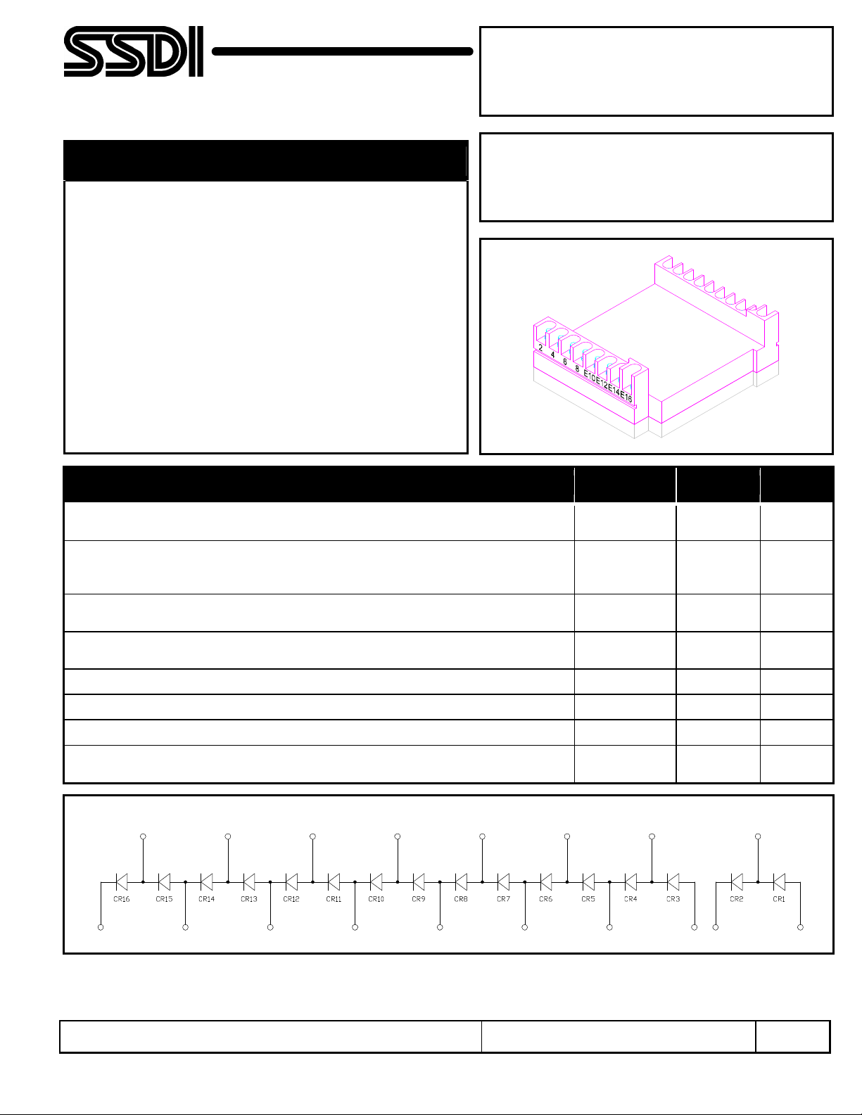
SPA547-01
HYPERFAST HIGH VOLTAGE
DIODE BRIDGE ASSEMBLY
10.5 kV / 1.5A
MAXIMUM RATINGS (Per Leg, Unless Otherwise Specified) Symbol Value Units
Peak Repetitive Reverse Voltage and
DC Blocking Voltage
Half Wave Rectified Forward Current
Averaged Over Fully Cycle
(Resistive Load, 60 Hz, Sine Wave, TC =100oC)
Peak Surge Current
(TC =55oC, 8.3 ms Pulse, Superimposed on Rated Current at Rated Voltage)
Maximum Individual Partial Discharge
(V = 15kV, t = 1min, All Terminals in Common to Base)
Maximum Dielectric Voltage V
Operating Temperature Range (Base plate)
Storage Temperature Range T
Maximum Thermal Resistance (Per Diode)
Junction to Case
Electrical Schematic
E16
E14
E12
E10
E8
E6
V
VR
I
FSM
DIEL
T
OP BASE
R
RRM
IO
STG
θJC
E4
3,000
0.8
40
10
15,000
-45 to +100
-55 to +150
15
Volts
Amps
Amps
pC
Volts
o
o
ºC/W
E2
C
C
19
NOTE: All specifications are subject to change without notification.
SCD’s for these devices should be reviewed by SSDI prior to release.
E17
E15
E13
E11
E9
E7
E5 E3
E1
DATA SHEET #: PM0021D DOC
Page 2
SPA547-01
Solid State Devices, Inc.
14830 Valley View Blvd * La Mirada, Ca 90638
Phone: (562) 404-7855 * Fax: (562) 404-1773
ssdi@ssdi-power.com * www.ssdi-power.com
ELECTRICAL CHARACTERISTICS (Per Leg) Symbol Max Unit
Max Instantaneous Forward Voltage Drop
(IF = 1.0 Adc, TC = 25oC, 300µs Pulse)
Max Reverse Leakage Current
( VR = 3kV, TC = 25oC)
Max Reverse Leakage Current
( VR = 3kV, TC = 100oC)
Maximum Junction Capacitance
(f = 1 MHz, VR =100 V, TC = 25oC)
Maximum Pin to Ground Capacitance
(f = 1 MHz, VR =100 V, TC = 25oC)
Maximum Reverse Recovery Time
(I
= 0.5A, IR = 1.0A, IRR = 0.25A, TC = 25ºC)
F
NOTES:
1. Maximum forward voltage measured with instantaneous forward pulse of 300 µsec minimum.
2. For information on curves, contact the Factory Representative for Engineering Assistance
VF
IR1
IR2
CJ
CB
tRR
8.2
1
50
12
30
40
µA
µA
nsec
V
pF
pF
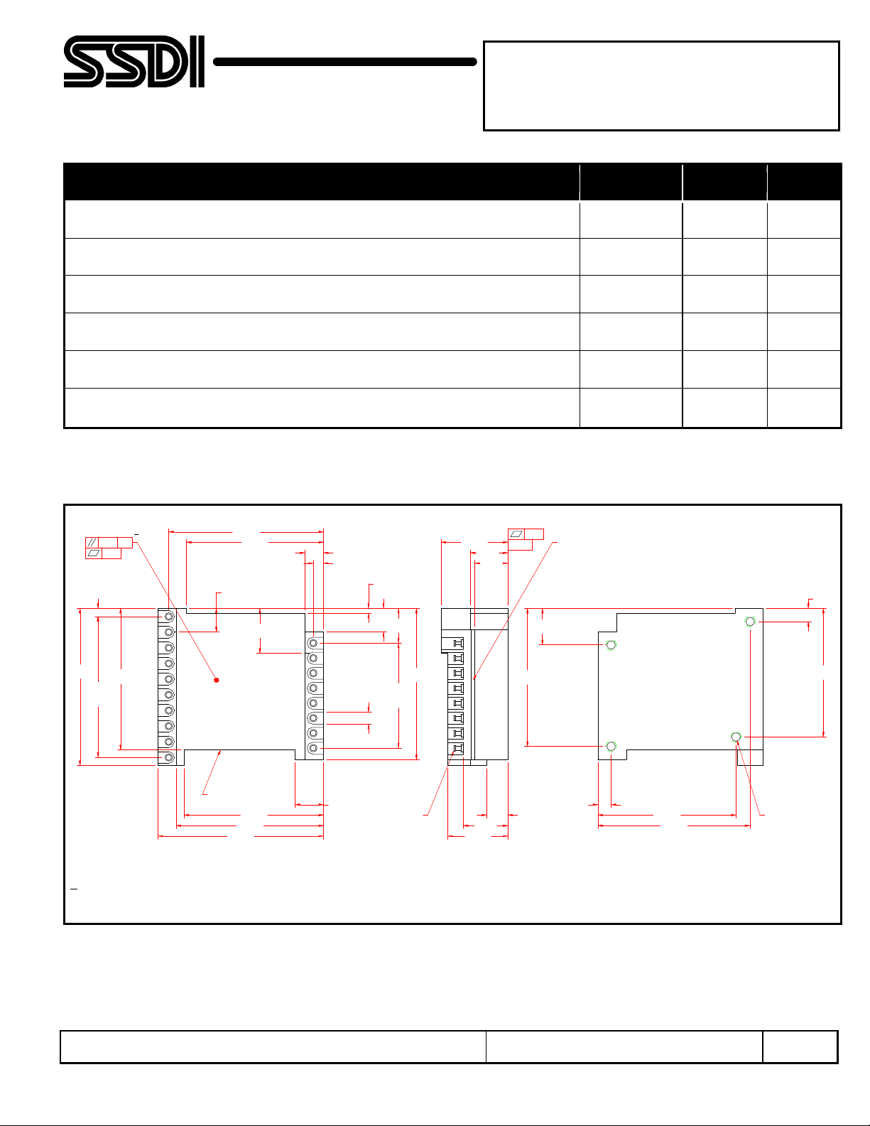
PACKAGE OUTLINE:
2.620
.136
9x .261
(=2.349)
.008 A
.005
2.360
1/
E19
E17
E15
E13
E11
E9
E7
E5
E3
E1
2.579
2.285
.390
.750
MARKING SURFACE
3 PLACES
2.320 .355
2.455
2.755
.310
E16
E14
E12
E10
E8
E6
E4
E2
.470
NOTE:
1/ Specified Flatness and Parallelism applies to
the area of 2.620 x 2.140” min.
.170
18x .200
OR EQUVALENT
.080
.390
.580
2.520
7 x.250
(=1.750)
TERMINAL
160-1512-XX-05
(CAMBION)
1.115
E2 E4 E6 E8 E10 E12 E14 E16
1.000
.630
.745
.550
--A--
2.300
.004
SLOT
.063 WIDE x .040 DEEP
2 SIDES
.610
TOLERANCES:
(UNLESS OTHERWISE SPECIFIED)
.XX ±
.XXX ±
.220
2.300 4x .138-32 UNF-2B
2.535
.02
.010
.220
2.142
HELICOIL INSERT
.315 MIN DEEP
NOTE: All specifications are subject to change without notification.
SCD’s for these devices should be reviewed by SSDI prior to release.
DATA SHEET #: PM0021D DOC
 Loading...